arXiv:1909.13598v2 [physics.app-ph] 4 Dec 2019
Ultrafast sensing of photoconductivity decay using microwave resonators
B. Gy ¨ure-Garami,1B. Blum,1O. S ´agi,1A. Bojtor,1S. Kollarics,1G. Cs ˝osz,1B. G. M ´arkus,1J. Volk,2and F.
Simon1 ,a)
1)Department of Physics, Budapest University of Technology and Economics and MTA- BME Lend¨ulet Spintronics Research Group (PROSPIN), Po. Box 91, H-1521 Budapest, Hungary
2)Institute of Technical Physics and Materials Science, Centre for Energy Research, Konkoly-Thege M. ´ut 29-33, H-1121 Budapest, Hungary
(Dated: 6 December 2019)
Microwave reflectance probed photoconductivity (orµ-PCD) measurement represents a contactless and non-invasive method to characterize impurity content in semiconductors. Major drawbacks of the method include a difficult sep- aration of reflectance due to dielectric and conduction effects and that theµ-PCD signal is prohibitively weak for highly conducting samples. Both of these limitations could be tackled with the use of microwave resonators due to the well-known sensitivity of resonator parameters to minute changes in the material properties combined with a null measurement. A general misconception is that time resolution of resonator measurements is limited beyond their band- width by the readout electronics response time. While it is true for conventional resonator measurements, such as those employing a frequency sweep, we present a time-resolved resonator parameter readout method which overcomes these limitations and allows measurement of complex material parameters and to enhanceµ-PCD signals with the ul- timate time resolution limit being the resonator time constant. This is achieved by detecting the transient response of microwave resonators on the timescale of a few 100 ns duringtheµ-PCD decay signal. The method employs a high-stability oscillator working with a fixed frequency which results in a stable and highly accurate measurement.
I. INTRODUCTION
Microwave detected photoconductivity measurement, µ- PCD1–3, is a standard laboratory and industrial tool to char- acterize the amount of light-excited charge carriers and their lifetime. Knowledge of these parameters is crucial for semiconductor applications in light harvesting and also for the characterization of impurity concentrations. Ex- amples include the characterization of Co and Fe impuri- ties in silicon wafers3,4, the light-induced carrier recombi- nation rate measurements in novel perovskite based photo- voltaic materials5–8, non-silicon semiconductors, e.g. CdSe and CdTe (Ref. 9) and novel low-dimensional materials in- cluding carbon nanotubes10,11, graphene12,13, transition metal dichalcogenides14, and black phosphorus15,16.
The most conventionalµ-PCD implementations rely on de- tecting reflection of microwaves from a sample which is irra- diated using an antenna or an open waveguide, i.e. by non- resonant means. Besides its simplicity, this approach usually suffers from a large, non light-induced reflected background signal that can either saturate the receiver electronics (thus preventing measurement of small light-induced reflections) or perplex the phase sensitive analysis of the back-reflected mi- crowave signal. Measurement of the phase is required in order to separate the reflection due to dielectric and conduction ef- fects. This hindrance is especially pronounced for samples with a high conductivity, i.e. for a doped semiconductor.
It was recognized back in 1977 (Refs. 17 and 18) and re- iterated recently (Ref. 19) that the use of microwave res- onators could eliminate the above mentioned problems since resonators allow for anull measurementand also to improve
a)Corresponding author: f.simon@eik.bme.hu
the sensitivity of the method due to the well-known amplify- ing effect of resonators. The latter can be best demonstrated for considering a single resistor with resistanceRwhose value changes by∆R. In case the resistor is part of a high qual- ity factor (Q) RLC circuit, whose impedance is matched to a waveguide with wave-impedance ofZ0(Z0≫R), the change of the return impedance near the resonance frequency of the resonator is∆Z = ∆R·Z0/R(Ref. 20), i.e. the sensitiv- ity to a small resistance change is significantly enhanced (we present a lumped element circuit model calculation in the Sup- plementary Materials). Equivalently, it is often expressed as
∆R/R= ∆Q/Q(Ref. 21).
The known approach to combine theµ-PCD measurement with microwave resonators involves the detection of power reflected from a resonator during and after a light pulse9,22. However, this method ignores the information contained in the phase (due to the power detection). In addition, both frequency and Q-factor changes lead to a modified reflec- tion, thus modeling to obtain material dependent parameters is rather involved18,23,24. Nevertheless, the approach yields effectiveµ-PCD lifetime values and it was successful in con- structing sensitive electromagnetic radiation detectors21,25–27.
Clearly, a modeling-independent, time-resolved measure- ment of resonator Q and eigenfrequency, f0, is highly de- sired. It is well known that the finite bandwidth of res- onators inherently limits time-resolved measurements to the resonator time constant ofτ = 2Q/ω0, with typical values of τ = 3. . .300ns forQ= 100. . .10,000andf0 = 10GHz.
However, an additional misconception is that the practical measurement of theQ factor and f0 is limited further to a few ms or even seconds, depending on the analyzing elec- tronics in a frequency swept experiment using e.g. a net- work analyzer28–30. This is prohibitively slow for a meaning- ful time-resolved resonator measurement.
We recently reported a novel method31,32 which allows
measurement of the resonator parameters,f0 andQ, with a rapid time domain measurement. The technique shows great resemblance to pulsed nuclear magnetic resonance methods33 and to the optical cavity ring-down spectroscopy34–37. The pulsed resonator readout method employs a short RF pulse with carrier frequency not necessarily matchingf0(fLO6=f0) which induces both a switch-on and switch-off transients.
Both transients represent a decaying oscillation on the eigen- frequency of the resonator,f0(Ref. 38) and with its time con- stant,τ (Refs. 23, 39–41). The transient signals can be con- veniently downconverted with the samefLOfrequency as the exciting signal. Such measurements in the time domain have two important advantages: enhanced accuracy (also known as the Connes advantage42) since the measurement is traced back to a stable frequency, and a simultaneous measurement of the whole resonator response (also known as Fellgett or multiplex advantage43).
This time-resolved, pulsed resonator readout method has been successfully employed to evidence a heating related microwave absorption anomaly in carbon nanotubes44 and to improve the measurement accuracy of power absorbed from an RF field in magnetic ferrite nanoparticles during hyperthermia45. These results motivate the present study to explore the possibility to use this method for the detection of time-resolved µ-PCD studies in silicon. Herein, we re- port time-resolvedµ-PCD measurements for a silicon single crystal samples which are placed inside a microwave cavity resonator with a time constant of about 100 ns. A Q-switch laser induces extra electron-hole pairs in the sample and the laser repetition is synchronized with a train of short mi- crowave pulses. The resulting switch-off transient is detected after each microwave pulse, which yields information about the sample photoconductivity. We present time-resolved res- onatorf0andQdata on a silicon wafer sample withµ-PCD lifetime around 100 µs. The measurement clearly demon- strates the utility of the pulsed resonator readout method for the detection of time-resolved microwave detected photocon- ductivity measurements.
II. PRINCIPLE OF THEµ-PCD MEASUREMENTS A. The conventionalµ-PCD method
In order to illustrate the advances of the present method, we recapture the principle of the conventionalµ-PCD stud- ies. The conventional µ-PCD method is based on detect- ing the reflection of microwaves from a semiconductor wafer.
Reflection of electromagnetic waves from a material can be most conveniently described with the introduction of the wave impedance of the material20,46:
Z=
r iωµ
σ+iωǫ (1)
whereµ = µ0µr is the permeability, ǫ = ǫ0ǫr is the per- mittivity, ω is the angular frequency of the wave, and σ is the conductivity of the sample. In general, µ, ǫ, and σare
complex quantities. Note that Eq. (1) returns the well-known wave impedance of vacuumZ0 = p
µ0/ǫ0 ≈ 377 Ω for µr = ǫr = 1 andσ = 0. For conductors, Z is denoted by the surface impedance, Zs, which highlights that elec- tromagnetic waves penetrate only into the surface of met- als. Then (σ finite, µr = ǫr = 1) and within the quasi- stationary approximation (σ≫ωǫ), the above formula forZ returns the well-known expression for the surface impedance ofZs = q
iωµ0
σ = 1+i2 µ0ωδ, where the penetration depth reads:δ=q
2
µ0ωσ. It also implicitly contains the often used complex dielectric constant for a lossy dielectric (i.e. a di- electric with a finiteσ):eǫr=ǫr−ǫiσ0ω (ǫris the real dielectric constant of the material).
We then consider that the material occupies the half space and it has a surface impedance of Zs. An electromagnetic wave interacts with it, which propagates in free space or in a generic waveguide (it could be a coaxial cable or a TE10 mi- crowave waveguide) thus this medium is modeled with a wave impedance ofZwg. The radiation is reflected from the mate- rial and the reflection coefficient (i.e. ratio of the transmitted to reflected field voltage or amplitude),Γ, is given as20:
Γ = Zs−Zwg
Zs+Zwg
. (2)
In the so-calledS parameter representation,S11 ≈ Γ holds (the equality is strictly valid for zero transmission, see Ref. 46, p. 196). For aµ-PCD experiment in an industrial environ- ment, the reflection is often detected by an antenna, which induces additional geometric factors but it does not affect the generic physical description in Eq. (2).
Eq. (2) is related to the usual Fresnel reflection formula ofr = 11+n−n (for normal incidence of electromagnetic waves from vacuum,n= 1) by recognizing the relation between the wave impedance and the index of refraction as: Z = Z0/en.
The complex index of refraction for a non-magnetic material readsen=√
e ǫr =q
ǫr−ǫiσ0ω.
Alternatively for good conductors, the reflection at low fre- quencies can be approximated with the Hagen-Rubens rela- tion:
R=|r|2= 1−2 r2ǫ0ω
σ . (3)
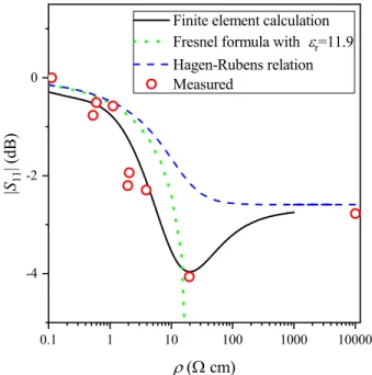
The reflection amplitude, S11, from a silicon single crys- tal wafer with varying resistivity is shown in Fig. 1 for vari- ous approximations: a finite element electromagnetic model- ing for the wafer covering a WR90 X-band waveguide (TE10 mode, 8-12.4 GHz), the Fresnel formula, the Hagen-Rubens relation. We found that the calculated reflections are little af- fected when we considered the small variation ofǫras a func- tion of doping, according to Ref. 47. The figure demonstrates that the Hagen-Rubens relation falls well onto the other two calculations in its domain of validity.
Fig. 1. also contains the experimental results. To obtain these, we covered the WR90 X-band waveguide with a series of silicon single crystal wafers with varying resistivity from
0.1 1 10 100 1000 10000 -4
-2 0
|S11
|(dB)
r (W cm)
Finite element calculation
Fresnel formula with e r
=11.9
Hagen-Rubens relation
Measured
FIG. 1. Reflected microwave amplitude|S11|as a function of the silicon wafer resistivity. Solid curve is a finite element calculation for a WR90 X-band waveguide, covered with the wafers, dashed curve is calculated using the Fresnel formula (as explained in the text), dotted curve is calculation with the Hagen-Rubens relation, and symbols show the experimental data for a set of silicon single crystal wafers.
̺ = 0.528 Ω·cm up to̺ = 10kΩ·cm, i.e. through 4 or- ders of magnitude in̺. We used a copper plate covering the waveguide as|S11| = 0dB reference. As expected, the ex- perimental data lies close to the result of the finite element electromagnetic modeling. The Fresnel formula also demon- strates well the general trend in the reflected amplitude, even if it deviates from the electromagnetic modelling.
In principle, the reflection approach allows to determine the real and imaginary parts of the material parameters from the phase sensitive detection of the reflected microwaves. How- ever, this measurement requires an accurate calibration of the reflected microwave phase. In addition, most µ-PCD mea- surements, which are implemented in an industrial environ- ment, measure the reflected microwave power only. In con- trast, as we shall show below, a measurement of the material parameters in a microwave resonator allows for the automatic disentanglement of the real and imaginary parts of the mate- rial parameters.
Nevertheless, the major hindrance of the conventionalµ- PCD method is that a substantial reflection is present already in dark conditions: as Fig. 1. shows, for most cases the re- flection is around 3 dB, i.e. half of the microwave power is reflected even without illumination. It clearly hinders the de- tection of the extra, light-induced reflection by the saturation of the detecting electronics and the always present dark back- ground gives rise to additional shot noise.
B. The resonator basedµ-PCD method
The so-called cavity perturbation method48,49 is applicable for a sample which is placed inside a microwave cavity res- onator. The presence of the sample affects both the resonance frequency,f0, and quality factor, Q0, of the unloaded res- onator. It was derived in Ref. 50 that the resonator pertur- bation for a cylinder with diameterareads:
∆f f0 −i∆
1 2Q
=−γα (4)
whereγis a sample size dependent constant (also depends on the cavity mode and electromagnetic field distribution). ∆f is the shift in the resonant frequency and∆
1 2Q
is the addi- tional, sample related loss in the cavity. The authors of Ref. 50 introduced theαpolarizability:
α=−2
1− 2 aek
J1
aek J0
aek
(5)
withek = iω√µǫq
1−ωǫ̺i being the complex wavenumber of the microwaves inside the material. J0andJ1are Bessel functions of the first kind.
In the limit of finite electromagnetic wave penetration into the sample, Eq. (4) reduces to the better known expression which relates the resonator parameters directly to the surface impedance according to Eq. (1), as follows20,46,49,51,52
:
∆f f0 −i∆
1 2Q
=−iνZs (6) whereν is a geometry factor (not dimensionless) that is pro- portional to the ratio of the sample surface to the cavity sur- face but it also depends on the resonator mode. We discuss an additional sample geometry and explicitly derive the relation between Eqs. (4) and (6) in the Supplementary Materials.
Eq. (4) shows that measurement of the cavity frequency shift and loss allows to disentangle the real and imaginary parts of the material wave impedance. A limitation of the method is that the geometry factor is generally unknown therefore a calibrating measurement is required to obtain ab- solute material parameter values. The resonator based method prevails when the relative changes in the material parameter is required as a function of time.
Fig. 2. summarizes the change of a microwave resonator parameters for a sample with varying resistivity according to Eq. (4) with theǫr = 11.9for silicon. The behavior can be split to two regimes depending on whether the microwaves penetrate into the sample (penetration limit) or whether it is limited by the skin-effect. For the earlier, the shift is constant and the loss,∆(1/2Q), is linear toσ. In the latter, the skin limit, the real and imaginary parts of Zs are equal and are both proportional to 1/√
σ. This correspondence allows to
0.01 0.1 1 10 100 1000 10000 -2.0
-1.5 -1.0 -0.5 0.0 0.5 1.0 1.5 2.0
Skin Limit Penetration Limit
Shift, Loss µ 1/Ös Shift = const., Loss µ s
Re(a)~-ShiftIm(a)~Loss
r (W cm)
a = 1 mm
a = 10 mm
a = 100 mm e
r = 11.9
FIG. 2. Variation of the resonator parameters according to Eq. (4) with varying silicon resistivity. The two limiting cases are indicated, when microwaves are limited to the skin depth only (skin limit) and when they can penetrate into the sample (penetration limit). Note the characteristically different behavior of the sample parameters in the two regimes versus the sample resistivity.
obtain the material parameters from the measurement of the cavity, besides the ν geometry factor. However, the major advantage of using the microwave resonators is the essentially null measurement it provides.
We emphasize that Eq. (4) gives the cavity perturbation for- mula for an arbitrary value ofσandǫr. Often one discusses the two extremal cases for the cavity perturbation only: e.g. forµ- PCD studies on gas or liquid plasmas17 or on materials with a low conductivity22 the penetration limit is discussed only, whereas the skin-limit with the surface impedance description is used for good conductors53. While the full analysis ofσ andǫr can be performed for the case of cavity perturbation, this is beyond the scope of the present contribution and we focus on the technical development, i.e. on the time-resolved measurement of the resonator shift and loss.
III. THE RESONATOR BASED PHOTOCONDUCTIVITY MEASUREMENT
A. The measurement setup
Our setup for the time-resolved µ-PCD measurement is shown in Fig. 3 including both the conventional (upper panel) and the novel, resonator based approach (lower panel). A Q- switch pulse laser (527 nm Coherent Evolution-15, Nd:YLF) with 1 kHz repetition frequency and∼300ns pulse duration is used for the excitation of charge carriers in the semicon- ductor samples. We note that the 527 nm excitation is capa- ble of photoexciting charge carriers in silicon, even though its
MW source
Pulse laser
Oscilloscope
MW source
Cavity
Pulse laser
Oscilloscope Pin switch
LNA
Si sample LNA Si sample
TTL Generator
L I
R Q L
Q
I R
FIG. 3. Schematics of the conventional (upper panel) and resonator basedµ-PCD decay experiments. A Q-switch laser provides light excitation in both cases. The microwaves are detected with an IQ mixer. In the conventional setup, the signal is measured using re- flectometry, whereas in the novel approach, it is measured through a microwave cavity. A microwave IQ mixer detects the signal in both cases and an optional LNA is indicated with a dashed box. A number of microwave isolators are not shown in the figure.
band edge is around 1100 nm, which would be a more efficient wavelength for such purposes.
The microwave source is a PLL locked synthesizer (HP- Agilent 83751B or a K¨uhne Electronic GmbH model MKU LO 8-13 PLL) which drives the LO of an IQ mixer (Marki Microwave IQ0618LXP double-balanced mixer, LO/RF: 6-18 GHz, IF: DC-500 MHz, 7.5 dB conversion loss). The mixer downconverts the incoming RF signal and the I and Q sig- nals are digitized with an oscilloscope (Tektronix MDO-3024, BW=200 MHz).
Optionally, the RF signal can be amplified by a low noise amplifier (LNA, JaniLab Inc., NF=1.4 dB, Gain=15 dB, 1 dB compression point, P1dB, 10 dBm), which is indicated by a dashed box in the figure. Both the LO and RF inputs of the mixer are isolated galvanically from the rest of the circuit with band-pass (8-12 GHz) DC-blocks. The rising edge of the laser pulses are detected with a fast photodiode (Thorlabs DET36A/M) which provides a jitter-free trigger signal.
This signal triggers the oscilloscope in the conventional setup: therein a standard X-band (8-12.4 GHz) WR90 waveg- uide is used to irradiate samples. The silicon wafers fully cover the waveguide and are illuminated by the light, whose beam aperture is such that it roughly covers the entire waveg- uide opening. We checked that the laser illumination from
the front (i.e. opposite to the microwave irradiation direction) gives qualitatively identical results to those when the sample is irradiated from the back (i.e. parallel to the microwave irra- diation direction). The only difference is that irradiation from the back results in smaller signals as the microwave waveg- uide limits the insertion of light. A standard X-band circula- tor (Ditom Microwave Inc.) acts as duplexing unit between the exciting and reflected microwaves.
In the novel setup, the sample is inside a microwave cav- ity resonator operating in the TE011 mode (with an unloaded quality factor Q0 ≈ 5000) and we use it in transmission.
The cavity is undercoupled for both the input and output (βinput ≈ βoutput ≈ 1/3) which represents a compromise be- tween the resonator bandwidth and transmitted signal20. The parameters of the resonator are measured with the transient method31,32: the exciting microwaves are pulsed, which forces the cavity to transmit microwaves in a transient state. Al- though the exciting carrier frequency, fLO, does not neces- sarily match the resonator eigenfrequency, still the transient signal oscillates on the resonant frequency of the cavity,f0. The carrier of the excitation frequency,fLO, is intentionally detuned fromf0in order to detect the transient with an inter- mediate frequency around5. . .10MHz, which removes the 1/fnoise of the mixer.
The microwave pulses are formed with a fast PIN diode switch (Advanced Technical Materials, S1517D, 5 ns 10-90%
rise-fall transient) which is driven by a TTL signal. This sig- nal contains a switch-on of 0.5µs and is repeated every 2µs.
This duration and repetition are well suited for our cavity with τ≈100ns but these could be further reduced for a cavity with a lowerQ, which would allow for the detection of even faster transients. The optical trigger provides the synchronizing sig- nal for an arbitrary waveform generator (Siglent SDG1025) which generates a train of TTL pulses.
B. Resonator transient measurements
An example for the time-resolved microwave cavity tran- sient method is depicted in Fig. 4. The Q-switch laser pulse (1 ms repetition rate) triggers a train of pulses (each with a duration of 0.5µs followed by another 1.5µs waiting time) which drives the microwave PIN diode. The microwave cav- ity responds with switch-on and off transients. We measure the microwave transients immediately after switching off the microwave excitation as therein the exciting microwave signal is absent. Thus the transient contains information about the resonator only, free from any further signals and can thus be considered as anull measurementof the relevant information.
Two examples for such IQ traces are shown in Fig. 4 for different time delays after the light pulse. These signals are then Fourier transformed to which Lorentzian curves can be fitted. The fitting yields the eigenfrequency and bandwidth of the cavity as a function of the time delay. These directly give the microwave resonator shift and loss, which allows determi- nation of the material parameters according to Eq. 50.
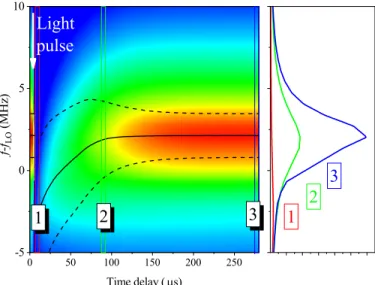
This type of measurement can be also conveniently shown in a three-dimensional contour plot. In Fig. 5., we show the re-
0.0 0.1 0.2 0.3 0.4
-50 0 50
Voltage (mV)
Time delay (ms)
10.90 10.95 11.00 11.05 11.10
-50 0 50
Time delay (s)
Voltage (mV)
I
Q Light pulse
350.90 350.95 351.00 351.05 351.10
50 0 -50
Time delay (s)
FIG. 4. Scheme of the cavity transient detectedµ-PCD. The res- onator transients appear as a train of signals, which contain transients with different frequency and linewidth depending on the state of the sample (Upper panel.). Two examples for such quadrature detected traces (I and Q signals) are shown for different delay times after the light pulse (Lower panel.). These traces are Fourier transformed to yield the microwave cavity resonance curves.
0 50 100 150 200 250
-5 0 5 10
f-fLO
(MHz)
Time delay (ms)
1E-5 9E-5 2.775E-4
a a
3 2
Light
pulse
1 1
2 3
FIG. 5. Time-resolved microwave cavity detectedµ-PCD traces for a silicon sample (̺ = 19.7 Ωcm). The contour plot was obtained by recording consecutive cavity transients after a switch on duration of 0.5µs and a repetition time of 2µs. The contour plot has a loga- rithmic scale to better show the smaller trace values. Solid curve is the shifting of the resonatorf0with respect to the LO frequency and dashed curves indicate the value of the half width of the Lorentzian.
The vertical separation between the two dashed curves is the res- onator bandwidth. The profiles on the right hand side are from the indicated time positions.
sult of the time-resolved resonator readout method for a single crystal silicon wafer sample (̺= 19.7 Ωcm) with a relatively long (about 100µs) charge carrier recombination time. The contour plot also shows the time-dependentf0 −fLO (solid curve) and the half maximum value points of the Lorentzian (dashed curves). The vertical separation between the lat- ter two curves is the resonator bandwidth, BW, which gives Q =f0/BW. A clear time dependence of bothf0 andQis observable from the data. The right hand side of Fig. 5. shows individual Lorentzian resonance profiles which are shown for three different time delays.
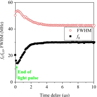
0 2 4 6 8 10
0 20 40 60
FWHM
f 0
f0 -fLO
,FWHM(MHz)
Time delay (ms) End of
light pulse
FIG. 6. Demonstration of the time-resolved microwave cavity de- tectedµ-PCD traces for an ultrafast case. The sample is a silicon wafer (̺ = 0.5 Ωcm). Each individualf0−fLO and FWHM data points were obtained from consecutive cavity transients containing a switch on duration of 50 ns and a repetition time of 200 ns. The latter time resolution,∆tis indicated by an arrow (not to scale). Note that the cavity is strongly loaded with this sample, thusQ≈250.
Fig. 6 shows a time-resolved resonator detected µ-PCD traces for a Si wafer sample which showed an ultrafast charge carrier dynamics less than 2 µs. This was performed on a sample with an already low resistivity,̺ = 0.5 Ωcm, which reduced the cavity quality factor to aboutQ ≈250. This re- sults in a short cavity transient time of aboutτ = 8ns. This allowed to perform the cavity transient experiment with a rep- etition time of 200 ns (time resolution is about the symbol size in the figure), which contained a switch on duration of 50 ns. Clearly, the time-dependent variation of bothf0 and the BW (Q) can be observed from the data. This shows that our method works well for charge carrier life-times down to the microsecond range.
Finally, we highlight several key points of the present de- velopment: our approach does not require frequency stabiliza- tion, or AFC, which was required in alternative studies18,22, except that the irradiating microwave pulse should be within
about 10-100 times the resonator BW with respect to the res- onance frequency. Another important aspect is that we obtain the resonator parameters,f0 andQ, directly from the data, without the need for an involved modeling of the microwave cavity transmission or reflection. Nevertheless, obtaining the time-dependent material parameters (σandǫr) also requires a calculation according to Eq. (4).
The utility of the present method in an industrial environ- ment remains to be addressed. We believe that it may find bet- ter applications in the research of novel semiconductors such as e.g. novel photovoltaic perovskites5–8and low dimensional semiconductor materials including carbon nanotubes10,11, graphene12,13, transition metal dichalcogenides14, and black phosphorus15,16. For such materials sensitivity to material pa- rameters, as well as a sensitive (i.e. background reflection free) measurement of theµ-PCD signal are important rather than the large throughput study of an industrial investigation.
IV. SUMMARY
In summary, we presented an improved approach to de- tect photoinduced conductivity in semiconductors using mi- crowave resonators. Previous studies with microwave res- onators have yielded material parameters after involved mod- eling or with a slow time dynamics (beyond a few ms-second).
Our approach yields directly the resonator parameters, which are in turn related to the material parameters. It is based on the detection of the transient response of a microwave cavity.
While the method encompasses all the known benefits of res- onators in terms of sensitivity and accuracy, its ultimate time resolution is the resonator time constant which can be as low as a few ns.
ACKNOWLEDGEMENTS
The Authors are indebted to Dr. Dario Quintavalle from the Semilab Semiconductor Physics Laboratory Ltd. for useful advises and for providing manufacturing grade silicon wafer samples. This work was supported by the Hungarian Na- tional Research, Development and Innovation Office (NK- FIH) Grant Nrs. 2017-1.2.1-NKP-2017-00001 and K119442, and by the BME-Nanonotechnology FIKP grant of EMMI (BME FIKP-NAT).
1A. Ohsawa, K. Honda, R. Takizawa, and N. Toyokura, Review of Scientific Instruments54, 210 (1983).
2M. Kunst and G. Beck, Journal of Applied Physics60, 3558 (1986).
3K. Lauer, A. Laades, H. Ubensee, H. Metzner, and A. Lawerenz, Journal of Applied Physics104, 104503 (2008).
4B. Berger, N. Schler, S. Anger, B. Grndig-Wendrock, J. R. Niklas, and K. Dornich, physica status solidi (a)208, 769 (2011).
5A. S. Chouhan, N. P. Jasti, S. Hadke, S. Raghavan, and S. Avasthi, Current Applied Physics17, 1335 (2017).
6J. G. Labram and M. L. Chabinyc, Journal of Applied Physics122, 065501 (2017).
7J. A. Guse, A. M. Soufiani, L. Jiang, J. Kim, Y.-B. Cheng, T. W. Schmidt, A. Ho-Baillie, and D. R. McCamey, Phys. Chem. Chem. Phys.18, 12043 (2016).
8Y. Bi, E. M. Hutter, Y. Fang, Q. Dong, J. Huang, and T. J. Savenije, The Journal of Physical Chemistry Letters7, 923 (2016).
9G. Novikov, A. A. Marinin, and E. V. Rabenok, Instruments and Experi- mental Techniques53, 233 (2010).
10M. Freitag, Y. Martin, J. A. Misewich, R. Martel, and P. Avouris, Nano Lett.
3, 1067 (2003).
11S. Lu and B. Panchapakesan, Nanotechnology17, 1843 (2006).
12F. T. Vasko and V. Ryzhii, Phys. Rev. B77, 195433 (2008).
13C. J. Docherty, C.-T. Lin, H. J. Joyce, R. J. Nicholas, L. M. Herz, L.-J. Li, and M. B. Johnston, Nature Communications3, 1228 (2012).
14F. Xia, H. Wang, D. Xiao, M. Dubey, and A. Ramasubramaniam, Nature Photonics8, 899 (2014).
15F. Liu, C. Zhu, L. You, S.-J. Liang, S. Zheng, J. Zhou, Q. Fu, Y. He, Q. Zeng, H. J. Fan, et al., Advanced Materials28, 7768 (2016).
16J. Miao, B. Song, Q. Li, L. Cai, S. Zhang, W. Hu, L. Dong, and C. Wang, ACS Nano11, 6048 (2017).
17P. P. Infelta, M. P. de Haas, and J. M. Warman, Radiation Physics and Chem- istry (1977)10, 353 (1977), ISSN 0146-5724.
18R. W. Fessenden, P. M. Carton, H. Shimamori, and J. C. Scaiano, The Jour- nal of Physical Chemistry86, 3803 (1982).
19O. G. Reid, D. T. Moore, Z. Li, D. Zhao, Y. Yan, K. Zhu, and G. Rumbles, Journal of Physics D: Applied Physics50, 493002 (2017).
20D. M. Pozar,Microwave Engineering(John Wiley & Sons, Inc., 2004).
21B. Cetinoneri, Y. A. Atesal, R. A. Kroeger, G. Tepper, J. Losee, C. Hicks, M. Rasmussen, and G. M. Rebeiz, in2010 IEEE MTT-S International Mi- crowave Symposium(2010), pp. 469–472, ISSN 0149-645X.
22V. Subramanian, V. R. K. Murthy, and J. Sobhanadri, Journal of Applied Physics83, 837 (1998).
23J. Amato, Review of Scientific Instruments53, 776 (1982).
24D. J. Eckstrom, M. S. Williams, and J. Dickinson, Review of Scientific Instruments58, 2244 (1987).
25R. Kessick, G. Tepper, E. Lee, and R. James, Journal of Applied Physics 87, 2408 (2000).
26G. Tepper and J. Losee, Nuclear Instruments and Methods in Physics Re- search Section A: Accelerators, Spectrometers, Detectors and Associated Equipment458, 472 (2001), ISSN 0168-9002, proc. 11th Inbt. Workshop on Room Temperature Semiconductor X- and Gamma-Ray Detectors and Associated Electronics.
27C. Braggio, G. Carugno, A. Lombardi, G. Ruoso, and R. Sirugudu, Journal of Applied Physics116, 044513 (2014).
28P. J. Petersan and S. M. Anlage, Journal of Applied Physics84, 3392 (1998).
29A. Luiten,Q-Factor Measurements(John Wiley & Sons, Inc., 2005), Ency- clopedia of RF and Microwave Engineering.
30D. Kajfez,Q-Factor(John Wiley & Sons, Inc., 2005), Encyclopedia of RF and Microwave Engineering.
31B. Gy¨ure, B. G. M´arkus, B. Bern´ath, F. Mur´anyi, and F. Simon, Review of Scientific Instruments86, 094702 (2015).
32B. Gyre-Garami, O. Sgi, B. G. Mrkus, and F. Simon, Review of Scientific Instruments89, 113903 (2018).
33R. R. Ernst, Angewandte Chemie-International Edition in English31, 805 (1992).
34J. Hodges, H. Layer, W. Miller, and G. Scace, Review of Scientific Instru- ments75, 849 (2004).
35J. Hodges and R. Ciurylo, Review of Scientific Instruments76, 023112 (2005).
36A. Cygan, D. Lisak, P. Maslowski, K. Bielska, S. Wojtewicz, J. Domys- lawska, R. S. Trawinski, R. Ciurylo, H. Abe, and J. T. Hodges, Review of Scientific Instruments82, 063107 (2011).
37G. W. Truong, D. A. Long, A. Cygan, D. Lisak, R. D. van Zee, and J. T.
Hodges, J. Chem. Phys.138, 094201 (2013).
38H. J. Schmitt and H. Zimmer, IEEE Transactions on Microwave Theory and TechniquesMT14, 206 (1966).
39W. Gallagher, IEEE Transactions on Nuclear Science26, 4277 (1979).
40Y. Komachi and S. Tanaka, Journal of Physics E: Scientific Instruments7, 905 (1974).
41R. W. Quine, D. G. Mitchell, and G. R. Eaton, Concepts in Magnetic Reso- nance Part B: Magnetic Resonance Engineering39B, 43 (2011).
42J. Connes and P. Connes, J. Opt. Soc. Am.56(1966).
43P. B. Fellgett,Theory of Infra-Red Sensitivities and its Application to Inves- tigations of Stellar Radiation in the Near Infra-Red (PhD thesis).(Univer- sity of Cambridge, 1949).
44B. G. Mrkus, B. Gyre-Garami, O. Sgi, G. Cssz, A. Karsa, F. Mrkus, and F. Simon, physica status solidi (b)255(2018).
45I. Gresits, G. Thur´oczy, O. S´agi, I. Homolya, G. Bagam´ery, D. Gaj´ari, M. Babos, P. Major, B. G. M´arkus, and F. Simon, Journal of Physics D:
Applied Physics52, 375401 (2019).
46L. Chen, C. Ong, C. Neo, V. Varadan, and V. Varadan,Microwave Elec- tronics: Measurement and Materials Characterization(John Wiley & Sons, Inc., 2004).
47S. Ristic, A. Prijic, and Z. Prijic, Serbian Journal of Electrical Engineering 1, 237 (2004).
48L. I. Buravov and I. F. Shchegolev, Instrum. Exp. Tech.14, 528 (1971).
49O. Klein, S. Donovan, M. Dressel, and G. Gr¨uner, International Journal of Infrared and Millimeter Waves14, 2423 (1993).
50L. D. Landau and E. M. Lifschitz,Electrodynamics of Continuous Media, Course of Theoretical Physics, Vol. 8(Pergamon Press, Oxford, UK, 1984).
51S. Donovan, O. Klein, M. Dressel, K. Holczer, and G. Gr¨uner, International Journal of Infrared and Millimeter Waves14, 2459 (1993).
52M. Dressel, O. Klein, S. Donovan, and G. Gr¨uner, International Journal of Infrared and Millimeter Waves14, 2489 (1993).
53O. Klein, E. J. Nicol, K. Holczer, and G. Gr¨uner, Phys. Rev. B50, 6307 (1994).
54W. R. Thurber, R. L. Mattis, Y. M. Liu, and J. J. Filliben, Journal of The Electrochemical Society127, 2291 (1980).
55W. R. Thurber, R. L. Mattis, Y. M. Liu, and J. J. Filliben, Journal of The Electrochemical Society127, 1807 (1980).
56C. P. Poole,Electron Spin Resonance: A Comprehensive Treatise on Exper- imental Techniques, Dover Books on Physics (Dover Publications, 1996), ISBN 9780486694443.
Appendix A: Physical background of theµ-PCD measurement
In this section, we summarize the most important back- ground knowledge and some supplementary data to the main text.
0 100 200
0 10 20 30 40 50
S AC
(mV)
time delay ( s) 150 mW
500 mW
1000 mW
1500 mW
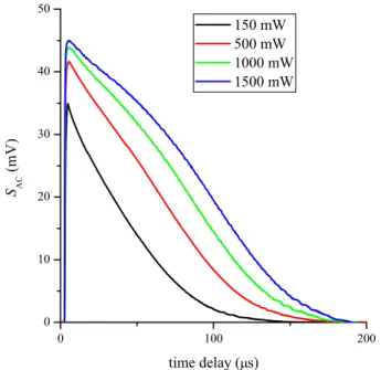
FIG. 7.µ-PCD traces for a silicon single crystal with̺= 19.7 Ωcm resistivity for various irradiation powers (λ = 527nm). Note that 1 W average power corresponds to 1 mJ pulse energy.
In Fig. 7. we show the µ-PCD results for a silicon sin- gle crystal sample which was detected with the conventional method: a silicon wafer covered entirely a WR90 waveguide.
The reflected microwaves were detected from it with and with- out light illumination. In order to calibrate the vertical scale of the µ-PCD traces, it is desired to calibrate the reflected microwave signal voltage by samples with known resistivity.
This would enable to obtain the amount of additional charge carriers from the microwave signal. In the following, we de- note the reflected signal bySDCwithout illumination, and the additional light-induced signal bySAC. We denote the corre- sponding reflection amplitudes, theS11parameter, as ”dark”
and ”illuminated”.
Dashed curve is a purely phenomenological interpolation function (i.e. without any theoretical background) which en- ables to read out the|S11|versus̺correspondence. We used
|S11| = −7.08 + exp
1.78
̺0.134
. Clearly, when illuminated, there is an extra reflection due to the metallicity of the sample.
The extra reflection can be connected to a modified sample resistivity as arrows depict in the figure. This ”illuminated- resisvitity” can be used to determine the amount of light- induced excess charge carrier content from the well-known doping versus resistivity plots54,55.
This enabled us to determine the excess charge carrier con- centration∆nE(t)for each measurement as a function of time.
1 10 100 1000 10000
-6 -4 -2 0
|S 11
|(dB)
( cm) S
11 dark
S 11
illuminated
interpolation
n E
FIG. 8. Dashed curve is a purely empirical stretched exponential fit as explained in the text. Arrows depict how the illuminated reflec- tion amplitude can be used to determine the sample resistivity under illuminated conditions.
The latter information is available from the µ-PCD traces which contain the time-dependent|S11|.
To complete the analysis, we require the charge carrier re- combination time,τc, from theµ-PCD traces, also as a func- tion of time. It is known for the light-induced excess charge carriers that the recombination rate depends on the excess charge carrier concentration itself3. This leads to atime de- pendenceofτc itself. This can be modelled as ∆nE(t) = A×exp
−τct(t)
. We obtain:
τc=
−ln∆nE(t)−lnA t
−1
(A1) In practice, the lnA constant subtraction can be performed, which yields the time-dependentτc.
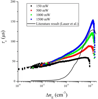
Fig. 9. shows the result of our analysis: namelyτcversus
∆nE is shown for various exciting laser powers. Ideally, all curves with different powers should fall on one another which is not the case in our data. We speculate that this is due to either heating of the sample or due to charge carrier diffu- sion. The latter effect influences the microwave reflectivity as the charge carrier concentration is inhomogeneous along the depth profile of the wafer3. Nevertheless, the trends for all curves agree well with the literature data from Ref. 3, espe- cially around the longestτc.
The excess charge carrier lifetime is limited by various re- laxation rate contributions as follows:
1 τc
= 1 τrad
+ 1 τAuger
+ 1 τSRH
(A2)
10 10
10 12
10 14
10 16 0
50 100 150 200
n E
(cm -3
)
c
(s)
150 mW
500 mW
1000 mW
1500 mW
Literature result (Lauer et al.)
FIG. 9. τcas a function of the excess charge carrier concentration.
Solid curve is a literature data from Ref. 3.
where τrad, τAuger, τSRH are the radiative, Auger, Shock- leyReadHall lifetime contributions, respectively. The radia- tive lifetime, i.e. electron-hole radiative recombination is significant at high electron-hole concentrations. Similarly, the Auger process (the electron-hole recombination energy is taken away by a free charge carrier) becomes significant for high excess charge carrier concentrations. The Shock- leyReadHall process occurs due to impurities which form mid-gap states, e.g. Fe and Cr are known to be typical con- taminant is silicon. The SRH process probability decreases on higher charge carrier concentrations but importantly it domi- natesτ1
c at low excess charge carrier concentration. Thus mea- surement ofτ1
c for low∆nEprovides a direct monitoring mean of the impurity content, which is employed in industrial sili- con wafer characterization.
Fig. 10. shows the contributions from the different excess charge recombination mechanisms and also the resulting to- talτcfor a given Fe impurity content. We also show our data taken at 1500 mW. Note that at the lowest excess charge car- rier concentration, ourτc value tends to 25 µs which is 10 times longer than the example shown herein, indicating an Fe impurity content (provided Fe is the dominant impurity) be- low1012cm−3.
Appendix B: Relation between the generic resonator perturbation and the surface impedance
1. The case of a cylinder
Based on Ref. 50, we gave the generic expression for the resonator perturbation for a cylinder with diameteraas:
10 12
10 14
10 16
10 18 1
10 100 1000 10000
our result Fe: 10
12
cm -3
total
Auger rad
c
(s)
n E
(cm -3
)
FIG. 10. Contribution of the different charge recombination pro- cesses to the excess charge carrier lifetime after Ref. 3. Symbols are the data points from our measurement at 1500 mW average power.
Note the log scale for the charge carrier lifetime.
∆f f0 −i∆
1 2Q
=−γα (B1)
whereγ is a sample size dependent constant (also depends on the cavity mode and electromagnetic field distribution).
∆f is the shift in the resonant frequency and∆
1 2Q
is the change in the resonator bandwidth, BW, (or FWHM) given thatQ=f0/BW thus1/2Q=HWHM/f0, where we intro- duced HWHM (half width at half maximum). The authors of Ref. 50 introduced theαpolarizability:
α=−2
1− 2 aek
J1
aek J0
aek
(B2)
withek = iω√µǫq
1−ωǫ̺i being the complex wavenumber of the microwaves inside the material. J0andJ1are Bessel functions of the first kind.
We then consider the case of finite penetration, i.e. when Im
ek
→ ∞. Then
lim
Im(ek)→∞α= lim
Im(ek)→∞−2
1− 2 aek
J1
aek J0
aek
= (B3)
−2 + 4i
aek ∼const.+iZs. (B4)
The relation between the surface impedance and the wave vec- tor is as follows: Zs = Z0/enandek = ωn/ce (withcbeing the speed of light), which yields: Zs =Z0ω/ekc =Z0/ekλ0, whereλ0 is the wavelength of the electromagnetic wave in vacuum.
We have also used the identity:
ylim→∞
J1(x+iy)
J0(x+iy) =i (B5) Theconst.in Eq. (B4) expresses the fact that the resonator shift is referenced to aperfectconductor (σ = ∞), i.e. one which expels all the electromagnetic fields. This derivation leads us to the well-known formula for the resonator pertur- bation, which contains the surface impedance20,46,49,51,52
:
∆f f0 −i∆
1 2Q
=−iνZs (B6) whereν is a geometry factor (not dimensionless) that is pro- portional to the sample surface to the surface of the cavity but it also depends on the resonator mode.
We also note that the shown Re and Im values of αcan be obtained to match one another when these are shifted by a constant for the case ofσ→ ∞.
2. The case of a sphere
Similarly as before, we can calculate the polarizability of sphere samples from the Helmholtz equation, then we can ob- tain∆f and∆
1 2Q
from Eq. (B1). The polarizability of a sphere sample with diameterais:
α=−3 2
1− 3
a2ek2 + 3 aekcot
aek
, (B7) where the complex wavenumber is the same as before.
In the case of finite penetration:
lim
Im(ek)→∞α= lim
Im(ek)→∞−3 2
1− 3
a2ek2 + 3 aekcot
aek
= (B8)
−3 2 + 9i
2aek ∼const.+iZs, (B9) where we use the identity:
ylim→∞cot (x+iy) =−i. (B10) Note that, the const.terms are different in Eq. (B4) and Eq. (B9) due to the different sample geometry.
Appendix C: The effect of the dielectric constant on the cavity perturbation
In Fig. 11., we show the effect of a finiteǫrfor the resonator shift and loss as calculated for a cylinder with varying diam- eter. Note that in the absence of displacement current related
10 -2
10 -1
10 0
10 1
10 2
10 3
10 4 -2.0
-1.5 -1.0 -0.5 0.0 0.5 1.0 1.5 2.0
Re(a) ~ -Shift Im(a) ~ LossRe(a) ~ -Shift Im(a) ~ Loss
a= 1 mm
a= 10 mm
a= 100 mm e
r = 11.9
10 -2
10 -1
10 0
10 1
10 2
10 3
10 4 -2.0
-1.5 -1.0 -0.5 0.0 0.5 1.0 1.5 2.0
Skin Limit P enetration Limit
Shift, Loss µ 1/Ös Shift=const. , Loss µ s e
r = 0
r (W cm)
FIG. 11. Variation of theαparameter after Ref. 50 for a realistic case of silicon (ǫr = 11.9) and for a good metal, when the dis- placement effects are neglected (ǫr = 0). The lower panel also shows the asymptotic behaviors (dotted curves) for the skin limit:
Loss∝1/√
σ, and for the penetration limit: Loss∝σbehaviors.
effects (σ≫ǫω), both the loss and resonator shift terms have the same magnitude. The figure also shows the asymptotic be- haviors (doted curves) for the skin limit: Loss∝1/√σ, and for the penetration limit: Loss∝σbehaviors. When shifted by 2, the shift value matches exactly the loss for theǫr = 0 case in the skin-limit.
Appendix D: A lumped circuit model calculation of the resonator enhancement effect
We first consider a conventional RLC circuit whose frequency-dependent impedance reads near resonance (ω0 = 1/√
LC):
Z(ω)unmatched≈R+i2RQ0ω−ω0
ω0
, (D1) where the unloaded quality factor readsQ0=Lω0/R.
R C L L
FIG. 12. RLC model of a coupled microwave cavity. Note that the inductorLmodels the matching element.
We then consider an RLC circuit whose impedance is matchedto the wave impedance of the waveguide,Z0. One can model the matching of microwave resonators by the lumped circuit model in Fig. 12 after Refs. 20 and 56. The frequency dependent impedance of such a resonator near the resonance,ω≈ω0reads:
Z(ω)matched≈Z0±i2Z0Qω−ω0
ω0 , (D2) whereQ=Q0/2is the quality factor of a critically coupled resonator.
The minus sign difference stems from the type of match- ing element; the sign is + for a capacitive and - for induc- tive matching (such as that in the figure). Clearly, the differ- ence between Eq. (D2) and Eq. (D1). is that on resonance its impedance istransformedfrom the originalRtoZ0. It is less well known that this transformation property is the principal underlying factor why one uses resonators at all, and how the presence of resonators essentially magnify the sensitivity of material properties measurements.
To demonstrate this, we explicitly express the dependence of the matched resonator parameters on the circuit parameters and then we consider a small perturbation toR. The perturba- tion can be thought of as a small extra absorption in the circuit due to the presence of a sample (or eddy current). It can be shown without the loss of generality that similar conclusion can be drawn when the inductivity in the original circuit is perturbed, e.g. by a piece of a magnetic sample such as that using magnetic resonance.
Ref. 20 derives that for the above circuit the resonance and impedance matching conditions are:
L2ω02=RZ0, (D3) whereω0= 1/p
C(L+L)holds.
Clearly, this equation sets the value ofL. In the highQ limit, Z0 ≫ R, thus L ≪ L, it thus also shows that the resonance frequency is only slightly shifted with respect to ω0= 1/√
LC.
We then consider the sensitivity of the circuit return impedance (orZ(ω)) with respect toR. This is obtained from the change in the corresponding impedances as a function of
a small perturbation inR:R→R+ ∆R. We obtain:
∆ReZunmatched(∆R) = ∂ReZunmatched
∂R ω=ω
0
∆R= ∆R.
(D4) where we used that for an unmatched circuit, such as that de- scribed by Eq. (D1), the following derivative reads:
∂ReZunmatched
∂R
ω=ω0
= 1. (D5)
The sensitivity of the real part impedance of a matched cir- cuit is on the other hand:
∆ReZmatched(∆R) = ∂ReZmatched
∂R
ω=ω0
∆R=±Z0
R∆R.
(D6) where we used that for the impedance of the matched circuit described by Eq. (12) the derivative reads:
∂ReZmatched
∂R ω=ω
0
=±Z0
R. (D7)
We note that the corresponding first order derivatives for the imaginary parts vanish near resonance for both cases. The striking fact about Eqs. (D4) and (D6) is that the matched cir- cuit appears to act as an impedance transformer byZ0/R. We also note that other cases of the resonator perturbation can be similarly considered. E.g. when the resonator is perturbed by a magnetic material, its effect can be taken into account as a change inL, as: L → L(1 +χ), wheree χe = χ′+iχ′′ is the (complex) magnetic susceptibility. Theχ′′ acts as if R was perturbed byLω0χ′′. Thus the above argument applies and the sensitivity for this perturbation reads and its effect is amplified byZ0/R.
The real part,χ′ perturbesLby∆L =Lω0χ′, which has an effect on the imaginary part ofZ(ω). This case:
∆ImZunmatched(∆L) =∂ImZunmatched
∂L ∆L= 2Lω0χ′ω−ω0
ω0
. (D8) For the matched case, we obtain:
∆ImZmatched(∆L) = ∂ImZmatched
∂L ∆L=Z0
R2Lω0χ′ω−ω0
ω0
. (D9) TheZ0/Renhancement factor is often mistaken by an en- hancement effect byQ(orQ0), the reason being that for most resonatorsZ0 ≈ Lω0 holds thusZ0/R ≈ Lω0/R = Q0. TheLω0 ≈Z0can be motivated for a waveguide and a cor- responding resonator: a fundamental mode rectangular res- onator with a mode of TE101, which is made out of a half wavelength section of a TE10 cylindrical waveguide. For both the TE101 cavity and for theλ/2TE10 section, the inductiv- ity isL, and capacitance isC. Given thatZ0 =p
L/C and ω0= 1/√
LC, we get exactlyZ0 =Lω0. Similar arguments hold for other types of resonators such as e.g. aλ/2resonator made of a coplanar waveguide20.
We finally show that one observes a similar up- transformation (i.e. enhancement) effect for the reflection co- efficient. Again, we consider the case of the unmatched and
matched circuits described by Eqs. (D4) and (D6), respec- tively. The reflection coefficients read near resonance (assum- ingZ0≫Rdue to the largeQ):
Γunmatched= R−Z0
R+Z0 ≈1−2R Z0
,Γmatched= Z−Z0
Z+Z0
= 0, (D10) thus the reflection coefficient is close to 1 for the unmatched case which is often disadvantageous, whereas the matched case represents anull measurement.
The corresponding derivatives read:
∂Zunmatched
∂R
ω=ω0
≈ − 2
Z0, ∂Zmatched
∂R
ω=ω0
≈ ± 1 2R.
(D11) Therefore the sensitivity of the reflection coefficient is en- hanced byZ0/4Rfor the case of the matched circuit as com- pared to the unmatched case.
Appendix E: The resonator advantage over a conventional reflection setup
The above discussion is valid for a conventional reflection setup, where the reflected RF voltage is detected with a con- tinuous wave irradiation. As it was shown, the reflectometry method is more sensitive for a matched resonator that for a simple unmatched circuit.
It is also worth discussing the case when the resonator pa- rameters, the frequency shift (∆f) and theQfactor change (∆
1 2Q
), are measured directly. Without the loss of gener- ality, we consider the case of a magnetic sample, whose effect can be well demonstrated. The magnetic sample with a com- plex susceptibility ofχeperturbs a solenoid of an RF circuit as:
L→L(1 +ηχ), wheree ηis the filling factor. Such a sample perturbs the resonator parameters as46,56:
∆f f0 −i∆
1 2Q
=−ηχe (E1)
In the following, we describe the error of theηχemeasure- ment for the non-resonant and resonant cases. In the con- ventional reflectometry technique, it is obtained from the re- flection coefficient,Γ. We consider a waveguide with wave impedanceZ0, which is terminated by an inductor with induc- tanceL. We then introduce the empty reflection coefficient (i.e. without the sample),Γempty, and that with the sample, Γsample. This gives:
ηχe≈iLω+Z0
iLω (Γsample−Γempty), (E2) where we retained leading order terms inηχeonly.
We introduce the standard error of the respective measure- ments asσ(.). Error propagation dictates that
σ(η|χe|)non-resonant= 2σ(Γ)
Γ . (E3)
the||notation is employed asχeis a complex quantity. Our experience with the conventional reflectometry setup using VNAs shows that the quantity on the right hand side is about 10−3..10−4, which fixes the attainable accuracy of the suscep- tibility measurement.
On the other hand, we showed previously31,32that the stan- dard error of∆ff0 can be expressed as:
σ(∆f)
f0 =σ(∆f) BW
BW f0 = 1
Q σ(∆f)
BW . (E4)
where we introduced the resonator bandwidth, BW, which is related to theQasf /BW=Q. We assumed thatf0is error free as it is a dividing constant. We showed in Refs. 31 and 32 that the quantityσ(∆f)BW is typically10−3..10−4. Clearly, a comparison between Eqs. (E3) and (E4) yields that again, the enhancement in the accuracy of the resonator based measure- ment isQ-fold.
The enhancement can be obtained similarly for theQfactor change, by realizing that the error of the shift measurement is the same as the measurement of the BW as it was shown in Refs. 31 and 32.