P´ azmany P´ eter Catholic University
Doctoral Thesis
Parallelization of Numerical Methods on Parallel Processor Architectures
Author:
Endre L´aszl´o
Thesis Advisor:
Dr. P´eter Szolgay, D.Sc.
A thesis submitted in partial fulfillment of the requirements for the degree of Doctor of Philosophy
in the
Roska Tam´as Doctoral School of Sciences and Technology Faculty of Information Technology and Bionics
February 12, 2016
Abstract
Common parallel processor microarchitectures offer a wide variety of solutions to imple- ment numerical algorithms. The efficiency of different algorithms applied to the same problem vary with the underlying architecture which can be a multi-core CPU (Cen- tral Processing Unit), many-core GPU (Graphics Processing Unit), Intel’s MIC (Many Integrated Core) or FPGA (Field Programmable Gate Array) architecture. Significant differences between these architectures exist in the ISA (Instruction Set Architecture) and the way the compute flow is executed. The way parallelism is expressed changes with the ISA, thread management and customization available on the device. These differences pose restrictions for the efficiency of the algorithm to be implemented. The aim of the doctoral work is to analyze the efficiency of the algorithms through the archi- tectural differences and find efficient ways and new efficient algorithms to map problems to the selected parallel processor architectures. The problems selected for the study are numerical algorithms from three problem classes of the 13 Berkeley ”dwarves” [1].
Engineering, scientific and financial applications often require the simultaneous solution of a large number of independent tridiagonal systems of equations with varying coeffi- cients. The dissertation investigates the optimal choice of tridiagonal algorithm for CPU, Intel MIC and NVIDIA GPU with a focus on minimizing the amount of data transfer to and from the main memory using novel algorithms and register blocking mechanism, and maximizing the achieved bandwidth. It also considers block tridiagonal solutions which are sometimes required in CFD (Computational Fluid Dynamic) applications. A novel work-sharing and register blocking based Thomas solver is also presented.
Structured grid problems, like the ADI (Alternating Direction Implicit) method which boils down the solution of PDEs (Partial Differential Equation) into a number of solu- tions of tridiagonal system of equations is shown to improve performance by utilizing new, efficient tridiagonal solvers. Also, solving the one-factor Black-Scholes option pric- ing PDE with explicit and implicit time-marching algorithms on FPGA solution with the Xilinx Vivado HLS (High Level Synthesis) is presented. Performance of the FPGA solver is analyzed and efficiency is discussed. A GPU based implementation of a CNN (Cellular Neural Network) simulator using NVIDIA’s Fermi architecture is presented.
The OP2 project at the University of Oxford aims to help CFD domain scientists to decrease their effort to write efficient, parallel CFD code. In order to increase the effi- ciency of parallel incrementation on unstructured grids OP2 utilizes a mini-partitioning and a two level coloring scheme to identify parallelism during run-time. The use of the GPS (Gibbs-Poole-Stockmeyer) matrix bandwidth minimization algorithm is proposed to help create better mini-partitioning and block coloring by improving the locality of neighboring blocks (also known as mini-paritions) of the original mesh. Exploiting the capabilities of OpenCL for achieving better SIMD (Single Instruction Multiple Data) vectorization on CPU and MIC architectures throught the use of the SIMT (Single Instruction Multiple Thread) programming approach in OP2 is also discussed.
Acknowledgements
I would like to thank my supervisor Prof. Dr. P´eter Szolgay from the P´azm´any P´eter Catholic University for his guidance and valuable support.
I am also grateful to my colleagues Istv´an, Zolt´an, Norbi, Bence, Andr´as, Bal´azs, Antal, Csaba, Vamsi, D´aniel and many others whose discussion helped in the hard problems.
I spent almost two years at the University of Oxford, UK where I met dozens of great minds. First of all, I would like to thank for the supervision of Prof. Dr. Mike Giles who taught me a lot about parallel algorithms, architectures and numerical methods.
I am also grateful to Rahim Lakhoo for the disucssions on technical matters, Eamonn Maguire for his inspiring and motivating thoughts.
All of these would not have been possible without the support of Hajni and my family throughout my PhD studies.
I would like to acknowledge the support of T ´AMOP-4.2.1.B-11/2/KMR-2011-0002 and T ´AMOP-4.2.2/B-10/1-2010-0014 and Campus Hungary. The research at the Oxford e-Research Centre has been partially supported by the ASEArch project on Algorithms and Software for Emerging Architectures, funded by the UK Engineering and Physical Sciences Research Council. Use of the facilities of the University of Oxford Advanced Research Computing (ARC) is also acknowledged.
iii
Contents
Abstract ii
Acknowledgements iii
Contents iv
List of Figures vii
List of Tables xi
Abbreviations xii
Notations and Symbols xv
1 Introduction 1
1.1 Classification of Parallelism . . . 3
1.2 Selected and Parallelized Numerical Problems . . . 7
1.2.1 Tridiagonal System of Equations . . . 7
1.2.2 Alternating Directions Implicit Method . . . 9
1.2.3 Cellular Neural Network . . . 9
1.2.4 Computational Fluid Dynamics . . . 9
1.3 Parallel Processor Architectures . . . 10
1.3.1 GPU: NVIDIA GPU architectures . . . 11
1.3.1.1 The NVIDIA CUDA architecture . . . 11
1.3.1.2 The Fermi hardware architecture. . . 13
1.3.1.3 The Kepler hardware architecture . . . 14
1.3.2 CPU: The Intel Sandy Bridge architecture. . . 15
1.3.3 MIC: The Intel Knights Corner architecture . . . 16
1.3.4 FPGA: The Xilinx Virtex-7 architecture . . . 16
2 Alternating Directions Implicit solver 17 2.1 Introduction. . . 17
2.2 Solving the 3D linear diffusion PDE with ADI. . . 18
3 Scalar Tridiagonal Solvers on Multi and Many Core Architectures 22 3.1 Introduction. . . 22
3.2 Tridiagonal algorithms . . . 23
3.2.1 Thomas algorithm . . . 23 iv
Contents v
3.2.2 Cyclic Reduction . . . 25
3.2.3 Parallel Cyclic Reduction . . . 26
3.2.4 Hybrid Thomas-PCR Algorithm . . . 28
3.3 Data layout in memory . . . 32
3.4 Notable hardware characteristics for tridiagonal solvers. . . 33
3.5 CPU and MIC solution . . . 35
3.6 GPU solution . . . 39
3.6.1 Thomas algorithm with optimized memory access pattern . . . 40
3.6.1.1 Thomas algorithm with local transpose in shared memory 43 3.6.1.2 Thomas algorithm with local transpose using register shuffle . . . 44
3.6.2 Thomas algorithm in higher dimensions . . . 46
3.6.3 Thomas-PCR hybrid algorithm . . . 46
3.7 Performance comparison . . . 47
3.7.1 Scaling in theX dimension . . . 49
3.7.1.1 SIMD solvers . . . 49
3.7.1.2 SIMT solvers . . . 52
3.7.2 Scaling in higher dimensions . . . 54
3.7.2.1 SIMD solvers . . . 54
3.7.2.2 SIMT solvers . . . 55
3.8 Conclusion . . . 56
4 Block Tridiagonal Solvers on Multi and Many Core Architectures 58 4.1 Introduction. . . 58
4.2 Block-Thomas algorithm . . . 59
4.3 Data layout for SIMT architecture . . . 60
4.4 Cooperating threads for increased parallelism on SIMT architecture . . . 62
4.5 Optimization on SIMD architecture. . . 65
4.6 Performance comparison and analysis . . . 66
4.7 Conclusion . . . 70
5 Solving the Black-Scholes PDE with FPGA 71 5.1 Introduction. . . 71
5.2 Black-Scholes equation and its numerical solution . . . 72
5.3 Multi and manycore algorithms . . . 74
5.3.1 Stencil operations for explicit time-marching . . . 74
5.3.2 Thomas algorithm for implicit time-marching . . . 75
5.4 FPGA implementation with Vivado HLS. . . 76
5.4.1 Stencil operations for explicit time-marching . . . 76
5.4.2 Thomas algorithm for implicit time-marching . . . 78
5.5 Performance comparison . . . 78
5.6 Conclusion . . . 79
6 GPU based CNN simulator with double buffering 81 6.1 Introduction. . . 81
6.2 The CNN model . . . 82
6.3 GPU based CNN implementation . . . 84
Contents vi
6.4 CPU based CNN implementation . . . 86
6.5 Comparison of implementations . . . 87
6.6 Conclusion . . . 88
7 Unstructured Grid Computations 89 7.1 Introduction. . . 89
7.2 The OP2 Library . . . 91
7.3 Mini-partitioning and coloring. . . 94
7.3.1 Mesh reordering in Volna OP2 . . . 94
7.3.2 Benchmark . . . 97
7.4 Vectorization with OpenCL . . . 98
7.5 Performance analysis . . . 102
7.5.1 Experimental setup. . . 102
7.5.2 OpenCL performance on CPU and the Xeon Phi . . . 104
7.6 Conclusion . . . 107
8 Conclusion 109 8.1 New scientific results . . . 109
8.2 Application of the results . . . 116
A Appendix 117 A.1 Hardware and Software for Scalar and Block Tridiagonal Solvers . . . 117
A.2 System size configuration for benchmarking block tridiagonal solvers.. . . 119
A.3 Volna OP2 benchmark setup . . . 120
A.4 OpenCL benchmark setup . . . 120
References 121
List of Figures
1.1 Classification of parallelism along with parallel computer and processor architectures that implement them. . . 4 1.2 Roofline model for comparing parallel processor architectures. Note: SP
stands for Single Precision and DP stands for Double Precision. . . 5 1.3 Relations between processor architectures, languages and language exten-
sions.. . . 6 1.4 Roofline model applied to the implemented scalar tridiagonal solvers on
GPU, CPU and MIC processor architectures. The proximity of stars to the upper computational limits shows the optimality of the implementa- tion on the architecture. . . 8 1.5 The increase in computation power. A comparison of NVIDIA GPUs and
Intel CPUs. [20] . . . 11 1.6 The increase in memory bandwidth. A comparison of NVIDIA GPUs and
Intel CPUs. [20] . . . 12 1.7 Kepler and Fermi memory hierarchy according to [22]. The general pur-
pose read-only data cache is known on Fermi architectures as texture cache, as historically it was only used to read textures from global memory. 15 3.1 Starting state of the equation system. 0 values outside the bar are part
of the equation system and they are needed for the algorithm and imple- mentation. . . 31 3.2 State of the equation system after the forward sweep of the modified
Thomas algorithm. . . 31 3.3 State of the equation system after the backward sweep of the modified
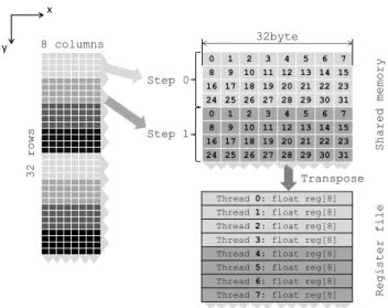
Thomas algorithm. Bold variables show the elements of the reduced sys- tem which is to be solved with the PCR algorithm. . . 31 3.4 Data layout of 3D cube data-structure. . . 32 3.5 Vectorized Thomas solver on CPU and MIC architectures. Data is loaded
into M wide vector registers in M steps. On AVX M = 4 for double precision and M = 8 for single precision. On IMCI M = 8 for double precision andM = 16 for single precision. Data is then transposed within registers as described in Figure 3.6 and after thatM number of iterations of the Thomas algorithm is performed. When this is done the procedure repeats until the and of the systems is reached. . . 38
vii
List of Figures viii 3.6 Local data transposition of anM×M two dimensional array ofM consec-
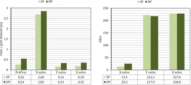
utive values of M systems, where ati is the ith coefficient of tridiagonal system t. Transposition can be performed with M ×log2M AVX or IMCI shuffle type instructions such as swizzle, permute and align or their masked counter part. On AVX M = 4 for double precision and M = 8 for single precision. On IMCI M = 8 for double precision and M = 16 for single precision. . . 38 3.7 ADI kernel execution times on K40m GPU, and corresponding bandwidth
figures for X, Y and Z dimensional solves based on the Thomas algo- rithm. Single precision X dimensional solve is slower×16.75 than theY dimensional solve. Bandwidth is calculated from the amount of data that supposed to loaded and stored and the elapsed time. High bandwidth in the case of Y and Z dimensional solve is reached due to local memory caching and read-only (texture) caching. . . 41 3.8 Local transpose with shared memory. . . 44 3.9 Local transpose with registers. . . 45 3.10 Single precision execution time per grid element. 65536 tridiagonal sys-
tems with varying N X length along the X dimension are solved. CPU, MIC and GPU execution times along with the comparison of the best solver on all three architectures are show. . . 50 3.11 Double precision execution time per grid element. 65536 tridiagonal sys-
tems with varying N X length along the X dimension are solved. CPU, MIC and GPU execution times along with the comparison of the best solver on all three architectures are show. . . 51 3.12 Single and double precision execution time per grid element. 65536 tridi-
agonal systems with varyingN Y length along the Y dimension are solved.
CPU, MIC and GPU execution times along with the comparison of the best solver on all three architectures are show. . . 55 3.13 Grid element execution times per grid element on a 240×256×256 cube
domain. X dimension is chosen to be 240 to alleviate the effect of caching and algorithmic inefficiencies which occurs on sizes of power of 2 as it can be seen on Figures 3.10,3.11,3.12. Missing bars and n/a values are due to non-feasible or non-advantagous implementations in the Y dimension. . . 57 4.1 Data layout within coefficient array A. This layout allows nearly coa-
lesced access pattern and high cache hit rate when coalescence criteria is not met. Here Apn is the nth block (ie. nth block-row in the coefficient matrix) of problem pand p∈[0, P −1], n∈[0, N −1]. Notation for the scalar elements in the nth block of problem p are shown on Eq. (4.3).
Bottom part of the figure shows the mapping of scalar values to the linear main memory. . . 61 4.2 Data layout of d as block vectors. This layout allows nearly coalesced
access pattern and high cache hit rate when coalescence criteria is not met. Heredpnis thenth block (ie. nth block-row in the coefficient matrix) of problem p and p ∈ [0, P −1], n∈ [0, N −1]. Notation for the scalar elements in the nth block of problem p are shown on Eq. (4.4). Bottom part of the figure shows the mapping of scalar values to the linear main memory. . . 61
List of Figures ix 4.3 Shared storage of blocks in registers. Arrows show load order. Thread
T0,T1 andT2 stores the first, second and third columns of blockApn and first, second and third values ofdpn.. . . 63 4.4 Data layout within coefficient array A suited for better data locality on
CPU and MIC. HereApnis thenth block (ie. nth block-row in the coeffi- cient matrix) of problem pandp∈[0, P−1],n∈[0, N−1]. Notation for the scalar elements in the nth block of problemp are shown on Eq. (4.3). 65 4.5 Single (left) and double (right) precision effective bandwidth when solv-
ing block tridiagonal systems with varying M block sizes. Bandwidth is computed based on the amount of data to be transfered. Caching in L1 and registers can make this figure higher then the achievable bandwidth with a bandwidth test. . . 67 4.6 Single (left) and double (right) precision effective computational through-
put when solving block tridiagonal systems with varying M block sizes.
GFLOPS is computed based on the amount of floating point arithmetic operations needed to accomplish the task. Addition, multiplication and division is considered as floating point arithmetic operations, ie. FMA (Fused Multiply and Add) is considered as two floating point instructions. 68 4.7 Single (left) and double (right) precision block-tridiagonal solver execu-
tion time per block matrix row for varying block sizes. . . 69 4.8 Single (left) and double (right) precision block tridiagonal solver speedup
over the CPU MKL banded solver. . . 69 5.1 Stacked FPGA processing elements to pipeline stencil operations in a sys-
tolic fashion. The initial system variables u(0)0 , ..., u(0)K−1 are swept by the first processing element. The resultu(1)k+1is fed into the second processing element. . . 77 6.1 Left: standard CNN (Cellular Neural Network) architecture. Right: CNN
local connectivity to neighbor cells. Source: [64]. . . 82 6.2 Piecewise linear output function defined in Eq. (6.2). Source: [64] . . . . 83 6.3 Example of diffuson template. Original image on the left, diffused image
on the right.. . . 84 6.4 The use of texture and constant caching - code snippets from source code. 85 7.1 Demonstrative example of the OP2 API in Airfoil: parallel execution of
theres calckernel function by theop par loopfor each elements in the edges set. . . 92 7.2 Demonstrative example of block coloring: edges are partitioned into three
blocks colors. Indices of edges belonging to different colors are shuffled in the linear memory. . . 93 7.3 Example of sparse symmetric matrix or adjacency matrix representing an
unstructured mesh (left) and the same matrix after matrix bandwidth minimization reordering (right). Elements connecting the vertices of the first block (elements 0-19) of the mesh with other blocks of the mesh (20- 39, 40-59, etc.) are denoted with red color. On the left matrix the first block of the mesh is connected to other blocks. On the right matrix the first block is only connected to the second block. . . 95 7.4 Demonstrative examples of the Volna OP2 test cases. . . 95
List of Figures x 7.5 Reordering the mesh and associated data of Volna OP2 based on GPS
reordering. Mesh component such as the cells, edges and nodes as well as their associated data are separately reorder. op get permutation in- ternally creates an adjacency matrix of cells based on the cells-to-cells, cells-to-edges or cells-to-nodes connectivity. . . 96 7.6 The effect of mesh reordering on the block colors and execution time.. . . 98 7.7 Simplified example of code generated for the OpenCL vectorized backend. 100 7.8 Pseudo-code for OpenCL work distribution and vectorization. . . 101 7.9 Vectorization with OpenCL compared to previous implementations. Perfor-
mance results from Airfoil in single (SP) and double (DP) precision on the 2.8M cell mesh and from Volna in single precision on CPU. . . . 106 7.10 Performance of OpenCL compared to non-vectorized, auto-vectorized and ex-
plicitly vectorized (using intrinsic instructions) versions on the Xeon Phi using Airfoil (2.8M cell mesh) and Volna test cases. . . . 107 8.1 Thesis groups: relation between thesis groups, parallel problem classifi-
cation and parallel processor architectures. Colored vertical bars right to thesis number denote the processor architecture that is used in that thesis. Dashed grey arrow represent relation between theses.. . . 110
List of Tables
2.1 Number of parallel systems increases rapidly as dimensiondis increased.
N is chosen to accommodate an Nd single precision problem domain on
the available 12 GB of an NVIDIA Tesla K40 GPU. . . 18
5.1 FPGA Resource statistics for a single processor. The final number of implementable explicit solvers is bounded by the 3600 DSP slices, while the number of implicit solvers is bounded by the 2940 Block RAM Blocks on the Xilinx Virtex-7 XC7V690T processor. . . 78
5.2 Performance - Single Precision . . . 79
5.3 Performance - Double Precision . . . 79
6.1 Comparison table . . . 87
7.1 Details of the representative tsunami test cases. BW - Bandwidth . . . . 97
7.2 Properties of Airfoil and Volna kernels; number of floating point opera- tions and numbers transfers . . . 103
7.3 Test mesh sizes and memory footprint in double(single) precision . . . 104
7.4 Useful bandwidth (BW - GB/s) and computational (Comp - GFLOP/s) throughput baseline implementations on Airfoil (double precision) and Volna (single precision) on CPU 1 and the K40 GPU . . . 105
7.5 Timing and bandwidth breakdowns for the Airfoil benchmarks in dou- ble(single) precision on the 2.8M cell mesh and Volna using the OpenCL backend on a single socket of CPU and Xeon Phi. Also, kernels with implicit OpenCL vectorization are marked in the right columns.. . . 106
A.1 Details of Intel Xeon Sandy Bridge server processor, Intel Xeon Phi co- processor and the NVIDIA Tesla GPU card. *Estimates are based on [23], [44] and [94]. Both Intel architectures have 8-way, shared LLC with ring-bus topology. HT - Hyper Thread, MM - Multi Media, RO - Read Only . . . 118
A.2 Parameter N - Length of a system used for benchmarking a processor architecture and solver. The length of the system is chosen such that the problem fits into the memory of the selected architecture. . . 119
A.3 Parameter P - Number of systems used for benchmarking a processor architecture and solver. The number of systems is chosen such that the problem fits into the memory of the selected architecture. . . 119
A.4 Details of Intel Xeon Haswell server processor used in the benchmarks of Volna OP2. HT - Hyper Thread, MM - Multi Media . . . 120
A.5 Benchmark systems specifications . . . 120
xi
Abbreviations
ADI Alternating Directions Implicit method ALU Arithmetic Logic Unit
AoS Array of Structures
ARM AdvancedRISCMachine Holdings Plc.
ASIC ApplicationSpecificIntegratedCircuit
ASM Asembly
AVX AdvancedVector Extensions BRAM BlockRAM
BS Black-Scholes
CFD Computational Fluid Dynamics CLB Configurable Logic Block
CMOS Complementary Metal-Oxide-Semiconductor CNN CellularNeuralNetwork
CPU Central Processing Unit CR Cyclic Reduction
CUDA ComputeUnifiedDeviceArchitecture DDR Double DataRate
DP Double Precision
DSL DomainSpecificLanguage DSP Digital SignalProcessing FLOP Floating PointOPeration
FLOPS Floating PointOerations PerSecond FMA Fused Multiply andAdd
FPGA Field ProgrammableGateArray GPS Gibbs-Poole-Stockmeyer
xii
Abbreviations xiii
GPGPU General Purpose GPU GPU Graphics Processing Unit HDL Hardware Description Language HLS High Level Synthesis
HPC High Performance Computing HT Hyper Threading
HTT Hyper ThreadingTechnology IC IntegratedCircuit
IEEE Institute of Electrical and Electronics Engineers IMCI InitialMany CoreInstructions
IPP (Intel)IntegratedPerformancePrimitives ISA InstructionSet Architecture
KNC KNights Landing L1/2/3 Level 1/2/3
LAPACK LinearAlgebraPackage LHS LeftHand Side
LLC LastLevelCache MAD Multiply And Add MIC Many IntegratedCore MKL Math KernelLibrary MLP MultiLayerPerceptron MOS Metal-Oxide-Semiconductor MPI Message PassingInterface MSE MeanSquareError
NNZ Number of Non-Zero elements NUMA Non-UniformMemory Access NVVP NVIDIAVisual Profiler NZ Non-Zero element
ODE Ordinary Differential Equations OpenACC Open Accelerators
OpenCL Open Computing Language OpenMP Open Multi-Processing PCR Parallel Cyclic Reduction
Abbreviations xiv
PDE Partial DifferentialEquations PTX Parallel Thread Exexcution RAM RandomAccessMemory RHS RightHandSide
ScaLAPACK ScalableLinearAlgebraPackage SDRAM Synchronous Dynamic RAM SIMD SingleInstruction Multiple Data SIMT SingleInstruction Multiple Thread SMP SimultaneousMultiProcessing SMT SimultaneousMultiThreading SMX StreamingMultiprocessor - eXtended SoA Structuresof Array
SP SinglePrecision
SPARC Scalable Processor Architecture International, Inc.
TLB TranslationLookaside Buffer TDP ThermalDesignPower UMA UniformMemory Access
VHDL VHSIC HardwareDescriptionLanguage VHSIC Very HighSpeedIntegrated Circuit VLIW Very Long InstructionWord
VLSI Very Large Scale Integration WAR WriteAfterRead
Notations and Symbols
R Set of real numbers
R+ Set of non-negative real numbers
V Volt
W Watt
GB Giga bytes, 210 bytes; used instead of IEC GiB standard
GB/s Giga bytes per second, 210 bytes per second; used instead of IEC GiB/s standard
xv
Chapter 1
Introduction
Limits of physics Today the development of every scientific, engineering and finan- cial field that rely on computational methods is severely limited by the stagnation of computational performance caused by the physical limits in the VLSI (Very Large Scale Integration) technology. This is caused by the single processor performance of the CPU (Central Processing Unit) due to vast heat dissipation that can not be increased. Around 2004 this physical limit made it necessary to apply more processors onto a silicon die and so the problem of efficient parallelization of numerical methods and algorithms on a processor with multiple cores was born.
The primary aim of my thesis work is to take advantage of the computational power of various modern parallel processor architectures to accelerate the computational speed of some of the scientific, engineering and financial problems by giving new algorithms and solutions.
After the introduction of the problems and limits behind this paradigm shift in the current section, a more detailed explanation of the classification and complexity of par- allelization is presented in Section 1.1. Section 1.2 introduces the numerical problems on which the new scientific results of Section8.1 rely.
Gordon Moore in the 1960’s studied the development of the CMOS (Complementary Metal-Oxide-Semiconductor) manufacturing process of integrated circuits (IC). In 1965 he concluded from five manufactured ICs, that the number of transistors on a given silicon area will double every year. This finding is still valid after half a century with
1
Chapter 1. Introduction 2 a major modification: the number of transistors on a chip doubles every two years (as opposed to the original year).
This law is especially interesting since around 2004 the manufacturing process reached a technological limit, which prevents us from increasing the clock rate of the digital circuitry. This limit is due to the heat dissipation. The amount of heat dissipated on the surface of a silicon die of size of a few square centimetres is in the order 100s of Watts. This is the absolute upper limit of the TDP (Thermal Design Power) that a processor can have. The ever shrinking VLSI feature sizes cause: 1) the resistance (and impedance) of conductors to increase; 2) the parasitic capacitance to increase; 3) leakage current on insulators like the MOS transistor gate oxide to increase. These increasing resistance and capacitance related parameters limit the clock rate of the circuitry. In order to increase the clock rate with these parameters the current needs to be increased and that leads to increased power dissipation. Besides limiting the clock rate the data transfer rate is also limited by the same physical facts.
The TDP of a digital circuit is composed in the following way: PT DP =PDY N +PSC+ PLEAK, where PDY N is the dynamic switching, PSC is the instantaneous short circuit (due to non-zero rise or fall times) and PLEAK is the leakage current induced power dissipation. The most dominant power dissipation is due to the dynamic switching PDY N ∝CV2f, where ∝indicates proportionality, f is the clock rate, C is the capaci- tance arising in the circuitry and V is the voltage applied to the capacitances.
Temporary solution to avoid the limits of physics – Parallelisation Earlier, the continuous development of computer engineering meant increasing the clock rate and the number of transistors on a silicon die, as it directly increased the computational power. Today, the strict focus is on increasing the computational capacity with new solutions rather than increasing the clock rate on the chip. One solution is to parallelise on all levels of a processor architecture with the cost of cramming more processors and transistors on a single die. The parallelisation and specialization of hardware necessarily increases the hardware, algorithmic and software complexity. Therefore, since 2004 new processor architectures appeared with multiple processor cores on a single silicon die.
Also, more and more emphasise is put to increase the parallelism on the lowest levels of the architecture. As there are many levels of parallelism built into the systems today,
Chapter 1. Introduction 3 the classification of these levels is important to understand what algorithmic features can be exploited during the development of an algorithm.
Amdahl’s law Gene Amdahl at a conference in 1967 [2] gave a talk on the achievable scaling of single processor performance to multiple processors assuming a fixed amount of work to be performed. Later, this has been formulated as Eq. (1.1) and now it is know as Amdahl’s law. Amdahl’s law states that the speedup due to putting the P part of the workload of a single processor onto N identical processors results in S(N) speedup compared to single processor.
S(N) = 1
(1−P) +NP (1.1)
One may think of the proportion P as the workload that has been parallelized by an algorithm (and implementation). The larger this proportion, the better the scaling of the implementation will be. This setup is also known as strong scaling. This is a highly important concept that is implicitly used in the arguments when parallelization is discussed.
Gustafson’s law John Gustafson in 1988 reevaluated Amdahl’s law [3] and stated that in the framework of weak scaling the speedup is given by Eq. (1.2). Weak scaling measures the execution time when the problem size is increasedN fold when the prob- lem is scheduled onto N parallel processors. Eq. (1.2) states that the execution time (Slatency(s)) decreases when the latency due to the P proportion - which benefits from the parallelization - speeds up by a factor of s.
Slatency(s) = 1−P +sP (1.2)
1.1 Classification of Parallelism
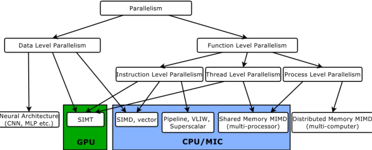
The graph presented on Figure 1.1. shows the logical classification of parallelism on all levels. Leaves of the graph show the processor features and software components that implement the parallelism. Processor and software features highlighted as GPU
Chapter 1. Introduction 4 (Graphics Processing Unit) and CPU/MIC (MIC - Many Integrated Core) features are key components used in the work.
Parallelism
Data Level Parallelism Function Level Parallelism
Neural Architecture
(CNN, MLP etc.) SIMD, vector
Instruction Level Parallelism Thread Level Parallelism Process Level Parallelism
Distributed Memory MIMD (multi-computer) Shared Memory MIMD
(multi-processor)
SIMT Pipeline, VLIW,
Superscalar
GPU CPU/MIC
Figure 1.1: Classification of parallelism along with parallel computer and processor architec- tures that implement them.
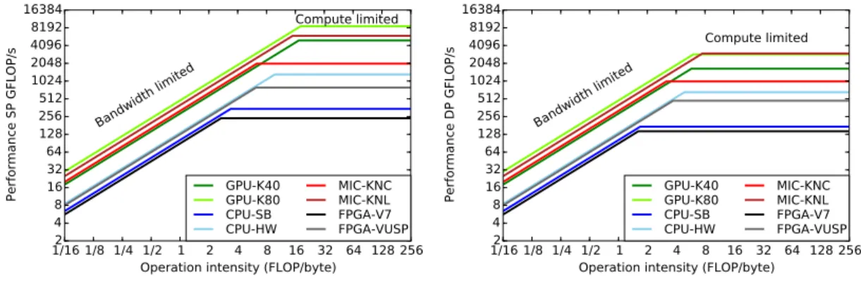
Architecture dependent performance bounds Depending on the design aims of a parallel processor architecture the computational performance of these architectures vary with the problem. The performance can be bound by the lack of some resources needed for that particular problem, eg. more floating point units, greater memory bandwidth etc. Therefore it is common to refer to an implementation being: 1)compute bound if further performance gain would only be possible with more compute capability or 2) memory bandwidth bound if the problem would gain performance from higher memory bandwidth. The roofline model [4] helps identifying whether the computational performance of the processor on a given algorithm or implementation is bounded by the available computational or memory controller resources and also helps approximating the extent of the utilization of a certain architecture. See Figure 1.2 for comparing parallel processor architectures used in the dissertation. Processor architectures that were recently introduced to the marker and which are to be announced are also noted on the figure.
On Figure1.2the graphs were constructed based on the maximum theoretical computa- tional capacity (GFLOP/s) and data bandwidth (GB/s) metrics. In the case of FPGAs the number of implementable multipliers and the number of implementable memory interfaces working at the maximum clock rate gives the base for the calculation of the graphs. The exact processor architectures behind the labels are the following: 1) GPU- K40: NVIDIA Tesla K40m card with Kepler GK110B microarchitecture working with
Chapter 1. Introduction 5
“Boost” clock rate; 2) GPU-K80: NVIDIA Tesla K80 card with Kepler GK210 microar- chitecture working with “Boost” clock rate; 3) CPU-SB: Intel Xeon E5-2680 CPU with Sandy Bridge microarchitecture; 4) CPU-HW: Intel Xeon E5-2699v3 CPU with Haswell microarchitecture; 5) MIC-KNC: Intel Xeon Phi 5110P co-processor card with Knights Corner microarchitecture; 6) MIC-KNL: Intel Xeon Phi co-processor with Knights Land- ing microarchitecture - the exact product signature is yet to be announced; 7) FPGA-V7:
Xilinx Virtex-7 XC7VX690T; 8) FPGA-VUSP: Xilinx Virtex UltraScale+ VU13P.
As the aim of my work was achieving the fastest execution time by parallelization the roofline model is used to study the computational performance of the selected problems where applicable.
1/16 1/8 1/4 1/2 1 2 4 8 16 32 64 128 256 Operation intensity (FLOP/byte)
24 168 6432 128256 1024512 204840968192 16384
Performance SP GFLOP/s
Bandwidth limited
Compute limited
GPU-K40 GPU-K80 CPU-SB CPU-HW
MIC-KNC MIC-KNL FPGA-V7 FPGA-VUSP
1/16 1/8 1/4 1/2 1 2 4 8 16 32 64 128 256 Operation intensity (FLOP/byte)
42 168 3264 128256 1024512 409620488192 16384
Performance DP GFLOP/s
Bandwidth limited
Compute limited
GPU-K40 GPU-K80 CPU-SB CPU-HW
MIC-KNC MIC-KNL FPGA-V7 FPGA-VUSP
Figure 1.2: Roofline model for comparing parallel processor architectures. Note: SP stands for Single Precision and DP stands for Double Precision.
Parallel Processor Architectures and Languages A vast variety of parallel archi- tectures are used and experimented in HPC (High Performance Computing) to compute scientific problems. Multi-core Xeon class server CPU by Intel is the leading architecture used nowadays in HPC. GPUs (Graphics Processing Unit) originally used for graphics- only computing has become a widely used architecture to solve certain problems. In recent years Intel introduced the MIC (Many Integrated Core) architecture in the Xeon Phi coprocessor family. IBM with the POWER and Fujitsu with the SPARC processor families are focusing on HPC. FPGAs (Field Programmable Gate Array) by Xilinx and Altera are also used for the solution of some special problems. ARM as an IP (Intellec- tual Property) provider is also making new designs for x86 CPU processors which find application in certain areas of HPC. Also, research is conducted to create new heteroge- nous computing architectures to solve the power efficiency and programmability issues of CPUs and accelerators.
Chapter 1. Introduction 6 Programming languages like FORTRAN, C/C++ or Python are no longer enough to exploit the parallelism of these multi- and many-core architectures in a productive way.
Therefore, new languages, language extensions, libraries, frameworks and DSLs (Domain Specific Language) appeared in recent years, see Figure 1.3. Without completeness the most important of these are: 1) CUDA (Compute Unified Device Architecture) C for programming NVIDIA GPUs; 2) OpenMP (Open Multi Processing) directive based lan- guages extension for programming multi-core CPU or many-core MIC architectures; 3) OpenCL (Open Compute Language) for code portable, highly parallel abstraction; 4) AVX (Advanced Vector eXtension) and IMCI (Initial Many Core Instruction) vector- ized, SIMD (Single Instruction Multiple Data) ISA (Instruction Set Architecture) and intrinsic instructions for increased ILP (Instruction Level Parallelism) in CPU and MIC;
5) OpenACC (Open Accelerators) directive based language extension for accelerator ar- chitectures; 6) HLS (High Level Synthesis) by Xilinx for improved code productivity on FPGAs.
All these new architectural and programming features raise new ways to solve existing parallelisation problems, but non of them provide high development productivity, code- and performance portability as one solution. Therefore, these problems are the topic of many ongoing research in the HPC community.
CPU x86 Intel MIC NVIDIA GPU AMD GPU FPGA
MPI OpenMP intrinsicASM OpenCL OpenACC CUDA VerilogVHDL HLS
Figure 1.3: Relations between processor architectures, languages and language extensions.
Classification of problem classes according to parallelization Classification of the selected problems is based on the 13 “dwarves” of “A view of the parallel computing landscape” [1]. My results are related to the dwarves highlighted with bold fonts:
1. Dense Linear Algebra 2. Sparse Linear Algebra 3. Spectral Methods
4. N-Body Methods 5. Structured Grids
6. Unstructured Grids 7. MapReduce
8. Combinational Logic 9. Graph Traversal 10. Dynamic Programming
Chapter 1. Introduction 7 11. Backtrack and Branch-and-Bound
12. Graphical Models
13. Finite State Machines
1.2 Selected and Parallelized Numerical Problems
The selected numerical algorithms cover the fields of numerical mathematics that aim for the solution of PDEs (Partial Differential Equation) in different engineering ap- plication areas, such as CFD (Computational Fluid Dynamics), financial engineering, electromagnetic simulation or image processing.
1.2.1 Tridiagonal System of Equations
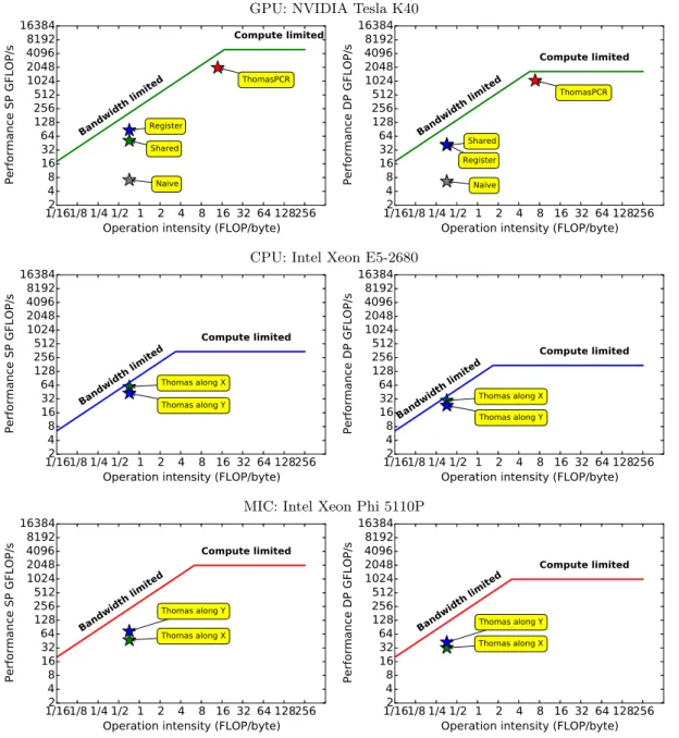
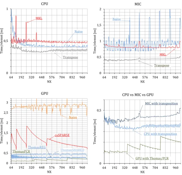
Engineering, scientific and financial applications often require the simultaneous solution of a large number of independent tridiagonal systems of equations with varying coef- ficients [5, 6, 7, 8, 9, 10]. The solution of tridiagonal systems also arises when using line-implicit smoothers as part of a multi-grid solver [11], and when using high-order compact differencing [12, 13]. Since the number of systems is large enough to offer considerable parallelism on many-core systems, the choice between different tridiagonal solution algorithms, such as Thomas, CR (Cyclic Reduction) or PCR (Parallel Cyclic Reduction) needs to be re-examined. In my work I developed and implemented near optimal scalar and block tridiagonal algorithms for CPU, Intel MIC and NVIDIA GPU with a focus on minimizing the amount of data transfer to and from the main memory using novel algorithms and register blocking mechanism, and maximizing the achieved bandwidth. The latter means that the achieved computational performance is also max- imized (see Figure 1.4) as the solution of tridiagonal system of equations is bandwidth limited due to the operation intensity.
On Figure 1.4 the computational upper limits on the graphs were constructed based on the maximum theoretical computational capacity (GFLOP/s) and data bandwidth (GB/s) metrics of the three processors. The operation intensity is calculated from the amount of data that is moved through the memory bus and the amount of floating point operations performed on this data. The total amount of floating point operations is calculated and divided by the execution time to get the performance in GFLOP/s. The
Chapter 1. Introduction 8 operation intensity and GFLOP/s performance metrics are calculated for each solver and they are represented with stars on the figures.
In most cases the tridiagonal systems are scalar, with one unknown per grid point, but this is not always the case. For example, computational fluid dynamics applications often have systems with block-tridiagonal structure up to 8 unknowns per grid point [7]. The solution of block tridiagonal system of equations are also considered which are sometimes required in CFD (Computational Fluid Dynamic) applications. A novel work-sharing and register blocking based Thomas solver for GPUs is also created.
GPU: NVIDIA Tesla K40
1/161/8 1/4 1/2 1 2 4 8 16 32 64 128256 Operation intensity (FLOP/byte) 428
1632 12864 256512 10242048 40968192 16384
Performance SP GFLOP/s Naive
Shared Register
ThomasPCR
Bandwidth limited
Compute limited
1/161/8 1/4 1/2 1 2 4 8 16 32 64 128256 Operation intensity (FLOP/byte) 428
1632 12864 256512 10242048 40968192 16384
Performance DP GFLOP/s Naive
Shared Register
ThomasPCR
Bandwidth limited
Compute limited
CPU: Intel Xeon E5-2680
1/161/8 1/4 1/2 1 2 4 8 16 32 64 128256 Operation intensity (FLOP/byte) 428
1632 12864 256512 10242048 40968192 16384
Performance SP GFLOP/s
Thomas along X Thomas along Y
Bandwidth limited
Compute limited
1/161/8 1/4 1/2 1 2 4 8 16 32 64 128256 Operation intensity (FLOP/byte) 428
1632 12864 256512 10242048 40968192 16384
Performance DP GFLOP/s
Thomas along X Thomas along Y
Bandwidth limited
Compute limited
MIC: Intel Xeon Phi 5110P
1/161/8 1/4 1/2 1 2 4 8 16 32 64 128256 Operation intensity (FLOP/byte) 428
1632 12864 256512 10242048 40968192 16384
Performance SP GFLOP/s
Thomas along X Thomas along Y
Bandwidth limited
Compute limited
1/161/8 1/4 1/2 1 2 4 8 16 32 64 128256 Operation intensity (FLOP/byte) 428
1632 12864 256512 10242048 40968192 16384
Performance DP GFLOP/s
Thomas along X Thomas along Y
Bandwidth limited
Compute limited
Figure 1.4: Roofline model applied to the implemented scalar tridiagonal solvers on GPU, CPU and MIC processor architectures. The proximity of stars to the upper computational
limits shows the optimality of the implementation on the architecture.
Chapter 1. Introduction 9 1.2.2 Alternating Directions Implicit Method
The numerical approximation of multi-dimensional PDE problems on regular grids of- ten requires the solution of multiple tridiagonal systems of equations. In engineering applications and computational finance such problems arise frequently as part of the ADI (Alternating Direction Implicit) time discretization favored by many in the com- munity, see [10]. The ADI method requires the solution of multiple tridiagonal systems of equations in each dimension of a multi-dimensional problem, see [14,9,15,16].
1.2.3 Cellular Neural Network
The CNN (Cellular Neural Network) [17] is a powerful image processing architecture whose hardware implementation is extremely fast [18, 19]. The lack of such hardware device in a development process can be substituted by using an efficient simulator im- plementation. A GPU based implementation of a CNN simulator using NVIDIA’s Fermi architecture provides a good alternative. Different implementation approaches are con- sidered and compared to a multi-core, multi-threaded CPU and some earlier GPU im- plementations. A detailed analysis of the introduced GPU implementation is presented.
1.2.4 Computational Fluid Dynamics
Achieving optimal performance on the latest multi-core and many- core architectures depends more and more on making efficient use of the hardware’s vector processing ca- pabilities. While auto-vectorizing compilers do not require the use of vector processing constructs, they are only effective on a few classes of applications with regular memory access and computational patterns. Other application classes require the use of parallel programming models, and while CUDA and OpenCL are well established for program- ming GPUs, it is not obvious what model to use to exploit vector units on architectures such as CPUs or the MIC. Therefore it is of growing interest to understand how well the Single Instruction Multiple Threads (SIMT) programming model performs on a an architecture primarily designed with Single Instruction Multiple Data (SIMD) ILP par- allelism in head. In many applications the OpenCL SIMT model does not map efficiently to CPU vector units. In my dissertation I give solutions to achieve vectorization and avoid synchronization - where possible - using OpenCL on real-world CFD simulations
Chapter 1. Introduction 10 and improve the block coloring in higher level parallelization using matrix bandwidth minization reordering.
1.3 Parallel Processor Architectures
A variety of parallel processor architectures appeared since the power wall became un- avoidable in 2004 and older processor architectures were also redesigned to fit general computing aims. CPUs operate with fast, heavy-weight cores, with large cache, out-of- order execution and branch prediction. GPUs and MICs on the other hand use light weight, in-order, hardware threads with moderate, but programmable caching capabil- ities and without branch prediction. FPGAs provide full digital circuit customization capabilities with low power consumption. A detailed technical comparison or bench- marking is not topic of the thesis, but the in-depth knowledge of these architectures is a key to understanding the theses. The reader is suggested to study the cited manuals and whitepapers for more details on the specific architecture. The list of architectures tackled in the thesis is the following:
1. CPU/MIC architectures: conventional, x86 architectures – with CISC and RISC instruction sets augmented with SIMD vector instructions – like the high-end, dual socket Intel Xeon server CPU and the Intel Xeon Phi MIC coprocessors, more specifically:
(a) IntelSandy-Bridge(E5-2680) CPU architecture (b) IntelKnights Corner (5110P) MIC architecture
2. GPU architectures: generalized for general purpose scientific computing, specifi- cally from vendor NVIDIA:
(a) NVIDIA Fermi(GF114) GPU architecture (b) NVIDIA Kepler(GK110b) GPU architecture
3. FPGA architecture: fully customizable, specifically form vendor Xilinx:
(a) XilinxVirtex-7(VX690T) FPGA architecture
All processor specifications are listed in the Appendix Aand Section5.
Chapter 1. Introduction 11 1.3.1 GPU: NVIDIA GPU architectures
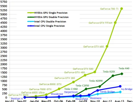
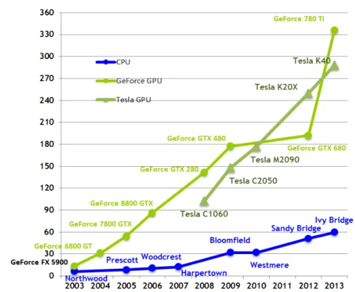
The use of GPU platforms is getting more and more general in the field of HPC and in real-time systems as well. The dominancy of these architectures versus the conventional CPUs are shown on Figure 1.5 and 1.6. In the beginning only the game and CAD industry was driving the chip manufacturers to develop more sophisticated devices for their needs. Recently, as these platforms have gotten more and more general to satisfy the need of different type of users, the GPGPU (General Purpose GPU) computing has evolved. Now the scientific community is benefiting from these result as well.
Figure 1.5: The increase in computation power. A comparison of NVIDIA GPUs and Intel CPUs. [20]
1.3.1.1 The NVIDIA CUDA architecture
CUDA is a combination of hardware and software technology [20] to provide program- mers the capabilities to create well optimized code for a specific GPU architecture that is general within all CUDA enabled graphics cards. The CUDA architecture is designed to provide a platform for massively parallel, data parallel, compute intensive applications.
The hardware side of the architecture is supported by NVIDIA GPUs, whereas the soft- ware side is supported by drivers for GPUs, C/C++ and Fortran compilers and the
Chapter 1. Introduction 12
Figure 1.6: The increase in memory bandwidth. A comparison of NVIDIA GPUs and Intel CPUs. [20]
necessary API libraries for controlling these devices. As CUDA handles specialised key- words within the C/C++ source code, this modified programming language is referred to as the CUDA language.
The programming model, along with the thread organisation and hierarchy and mem- ory hierarchy is described in [20]. A thread in the CUDA architecture is the smallest computing unit. Threads are grouped into thread blocks. Currently, in the Fermi and Kepler architectures maximum 1024 threads can be allocated within a thread block.
Thousands of thread blocks are organized into a block grid and many block grids form a CUDA application. This thread hierarchy with thread blocks and block grids make the thread organisation simpler. Thread blocks in a grid are executed sequentially. At a time all the Streaming Multiprocessors (SM or SMX) are executing a certain number of thread blocks (a portion of a block grid). The execution and scheduling unit within an SM (or SMX) is a warp. A warp consists of 32 threads. Thus the scheduler issues an instruction for a warp and that same instruction is executed on each thread. This procedure is similar to SIMD (Single Instruction Multiple Data) instruction execution and is called SIMT (Single Instruction Multiple Threads).
Chapter 1. Introduction 13 The memory hierarchy of the CUDA programming model can be seen in Fig. 1.7. Within a block each thread has its own register, can access the shared memory that is common to every thread within a block, has access to the global (graphics card RAM) memory and has a local memory that is allocated in the global memory but private for each thread. Usually the latter memory is used to handle register spill. Threads can also read data through the Read-Only Cache (on Kepler architecture) or Texture Cache (on Fermi architecture).
1.3.1.2 The Fermi hardware architecture
The CUDA programming architecture is used to implement algorithms above NVIDIA’s hardware architectures such as the Fermi. The Fermi architecture is realized in chips of the GF100 series. Capabilities of the Fermi architecture are summarized in [21].
The base Fermi architecture is implemented using 3 billion transistors, features up to 512 CUDA cores which are organized in 16 SMs each encapsulating 32 CUDA cores.
Compared to the earlier G80 architecture along with others a 10 times faster context switching circuitry, a configurable L1 cache (16 KB or 48 KB) and unified L2 cache (768 KB) is implemented. In earlier architectures the shared memory could be used as programmer handled cache memory. The L1 cache and the shared memory is allocated within the same 64 KB memory segment. The ratio of these two memories can be chosen as 16/48 KB or as 48/16 KB.
Just like the previous NVIDIA architectures, a read-only texture cache is implemented in the Fermi architecture. This cache is embedded between the L2 cache and ALU, see Fig. 1.7. Size of the texture cache is device dependent and varies between 6 KB and 8 KB per multiprocessor. This type of cache has many advantages in image processing.
During a cache fetch, based on the given coordinates, the cache circuitry calculates the memory location of the data in the global memory, if a miss is detected the geometric neighbourhood of that data point is fetched. Using normalized floating point coordinates (instead of integer coordinates) the intermediate points can be interpolated. All these arithmetic operations are for free.
Beside the texture cache the Fermi architecture has a constant memory cache (prior architectures had it as well). This memory is globally accessible and its size is 64 KB.
Constant data are stored in the global memory and cached through a dedicated circuitry.
Chapter 1. Introduction 14 It is designed for use when the same data is accessed by many threads in the GPU. If many threads want to access the same data but a cache miss happens, only one global read operation is issued. This type of cache is useful if the same, small amount of data is accessed repeatedly by many threads. If one would like to store this data in the shared memory and every thread in the same block wanted to access the same memory location, that would lead to a bank conflict. This conflict is resolved by serializing the memory access, which leads to a serious performance fall.
In Fermi NVIDIA introduced the FMA (Fused Multiply and Add) [21] operation using subnormal floating point numbers. Earlier a MAD (Multiply and Add) operation is performed by executing a multiplication. The intermediate result is truncated finally the addition is performed. FMA performs the multiplication, and all the extra digits of the intermediate result are retained. Then the addition is performed on the denormalised floating number. Truncation is performed in the last step. This highly improves the precision of iterative algorithms.
1.3.1.3 The Kepler hardware architecture
The Kepler generation [22] of NVIDIA GPUs has essentially the same functionality as the previous Fermi architectures with some minor differences. Kepler GPUs have a number of SMX (Streaming Multiprocessor – eXtended) functional units. Each SMX has 192 relatively simple in-order execution cores. These operate effectively in warps of 32 threads, so they can be thought of as vector processors with a vector length of 32. To avoid poor performance due to the delays associated with accessing the graphics memory, the GPU design is heavily multi-threaded, with up to 2048 threads (or 64 warps) running on each SMX simultaneously; while one thread in a warp waits for the completion of an instruction, execution can switch to a different thread in the warp which has the data it requires for its computation. Each thread has its own share (up to 255 32 bit registers) of the SMX’s registers (65536 32 bit registers) to avoid the context-switching overhead usually associated with multi-threading on a single core. Each SMX has a local L1 cache, and also a shared memory which enables different threads to exchange data. The combined size of these is 64kB, with the relative split controlled by the programmer.
There is also a relatively small 1.5MB global L2 cache which is shared by all SMX units.
Chapter 1. Introduction 15
Figure 1.7: Kepler and Fermi memory hierarchy according to [22]. The general purpose read-only data cache is known on Fermi architectures as texture cache, as historically it was
only used to read textures from global memory.
1.3.2 CPU: The Intel Sandy Bridge architecture
The Intel Sandy Bridge [23, 24] CPU cores are very complex out-of-order, shallow- pipelined, low latency execution cores, in which operations can be performed in a dif- ferent order to that specified by the executable code. This on-the-fly re-ordering is performed by the hardware to avoid delays due to waiting for data from the main mem- ory, but is done in a way that guarantees the correct results are computed. Each CPU core also has an AVX [25] vector unit. This 256-bit unit can process 8 single precision or 4 double precision operations at the same time, using vector registers for the inputs and output. For example, it can add or multiply the corresponding elements of two vectors of 8 single precision variables. To achieve the highest performance from the CPU it is important to exploit the capabilities of this vector unit, but there is a cost associated with gathering data into the vector registers to be worked on. Each cores owns an L1 (32KB) and an L2 (256KB) level cache and they also own a portion of the distributed L3 cache. These distributed L3 caches are connected with a special ring bus to form a large, usually 15-35 MB L3 or LLC (Last Level Cache). Cores can fetch data from the cache of another core.
Chapter 1. Introduction 16 1.3.3 MIC: The Intel Knights Corner architecture
The Intel Knights Corner [26] MIC architecture on the Intel Xeon Phi card is Intel’s HPC coprocessor aimed to accelerate compute intensive problems. The architecture is composed of 60 individual simple, in-order, deep-pipelined, high latency, high through- put CPU cores equipped with 512-bit wide floating point vector units which can process 16 single precision or 8 double precision operations at the same time, using vector regis- ters for inputs and output. Low level programming is done through the KNC (or IMCI) instruction set in assembly. This architecture faces mostly the same programmability issues as the Xeon CPU, although due to the in-order execution the consequences of inefficiencies in the code can result in more server performance deficit. The MIC copro- cessor uses a similar caching architecture as the Sandy Bridge Xeon CPU but has only two levels: L1 with 32KB and the distributed L2 with 512KB/core.
1.3.4 FPGA: The Xilinx Virtex-7 architecture
FPGA (Field Programmable Gate Array) devices have a long history stemming from the need to customize the functionality of the IC design on demand according to the needs of a customer, as opposed to ASIC (Application Specific Integrated Circuit) design where the functionality is fixed in the IC. An FPGA holds an array of CLB (Configurable Logic Block), block memories, customized digital circuitry for arithmetic operations (eg. DSP slices) and reconfigurable interconnect, which connects all these units. The function- ality (ie. the digital circuit design) of the FPGA is defined using the HDL (Hardware Description Language) languages like VHDL or Verilog. After the synthetization of the circuit from the HDL description the FPGA is configured using an external smart source. FPGAs come in different flavours according to the application area, such as network routers, consumer devices, automotive applications etc. The Xilinx Virtex-7 FPGA family [27] is optimized for high performance, therefore it has a large number of DSP slices and a significant amount of block RAM which makes it suitable for HPC applications.
Chapter 2
Alternating Directions Implicit solver
2.1 Introduction
Let us start the discussion of the ADI solvers with the numerical solution of the heat equation on a regular 3D grid of size 2563 – the detailed solution is discussed in Section 2.2. An ADI time-marching algorithm will require the solution of a tridiagonal system of equations along each line in the first coordinate direction, then along each line in the second direction, and then along each line in the third direction. There are two important observations to make here. The first is that there are 2562 separate tridiagonal solutions in each phase, and these can be performed independently and in parallel, ie. there is plenty of natural parallelism to exploit on many core processors. The second is that a data layout which is optimal for the solution in one particular direction, might be far from optimal for another direction. This will lead us to consider using different algorithms and implementations for different directions. Due to this natural parallelism in batch problems, the improved parallelism of CR (Cyclic Reduction) and PCR (Parallel Cyclic Reduction) are not necessarily advantageous and the increased work-load of these methods might not necessarily pay off. If we take the example of one of the most modern accelerator cards, the NVIDIA Tesla K40 GPU, we may conclude that the 12GB device memory is suitable to accommodate aNdmultidimensional problem domain with Nd= 12 GB/4 arrays = 0.75×10⁹ single precision grid points – assuming 4 arrays (a,b,c
17
Chapter 2. Alternating Directions Implicit solver 18 and d) are necessary to store and perform in-place computation of tridiagonal system of equations as in Algorithm 1. This means that the length N along each dimension is N = √d
0.75×10⁹ for dimensionsd= 2−4 as shown on Table2.1.
d N # parallel systems
2 27386 27386
3 908 824464
4 165 4492125
Table 2.1: Number of parallel systems increases rapidly as dimensiond is increased. N is chosen to accommodate anNdsingle precision problem domain on the available 12 GB of an
NVIDIA Tesla K40 GPU.
The ADI (Alternating Direction Implicit) method is a finite difference scheme and has long been used to solve PDEs in higher dimension. Originally it was introduced by Peaceman and Rachford [14], but many variant have been invented throughout the years [15, 16, 9]. The method relies on factorization of the spatial operators: approximate factorization is applied to the Crank-Nicolson scheme. The error introduced by the factorization is second order accurate in both space (O(∆x2) and time (∆t2)). Since the Crank-Nicolson is also second order accurate, the factorization conserves the accuracy.
The benefit of using ADI instead of other (implicit) methods is the better performance.
Splitting the problem this way changes the sparse matrix memory access pattern into a well defined, structured access pattern. In case of the Crank-Nicolson method a sparse matrix with high (matrix) bandwidth has to be handled.
Solving the tridiagonal systems can be performed either with the Thomas (aka. TDMA - Tridiagonal Matrix Algorithm) 3.2.1, Cyclic Reduction (CR) 3.2.2, Parallel Cyclic Reduction (PCR)3.2.3, Recursive Doubling (RD) [28] etc. In engineering and financial applications the problem size is usually confined in a Nd hypercubic domain, whereN is typically in the order of hundreds.
2.2 Solving the 3D linear diffusion PDE with ADI
The exact formulation of the ADI method used in the dissertation is discussed through the solution of a three dimensional linear diffusion PDE, ie. the heat diffusion equation
Chapter 2. Alternating Directions Implicit solver 19 withα= 1 thermal diffusivity, see Eq.(2.1).
∂u
∂t =∇2u (2.1)
or
∂u
∂t = ∂2
∂x2 +∂2
∂y2 +∂2
∂z2
u (2.2)
where u = u(x, y, z, t) and u is a scalar function u : R4 7→ R, x, y, z ∈ R are the free spatial domain variables and t∈Rfree time domain variable.
In brief: splitting the spatial, Laplace operator is feasible with approximate factorization.
The result is a chain of three systems of tridiagonal equations along the three spatial dimensions X,Y and Z. The partial solution of the PDE along the dimension X is used to compute the next partial solution of the PDE along the Y dimension and then the solution of Y is used to solve the partial solution in Z dimension. The formulation of the solution presented here computes the contribution ∆u which in the last step is added to the dependent varaible u.
The formulation starts with the Crank-Nicolson discretization, where a backward and forward Euler discretization is combined with the trapezoidal formula with equal 1/2 weights, see Eq.(2.3). Due to the backward Euler discretization ADI is an implicit method central difference spatial discretizations (Crank-Nicolson discretization):
un+1ijk −unijk
∆t = 1
2 1
h δ2x+δy2+δz2
un+1ijk +1
h δx2+δ2y+δ2z unijk
(2.3) here (x, y, z) ∈ Ω = {(i∗∆x, j∗∆y, k∗∆z)|i, j, k = 0, .., N−1;h= ∆x= ∆y= ∆z}, t=n∗∆tand δx2unijk =uni−1jk−2unijk+uni+1jk is the central difference operator.
Fromun+1ijk =unijk+ ∆uijk and Eq.(2.3) it follows that
∆uijk =λ δx2+δy2+δz2
2unijk+ ∆uijk
(2.4)
whereλ= ∆th .
∆uijk−λ δx2+δy2+δz2
∆uijk = 2λ δx2+δy2+δz2
unijk (2.5)
Chapter 2. Alternating Directions Implicit solver 20 1−λδx2−λδy2−λδ2z
∆uijk= 2λ δx2+δ2y+δ2z
unijk (2.6)
Eq.(2.6) is transformed into Eq.(2.7) by approximate factorization. One may verify the second order accuracy of Eq.(2.7) by performing the multiplication on the LHS.
1−λδx2
1−λδy2
1−λδ2z
∆uijk = 2λ δx2+δ2y+δ2z
unijk (2.7)
The solution of Eq.(2.7) above boils down to performing a preprocessing stencil operation Eq.(2.8), solving three tridiagonal system of equations Eqs. (2.9),(2.10) and (2.11) and finally adding the contribution ∆u to the dependent variable in Eq.(2.12).
u(0)= 2λ δx2+δy2+δz2
unijk (2.8)
1−λδx2
u(1)= u(0) (2.9)
1−λδy2
u(2)= u(1) (2.10)
1−λδz2
∆uijk= u(2) (2.11)
un+1ijk = unijk+ ∆uijk (2.12)
where u(0),u(1),u(2) denote the intermediate values and not time instance. Eq.(2.13) represents the solution with tridiagonal system of equations.
u(0)ijk=2λ
uni−1jk+uni+1jk+ unij−1k+unij+1k+ unijk−1+unijk+1
−6unijk
axijku(1)i−1jk+bxijku(1)ijk+cxijku(1)i+1jk =u(0)ijk ayijku(2)ij−1k+byijku(2)ijk+cyijku(2)ij+1k=u(1)ijk azijk∆uijk−1+bzijk∆uijk+czijk∆uijk+1=u(2)ijk
un+1ijk =unijk+ ∆uijk
(2.13)
Chapter 2. Alternating Directions Implicit solver 21 Note that the super and subscript indices of coefficientsa,b and cmean that the coef- ficients are stored in a cubic datastructure.