Development and characterisation of silicon microfluidic components and
systems
PhD Thesis
Zoltán Fekete
Supervisor: Péter Fürjes, PhD
MEMS Lab, Institute for Technical Physics and Materials Science Research Centre for Natural Sciences, Hungarian Academy of Sciences,
MTA TTK MFA
2012
2
Content
1. Preface ...3
1.1 Motivation and goals ...3
1.2 Structure of dissertation ...4
2. Microfluidics and biomedical applications ...5
2.1 Introduction to microfluidics ...5
2.2 Drug delivery in neural applications...7
2.3 Blood as sample analyte ...9
2.4 Sample preparation in microfluidic systems...8
3. Fabrication of silicon microfluidic systems ... 13
3.1 Introduction to MEMS technology ... 13
3.2 Role of MEMS technology in microfluidics ... 14
3.3 Deep Reactive Ion Etching... 15
3.4 Microchannels in silicon MEMS ... 18
4. Development and characterisation of drug delivery system for Si microprobes ... 22
4.1. History & advances in silicon microprobe technology ... 22
4.2 Development of drug delivery system in silicon microprobes ... 25
4.2.1 Fabrication of buried microchannels ... 25
4.2.2 Fabrication parameters vs. microchannel shape ... 30
4.2.3 Integration into neural microprobes ... 33
4.3 Mechanical performance of Si microprobes ... 35
4.3.1 Impacts during medical implantation ... 35
4.3.2 Experimental methods ... 37
4.3.3. Fracture test results ... 39
4.3.4. In vivo results ... 43
4.4. Characterisation of integrated drug-delivery system ... 47
4.4.1 Terminology ... 47
4.4.2 Experimental methods ... 48
4.4.3 Hydrodynamic characterisation ... 50
4.4.4 In vivo results ... 52
5. Development of sample preparation microfluic system ... 54
5.1. Recent advances in microscale blood separation ... 54
5.1.1. Overview of blood separation methods ... 54
5.1.2 Principle of Zweifach-Fung separation ... 56
5.2. Characterisation of Zweifach-Fung separation method ... 57
5.2.1. Experimental methods... 57
5.2.2. Performance of single bifurcations ... 61
5.3 Optimisation and integration of Zweifach-Fung separation method ... 64
5.3.1. Cascade-type bifurcation based separation system ... 64
5.3.2. Towards the Lab on a Chip ... 65
6. Overview of scientific results ... 70
7. Utilization of scientific results ... 72
8. References ... 73
9. List of publication ... 81
10. Acknowledgement ... 84
11. List of acronyms ... 85
12. Appendices ... 86
3
1. Preface
1.1 Motivation and goals
Recently, the role of microfluidics in biomedicines is steadily increasing. Due to latest progress in micro- and nanotechnology potential clinical applications are expected to be fulfilled in the near future. In my work, microfluidic research focuses on the areas of neuroscience and medical diagnostics, where my investigation on both microfabrication and physical principles can further improve reliable design of microcomponents and devices in these promising fields.
Neuroprosthetics
By aging of the society, brain-related clinical cases like paralysis, epillepsy or Parkinson diseases are remarkably increasing acting as critical issues to be solved for today medicine. Medical attendance and rehabilitation of such diseases is very challenging for both patients and their relatives. The aim of modern neurophysiology is to improve their quality of life. Processing of signals generated by brain neurons is of great importance in neurophysiology, since a large amount of information can be gained about the dynamics of the nervous system and the relationship between brain and motor function activity [1.1]. As a result of efforts in this field, a wide range of structural material like silicon has been used to fabricate probes, which is applicable to record the activity of brain cells in non-human experiments extending our knowledge about the above issues.
Researchers have used pharmacologic intervention (e.g. systematic injection) anti- inflammatory agents can be transported via microfluidic systems into the tissue around the microprobes, and noticed that the response of neighbouring cells and neural tissues changed. Drug delivery in acute experiments can be easily implemented, however, during chronic implantation, the local injection of drugs is more critical. The advantages of the latter is that smaller amount of biological sample is necessary, cells can be directly excited, while peripheral metabolism and the reactive response of neural tissue is excluded increasing the long-term stability of the device [1.2].
My goal in the field of neural microdevices was to design and realise multi- functional microprobes integrating a parallel system of electric sensing or excitation and local drug delivery functions into a single substrate. Since the characterisation of the mechanical and fluidic properties of microprobes fabricated by the proposed technology are essential for future application, and a number of in vivo experiments has been carried out to evaluate microprobe performance.
Diagnostics of blood
Currently, cardiovascular diseases are among the leading reasons of casualties worldwide. Almost every third fatal occasion originates from such illnesses. Fast diagnostics are essential to anticipate the deterioration of several diseases. Therefore, the research and development of microanalytical systems (Lab-on-a-chip, µTAS – micro-Total-Analysis-System) are increasingly heading toward the downscaling and cost-effective fabrication of today’s medical microdevices [1.3]. Such systems are able
4
to complete complex analytical tasks or perform personalized diagnosis that demanded the presence of serious hardware or professional personnel before. In the microscale not only the adaptation of analytical principles means great challenge, but the transport and preparation of biological samples are still relevant issues. Since hydrodynamic phenomena are often different than in the macroscopic world, the solution of sample manipulation (extraction, dilution, separation, and transport to the active region) is a great challenge for microengineers of micro- and nanofluidic systems [1.4].
The aim of the vast majority of clinical tests is the detection of the presence and quantity of several proteins, ions, crystalloids or diluted gas in blood plasma. Since the cell components of blood are not desired during measurements, the first step is removing these particles from the blood plasma. If the measurements are to be embedded in a microsystem, the integration of separation is important [1.5].
The presence of proteins can be efficiently identified by solid-state nanopore membranes as sensing elements. Nanopore sensing is an extremely sensitive analytical method due to the nanoscale pore geometry (shape and surfaces), which makes the interactions between pore surface and molecules of analytes to contribute to the control of ion or molecule transport [1.6]. The detection principle is based on the selective interaction of pores and the analysed component which reduces the permeability of nanopores for the measured marker ions or molecules, and therefore produces a flux change equivalent to the analytical signal. Sensitivity is outstanding, since extremely small immobilized component causes apparent modulation in ion or molecule flux.
My goal in the field of diagnostics of cardiovascular diseases was to design and realise a silicon based microfluidic system, which contains the functions of sample preparation as well as the sensing element. To prepare whole blood, plasma separation and dilution has to be optimized in the microscale and the integration of a detection unit highly sensitive to blood proteins has to be implemented in a single microsystem. This way a rapid diagnosis can be set up in the case of diseases demanding fast intervention (e.g. stroke) in situ [1.7].
1.2 Structure of dissertation
In my thesis, I will give a deeper insight into novel scientific results in microfluidics and related issues. I achieved my work in the MEMS Laboratory of the Institute for Technical Physics and Material Science. This PhD thesis is organized as follows.
In Chapter 2, I introduce the reader to the background of my motivation in the fields of neural implants and Lab-on-a-chip systems.
Chapter 3 contains a brief description on state-of-the-art fabrication principles and technology in microengineering sciences. A general overview of literature on the advanced technologies of silicon based microfluidic components and devices support a better comprehension of following chapters on microfabrication.
In Chapter 4, my proposed fabrication technology and integration of sealed microfluidic channels in silicon into silicon probes are presented, followed by fluidic and mechanical characterisation of the realised microprobes.
In Chapter 5, the principle, characterisation and optimization of a microfluidic sample preparation function is described, and integration concept into Lab-on-a-chip devices is presented.
5
2. Microfluidics and biomedical applications
2.1 Introduction to microfluidics
By definition microfluidics is the science and engineering of systems in which fluid behaviour differs from conventional flow theory primarily due to the small dimensions of the system. According to other explanations, microfluidics generally deals with the behaviour, precise control and manipulation of fluids that are geometrically constrained to a small, typically sub-millimetre scale. Microfluidics is undoubtedly a multidisciplinary field intersecting engineering, physics, chemistry, microtechnology and biotechnology, with practical applications to the design of systems in which such small volumes of fluids will be used. Microfluidics emerged in the beginning of the 1980s and is used in the development of inkjet print heads, DNA chips etc.
Besides small device size, in this regime typical system parameters results in smaller volume of fluids to be handled and lower energy consumption is needed, however, the physical effects typical of the micro domain emerges and should be considered during the design of individual components. Most of the applications include passive microfluidic control like capillary forces, while a number of other devices are equipped external or integrated actuators (e.g. microvalves and micropumps) for providing fluid transport. Latter ones are called active microfluidic systems.
Microfluidic components and systems have several advantages which are attributed to miniaturization:
Small volume of analyte is necessary
Speed of reaction is increased
Precise manipulation (mixing, separation, heating etc) is available
Other devices can be integrated (Lab-on-a-chip - LOC)
Disposable assays and cartridges can be used
Cost of reagents are reduced
High surface to volume ratio
Dead volume s minimized
More parameters can be monitored simultaneously
As mentioned above, micro level brings dramatic changes in the impact of several physical effects [1.8]. Analyzing the physical properties of microsystems is expressive if the concept of scaling laws is applied. A scaling law describes the variation of physical quantities with the size of the given system or object, while keeping other quantities such as time, pressure, temperature, etc. constant. As an example, consider volume forces, such as gravity and inertia, and surface forces, such as surface tension and viscosity. The basic scaling law for the ratio of these two classes of forces can generally be expressed by
6
3 0
2 1
l volume
surface
l l l F
F (2.1)
This scaling law implies that when scaling down to the microscale in lab-on-a-chip systems, the volume forces, which are very prominent in our daily life, become largely unimportant.
At the microscale some other interesting and sometimes unintuitive properties also appear. In particular, the Reynolds number, which described in more details in Chapter 4.4.1., can become very low. A key consequence of this is that fluid flow is generally laminar, and do not necessarily mix in the traditional sense (see Fig. 2.1); molecular transport happens often through diffusion. High specificity of chemical and physical properties (concentration, pH, temperature, shear force, etc.) can also be ensured resulting in more uniform reaction conditions and higher grade products in single and multi-step reactions.
Figure 2.1: Laminar flow of water (buffer) and fluorescently labelled human serum albumine (HSA) in a T-type micromixer (a.) and hydrodynamic particle focusing with
three flow stream (b.) produced in the MEMS Lab of TTK MTA MFA.
The basis of most LOC fabrication process is photolithography. Initially most of the processes are in silicon, as these well-developed technologies are directly derived from semiconductor fabrication. Because of demands for e.g. specific optical characteristics, bio- or chemical compatibility, lower production costs and faster prototyping, new processes have been developed such as glass, ceramics and metal etching, deposition and bonding, polydimethylsiloxane (PDMS) and SU-8 processing (e.g., soft lithography - see Fig. 2.2), thick-film- and stereolithography as well as fast replication methods via electroplating, injection moulding and embossing. Furthermore the LOC field more and more exceeds the borders between lithography-based microsystem technology, nanotechnology and precision engineering. My work focuses on some highlights of silicon based microfabrication.
a. b.
7
Figure 2.2: Moulding form in SU-8 for Rapid Prototyping (a.) and moulded PDMS based Lab-on-a-chip (b.) produced in the MEMS Lab of TTK MTA MFA.
2.2 Drug delivery in neural applications
The development of pharmacological functions in neural applications is definitely inspired by Deep Brain Stimulation (DBS) techniques [2.1]. Since blood-brain barrier is not penetrable for most proteins, localised delivery of e.g. growth factors is preferred.
The idea of treating neurologic disorders with chronic stimulation began to emerge in the 1960s, but stimulation was largely used for targeting surgical lesions. At the end of 1960s a method of chronic implantation of a bundle of multiple electrode wires deep in the brain was developed. The goal of the stimulation was to delineate the “best”
target for a subsequent lesion. Although the goal was initially the lesion guidance only, the period of chronically implanted electrodes started. Since then, DBS has become increasingly used for treating a variety of disorders. As a result of progress in the field of microengineering, implantable neural electrodes with the ability of simultaneous chemical stimulation and electrical recording have been fabricated and applied. They offer interesting perspectives for a variety of common and severe health problems e.g.
hearing loss [2.2], chronic pain [2.1, 2.3], essential tremor [2.1], Parkinson [2.1]
diabetes [2.3], Alzheimer [2.4], depression [2.5] or epilepsy [2.6]. Simultaneous chemical and electric interactions with the very same groups of cells of an active brain might induce a huge progress in these studies. Moreover, the long-term stability of electrophysiological implants is to be enhanced. With the help of continuous dosage of anti-inflammatory drugs, delaying or reducing the response of the surrounding tissue might be also possible [2.7-2.8]. Currently, the development of microsystems for neural application focuses on the solution of the above issues to maintain the dynamics of progress in this discipline.
As far as the implantation apparatus is concerned, wire electrodes for recording and stimulation of electrical signals [2.9] as well as glass or steel capillaries used to deliver pharmaceutical substances directly into the brain [2.10] are the established tools in neuroscience research. However, the rapid development of micro-electromechanical systems (MEMS) within the last decades has opened completely new technological perspectives with respect to system integration of advanced functions [2.11]. A detailed description of recent progress on microprobe technology is presented in Chapter 4.
a. b.
8
The application and optimization of microfluidic principles in neural drug delivery system is still in its infancy. Novel techniques could take further roles in biomedical devices, if their comprehensive characterisation took place after preliminary demonstrations. The mission of microtechnology regarding neural implants is now to review, optimize and integrate the latest developments of microfluidic researches in order to make reliable and efficient physiological and pharmacological measurements through neural implants. My aim is to develop and optimize a microchannel fabrication technology and integrate it into a neural microprobe. Since the fluidic and mechanical performance of a hollow microprobe is significantly affected by the integrated channel system, these issues are also addressed experimentally in later chapters.
2.3 Sample preparation in microfluidic systems
The entire volume of human blood is recirculated throughout the body in every minute. It delivers oxygen and nutrients to every cell and transports products from and toward tissues. During this recirculation, cells of the immune system are also transported quickly and efficiently through blood performing specific immuno- surveillance functions where necessary. As a result, blood can give large amount of information on the actual state of all tissues and organs. This implies that blood sampling and analysis are of great interest for both medical and science applications, and hold a central role in the diagnosis of many physiologic and pathologic conditions.
Progress in technology facilitated several breakthroughs in extending our knowledge on biology and inherently blood itself [2.12]. Advances in microscopy by the seventeenth century allowed the observation of individual cells in blood. Later, in the nineteenth century, the development of tissue-staining techniques facilitated the characterisation of the first blood cell populations. The most common and yet the most informative examination in haematology is performed by Wright-Giemsa staining procedures and full blood count [2.13]. Staining procedures utilize histological stain that facilitates the differentiation of several blood cell types, while counting methods are based on flow cytometry techniques.
Flow cytometry techniques represent nowadays the golden standard in cell identification and separation producing finer details and higher throughput than previous techniques. However, as complexity of these latest techniques is getting higher, they require increasingly higher levels of skill of users. The analysis of the cellular component in particular has been affected by restricting it to highly specialized and strictly regulated laboratories, to the detriment of point-of-care diagnostic tools. In spite of strict regulations, a large number of blood handling is still performed manually, even in relatively well automated laboratories, or in conditions that may significantly alter the results of subsequent analysis. Efforts to reduce the chance for emerging errors, to reduce time blood is exposed from collection until analysis and to increase availability of state-of-the-art analysis techniques on the premises and at low cost requires a completely new approaches.
As new technologies emerge in biological applications, microfluidics and microscale lab-on-a-chip-type devices are getting into the focus of blood analysis development [2.14]. Availability of health care and diagnostics at the bedside is often referred to as point-of-care testing (POCT). Through POCT analysers clinical diagnostics will certainly be revolutionalised. New devices for convenient use at home or in doctors’ offices would allow for rapid and accurate diagnostic and prognostic, based on blood cells, of infectious diseases, cancers, and inflammatory responses. As a
9
result, a better matching between drugs and patient pathophysiology is expected, reducing side effects and improving efficiency of therapy.
In the field of drug discovery, microfluidic devices can redefine the entrance criteria for clinical trials and examine for these criteria sparing time and costs.
Moreover, microfabricated devices for sample preparation would open up new possibilities by facilitating comprehensive genomic and proteomic analysis from even small homogenous subpopulations down to single cells. Generally, blood sample preparation in lab-on-a-chip systems may result more gentle, fast, and consistent manipulation of living cells, and therefore produce better quality of gained information.
Due to the rapid development of microfabrication principles, a large number of manipulation technique come to exist, however, only a few of them has been extensively characterised regarding performance, feasibility or possible integration into lab-on-a-chip systems. My aim is to provide a deeper insight into blood plasma separation techniques, and describe the experimental characterisation and optimization of the so-called Zweifach-Fung particle separation method, which will be explained in details in Chapter 5.
2.4 Blood as sample analyte
In this section, I give a brief overview on the physical properties of blood, focusing on characteristic phenomena essential to have knowledge of in order to see the issues during manipulation of blood.
Composition of blood
Approximately eight percent of the total weight of human body is composed of blood. Its average density is 1060kg/m3 and dynamic viscosity is 0.005Pas, which is very close to that of water (1000kg/m3 and 0.001Pas respectively). An adult person generally has a volume of blood of 5l, which eventually the mixture of plasma, proteins, lipids and several cell components. Traditionally the separation of plasma from cells takes place by centrifuging. This way, the produced plasma consists of 90% water, 7%
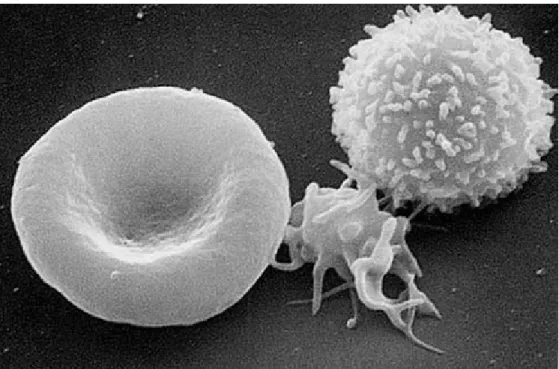
plasma proteins, 2% organic and 1% inorganic materials. Cell components are mainly erythrocytes or red blood cells (RBC), leukocytes or white blood cells (WBC), and thrombocytes or platelets (see Fig. 2.3). White blood cells responsible for immunological mechanisms and platelets responsible for thrombosis constitutes only 1/600 and 1/800 part of the whole cell quantity respectively. RBC constitutes almost 45-50% of whole volume of blood. Approximately, there is 5*106 RBC per mm3. Besides, the average number of WBC is 5-8 thousand per mm3, while the number of platelets is between 250-300 thousands per mm3.
10
Figure 2.3: A three-dimensional ultrastructural SEM image of a T-lymphocyte (right), a platelet (centre) and a red blood cell (left) made in The National Cancer
Institute at Frederick.
Characteristic hydrodynamic and rheological properties of blood can attributed to RBC because of their dominant presence in whole blood. RBC can be considered as biconcave discs. Their diameter is around 7-8µm, their thickness is ~3µm at the circumference and 1µm at the centre. This special biconcave shape is responsible for the little change in surface area even during considerable deformations.
Dilution of blood
Particle concentrations of blood samples are often referred as haematocrit value, which is the volumetric density of RBC. The average haematocrit value is 40-52% and 35-47% in case of adult men and women respectively.
In case of blood samples at rest, RBCs and platelets start to coagulate. This mechanism is called as thrombosis, which is caused by fibrinogen proteins in blood plasma. Since coagulation is an unwanted phenomenon during rheological experiments, blood samples are generally diluted by heparin, EDTA or citrate in order to avoid thrombotic reaction. This way the natural composition of blood is inherently modified, therefore it is essential to carry out blood separation and analysis as fast as possible.
J Zhang et. al. [2.15] have tested how the haematocrit value affects the separation efficiency (more detailed in Chapter 5). Their results are shown in Fig. 2.4. They proposed that separation efficiency increases significantly at low haematocrit value;
therefore a preliminary dilution is recommended and eventually used in my experiments.
11
Figure 2.4: Separation efficiency plotted against the sample haematocrit value [2.15]
Viscosity of blood
Fluids, in which the relationship between velocity gradients and shear forces is directly proportional, are called Newtonian fluids. Because of its hydrodynamic properties, blood plasma is also considered as Newtonian fluid [2.16]. However, cells definitely increase blood viscosity (see Fig. 2.5), which depends on flow velocity, microchannel cross-section parameters, density of cells and temperature as well. Whole blood (plasma and cells altogether) therefore shows non-Newtonian behaviour, which finally contributes the easier flow through small capillaries or vessels than plasma itself.
Figure 2.5: The diagram shows the relationship between capillary diameter (x-axis) and viscosity (y-axis). It is clear that at low haematocrit value almost no change in viscosity can be noticed when the tube diameter decreases.
As it is illustrated on Fig. 2.5, blood viscosity is also influenced by microcapillary geometry (e.g. tube diameter). In small capillaries viscosity decreases significantly when decreasing tube diameter. In literature this phenomenon is also referred as Fahraeus-Lindqvist effect.
12
In the case of small deformations, blood viscosity is constant. When increasing shear velocity (gradient of flow velocity), viscosity is decreasing until a constant plateau is reached. Materials are called pseudoelastic, if increasing deformation causes lower viscosity. This property is triggered by the presence of RBC and physical explanation is based on their flexibility and orientation in flow direction.
Haemolysis
Cells cannot be exposed to arbitrary shear forces, since above a critical value cell membrane is damaged, and intracellular content can enter the plasma. This so- called haemolysis is a negative effect in experiments. Cytoplasm alters the composition and ion concentration of blood plasma. Additionally, such proteins can get into blood flow that is usually observed in the plasma only in diseased cases. This way an artefact in analytical measurements can be present. By a precise design of device operation parameters, haemolysis can be avoided. Fig. 2.6 shows the haemolysis index (derived from photometric plasma-haemoglobin measurements) plotted against shear stress and exposition time. Exposition time is the period of time until the cells were exposed to a certain shear load. Damage of RBC is negligible in a wide range, however in case of τ <
425Pa and texp > 620ms, it can be significant [2.17]. Microchannel sizing and initial flow velocity of blood should be chosen such that shear stresses stay below these experimentally defined critical values.
Figure 2.6: Haemolysis index plotted against shear stress and exposition time [2.17].
13
3. Fabrication of silicon microfluidic systems
3.1 Introduction to MEMS technology
MEMS (Micro-electro-mechanical systems) are referred as integrated devices or systems that combine electrical and mechanical components. They range in size from the submicrometre level to the millimetre level. The construction of MEMS devices extends the fabrication techniques developed for the integrated circuit industry to add mechanical elements such as beams, gears, diaphragms and springs to devices.
The three characteristic features of MEMS fabrication technologies are miniaturization, multiplicity and microelectronics. Miniaturization enables the production of compact and rugged devices with quick response times. Multiplicity refers to the batch fabrication inherent in semiconductor processing which allows thousands or millions of components to be easily and concurrently fabricated.
Microelectronics provides the intelligence to MEMS and allows the monolithic merging of sensors, actuators and analogue circuitry to build closed-loop feedback components and systems. IC fabrication technology or microfabrication has so far been the primary enabling technology for the development of MEMS. Advances in IC technology in the last decade have brought corresponding progress in the MEMS fabrication processes.
Manufacturing processes allow for the monolithic integration of MEMS structures with driving, controlling and signal processing electronics. This integration promises to improve the performance of micromechanical devices as well. The primary enabling technology for the development of MEMS is based on IC fabrication technology or microfabrication.
The major steps in IC fabrication technology are film growth, doping, lithography, etching, wafer bonding, dicing, and packaging.
Film growth: Usually, a polished Si wafer is used as the substrate, on which a thin film is grown. The film, which may be epitaxial Si, SiO2, silicon nitride (Si3N4), polycrystalline Si (polysilicon), or metal, is used to build both active or passive components, masking, dielectric or passivation layers as well as conduction bands or interconnections between circuits.
Doping can be used to modulate the physical properties of the device layer. Low and controllable level of an atomic impurity may be introduced into the layer by thermal diffusion or ion implantation, which is also useful as etch-stop layer for selective chemical etching of the substrate.
Lithography: A pattern on a mask is transferred to the film by means of a photosensitive (i.e., light sensitive) chemical known as a photoresist. The process of pattern generation and transfer is called photolithography. A typical mask consists of a glass plate coated with patterned chromium (Cr) film and positioned above the wafer by mask aligning systems.
Etching is the selective removal of unwanted regions of a film or substrate for pattern delineation. Wet chemical etching or dry etching may be used. Etch- mask materials are used at various stages in the removal process to selectively prevent those portions of the material from being etched. These materials include SiO2, Si3N4 or hard-baked photoresist.
14
Wafer bonding is applied to form closed microsystems by attaching silicon and/or glass substrates to one another.
Dicing: The finished wafer is sawed or machined into small squares, or dice, from which individual microchips can be made.
Packaging: The individual sections are then packaged, a process that involves physically locating, connecting, and protecting a device or component. MEMS design is strongly coupled to the packaging requirements, which in turn are dictated by the application environment. The concept of System-in-Package facilitates to integrate a wide range of functions into the same microcomponent as well.
A more detailed description of process steps of MEMS technology is presented in [3.1].
3.2 Role of MEMS technology in microfluidics
In the 1970s when integrated circuit technology has been adapted for the fabrication of physical sensors e.g. force or pressure sensors initiating the advent of MEMS era, there was no technical obstacles in making the first simple microfluidic systems as well. The first miniaturized gas chromatography system was realised around 1975 [3.2]. The proposed device circulated gas through microchannels etched in silicon and also contained electromagnetic injection as well as thermal detection, all on a single chip just a few centimetres wide. However, the needs of such developments have not been in the focus of those involved in silicon technology, therefore this achievement was individual attempt in that period [3.3]. Only at the beginning of the 1990s got the advantages of miniaturization into the spotlight. Once again all started with chromatography applications [3.4], and then all sorts of microfluidic systems began to be fabricated in a quick pace. Just a few examples from the many almost in chronological order were electrophoretic separation systems, [3.5], electroosmotic pumping systems [3.6], diffusive separation systems [3.7], micromixers [3.8], DNA amplifiers [3.9-3.10], cytometers [3.11], and chemical microreactors [3.12].
In parallel, microfluidics was being used to answer fundamental physical questions, e.g. first experiments involving the stretching of DNA [3.13] in 1993 and molecular level investigation has been triggered and lasts even today.
The first microfluidic products commercialized on a large scale were inkjet printer heads. By parallelizing ejection heads, droplet dispensers can also be constructed and can be successfully used for chemical or biological analyses. Droplet dispensers at this time constitute a substantial part of commercial activity in the field of microfluidics [3.14].
Today’s microfluidics chips are produced by the millions for chemistry and biology. The advantage of these chips is that they allow a massive number of tests to be run in parallel, and also provide large amounts of data, which is essential to precisely characterise a product. This kind of development is inevitably in the search for new types of medical treatments.
Due to the relative ease and accessibility of many of silicon based technologies, it has become possible to integrate several elements on the same chip and to create Lab-
15
on-a-chip devices. The rapid expansion of the field of microfluidics seems to be driven in part by the possibility of integration. The ultimate goal is to be able to detect biological molecules, and transport, mix and characterize a raw sample, all with one device. In traditional genomic analyses, it was necessary to purify and amplify a DNA fragment prior to analysis. This pre-treatment required complex laboratory and highlights the advantage of being able to integrate all these procedures on one chip to make it possible to directly analyse a raw sample, such as a drop of blood. Achieving this would require miniaturizing systems such as cytometers, separators, and bioreactors, and then together. The domain of integrated analysis systems has been designated as µTAS (micro-total analysis systems) [3.14], or also Lab-on-a-chip (LOC) systems. The two terms are essentially synonymous. Lab-on-a-chip devices or µTAS delineate an abundant field that includes analysers of air and water quality, diagnostics of illnesses, and medical implants etc. The economic possibilities of this field have been estimated at tens of billions of dollars per year
3.3 Deep Reactive Ion Etching
Deep reactive ion etching (DRIE) is a key technology of recently fabricated microfluidics and a deeper insight into the physical phenomena is essential to understand ideas in later paragraphs, therefore in the following section a detailed description is provided.
Dry or plasma etching is a group of chemical processes, where the etching medium is produced by the dissociation and ionization of stable molecules or atoms, or through the formation of chemically active particles. The chemical manner of the process is determined such that the etching medium and the etched substrate constitute a volatile reaction product. This etch process has two significant advantages compared to wet etching. The generation of extremely reactive components (see Fig. 3.1) in the plasma (chemical etch), the etch rates are remarkably higher and due the possibility of directional etching, more complex 3D microstructures can be formed.
Figure 3.1: Main phenomena taking place in plasma [3.1]
The directionality of etching (referred to as physical etching) is resulted by the presence of ionized particles in the plasma, which are moved towards the wafer surface
16
through controlled electric field in the system. In special cases, chemical etching and anisotropic physical etching are performed in a synergetic manner intensifying the effect of one another. Therefore, etch rates higher than the sum of etch rate of individual components can be achieved.
Currently the most important dry etching process is the reactive ion etching (RIE), where the following sub-processes take place respectively.
Generation of active particles from gas phase by ionization and dissociation of molecules in plasma glow. Active particles can be neutral species, electrons, protons, photons, free radicals or ions.
Evolution of DC self-bias. Silicon wafer is placed on a capacitively coupled electrode driven by radiofrequency source. Since electron mobility is greater than that of ions, the electrode becomes negatively charged, also called as DC self-bias (see Fig. 3.2).
Transport of neutral active radicals and positive ions from the plasma to wafer surface. Transport of radicals take place through diffusion, and ions are driven by DC-bias.
Adsorption. Reactive species are immobilized on the surface of silicon wafer. Adsorption can be enhanced by ion bombardment, which removes the reaction product passivating Si surface.
Reaction. Chemical reaction is to happen between adsorbed radicals and Si.
Desorption. By-product should be volatile in order to transport into gas phase (high partial vapour pressure on substrate temperature). In some cases, additional ion bombardment can be carried out to remove them.
Venting. Desorbed reaction product are diffused from the etched surface into the plasma, therefore they should be removed.
Figure 3.2: Potential distribution in plasma [3.1]
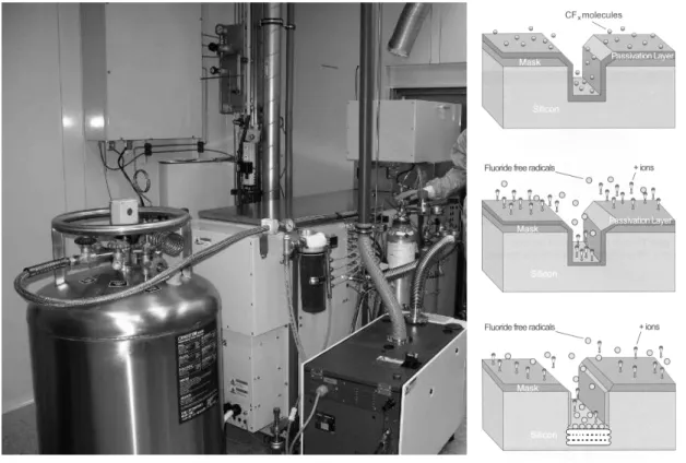
Etching of silicon takes place in halogen-based plasma because of the higher available etch rate. Gases generally used in DRIE systems are bromine, chlorine or fluorine. In the system I have worked with (Oxford Plasmalab 100 – see Fig. 3.3) fluorine based chemistry is used, which guarantees high etch rate, but limited anisotropy compared to bromine or chlorine. To increase the directionality of etching mechanism, ion-inhibitor techniques are applied. Etch stopping by-products deposited on the wafer surface are called inhibitors.
17
Most of today’s DRIE systems are equipped by two energy source, one dedicated to generate plasma, and one used for controlling the translation of generated ions toward the wafer surface. The first source is usually inductively coupled (ICP), while later one is capacitively coupled. This way the density of free radicals and ions in plasma, and energy of ion bombardment can be tuned in independent manner.
During ion-inhibitor procedures, the inhibitor film is necessary to control directionality of etching. The sidewall of etched structures are less exposed to the effect of ion bombardment, therefore the film is only removed form the bottom of the trenches, where Si etching is preformed further. There are several ways of making inhibitor layer:
Non-oxidant, silicon.oxihalogen gases (like O2) entering in the reaction chamber.
Freezing of non-volatile reaction products on the surface (e.g. cryogenic cooling).
Injection of gases producing carbon-halogen polymers in the reaction chamber (C4F8 in case of fluorine based chemistry).
Redeposition of etched mask materials (e.g. metal.halogens, resist by-products).
Injection of inhibitor gases can take place in parallel (mixed mode) or alternating (pulsed mode) way (Fig. 3.4).
Figure 3.3: Oxford Plasmalab 100 equipment used in MEMS Lab in MTA TTK MFA
Figure 3.4: Schematic of Bosch process
18
Pulsed mode is often referred as Bosch process, since Robert Bosch GmbH has patented [3.15].
In mixed mode usually oxidant gases are used and wafers are cryogenically cooled in order to reinforce the inhibitor layer. In pulsed mode fluoro-carbon gases responsible for polymer deposition are initiated into the reaction chamber. This way a highly etch resistant layer is formed even at room temperature.
3.4 Microchannels in silicon MEMS
In silicon MEMS technology surface and bulk micromachining techniques can be used to fabricate microchannels utilizing conventional clean lab processes such as thin film depositions, photolithography, wet & dry etching techniques.
Silicon surface micromachining refers to different techniques using etching of sacrificial layers or underetching a substrate to form partially released or freely movable structures [3.16]. The term surface micromachining was originally defined for processes using sacrificial layers to form thin film microstructures. Recently polymeric surface micromachining has been introduced, however, in my work I only focus on silicon- based technologies.
A general surface micromachining process for microchannels starts with deposition of the sacrificial layer. The channel material is then deposited over the structured sacrificial layer. After opening etch accesses through the channel wall, the sacrificial layer is etched to hollow the channel. A subsequent deposition of channel material seals the hollow channel.
PSG is deposited as a sacrificial layer over a ground silicon nitride layer. The structured sacrificial layer is then encapsulated by LPCVD silicon nitride. Etch access is opened with RIE of the nitride wall. After removing the sacrificial PSG, a second LPCVD process seals the empty channel with silicon nitride. In a similar process, the channel is underetched resulting in a suspended nitride channel [3.17] (Figure 3.5.a).
Figure 3.5: Surface-micromachined channels [3.16]: (a) polysilicon channel; (b) moulded silicon channel; (c) oxide/nitride channel; and (d) metal channel.
19
Using the HexSil method [3.18], polysilicon channels can be fabricated with a silicon mould [3.19]. The mould is fabricated in silicon using bulk micromachining.
Before depositing the channel material, a sacrificial oxide layer is deposited on the inner wall of the mould wafer. Polysilicon deposition defines the channel wall. Etching away silicon dioxide releases the polysilicon channel. The moulding approach overcomes the thickness limitation of the standard surface micromachining process, where the channel height is constrained by the thickness of the sacrificial layer (Figure 3.5.b).
The moulding approach can be further developed with the silicon substrate as sacrificial material. Similar to the process of [3.20], the mould is fabricated in a handle wafer with bulk micromachining. The channel wall is defined by deposition of nitride/oxide double layer. With silicon dioxide on top, the silicon wafer is bonded anodically to a glass wafer. Etching away the silicon handle wafer releases the nitride/oxide channel on glass. If the channel wall is too thin for certain applications, the surface of the structure on glass can be coated with a thick polymer layer (Figure 3.5.c).
Besides the above moulding approaches, microchannels with reasonable heights can be fabricated with the process described in [3.21] (Figure 3.5.d). The process starts with deposition of a metal seed layer on the substrate (e.g. Ni). A subsequent electroplating process defines the bottom wall of the channel. Next, a thick film photoresist such as AZ4620 is deposited and developed to form the sacrificial structure for the channel. Gold is then sputtered on the resist structure as the second seed layer.
Electroplating on this seed layer forms the side wall and top wall of the channel.
Etching the gold layer exposes the sacrificial photoresist. Removing photoresist with acetone creates a hollow metal channel.
Because of the limited dimension only low throughput microfluidics – even better to call them nanofluidic systems - can be realised by surface micromachining methods.
Contrarily bulk micromachining methods offer a more reasonable exploitation of substrate materials, and therefore give a larger freedom for tuning channel profile and hydrodynamic resistance.
Both isotropic and anisotropic etching can be used to fabricate microchannels in bulk material such as glass or silicon [3.16]. A variety of cross-sectional channel shapes can be achieved by combining different micromachining techniques. Since glass is a familiar material in chemistry and life sciences, microchannels in glass attract attention of applications in these fields [3.22-3.23]. Glass consists mainly of silicon dioxide and therefore can be etched with conventional oxide etchants. Channels can be etched in fused silica wafers using a polysilicon mask [3.22]. The two glass wafers are bonded together at high temperatures. Channels in other glass types can be etched in fluoride- based solutions [3.24-3.25].
Isotropic etching in silicon results in channel shapes similar to those of glass etching. Figure 3.6 show channels formed by anisotropic etching of (100) - [3.26] and (110)-wafers [3.23] respectively. A glass wafer or a silicon wafer covers the channels using anodic bonding or silicon fusion bonding. By combining two etched wafers, different channel shapes can be achieved (Figure 3.6).
20
Figure 3.6: Bulk micromachined channels [3.16]: (a) glass-glass; (b) silicon-silicon;
(c) glass-silicon; (d) glass-silicon; (e) siliconsilicon; (f) silicon-silicon; (g) glass- silicon; and (h) glass-silicon.
The microchannels described in Figure 3.6 have drawbacks of wafer-to-wafer bonding. For channels shown in Figures 3.6(a–h), misalignments and voids trapped during bonding processes can change the desired shapes and consequently the device function. Therefore, fabrication of covered channels in a single wafer is increasingly important. The general concept of these methods is to fabricate a buried channel in a single substrate and to cover the etch access with a subsequent deposition process.
Figure 3.7 describes the basic steps of making a buried channel in (100) wafer. To start with, a highly boron-doped silicon layer with a doping concentration higher than 7×1019 cm−3 is used as mask layer for the subsequent wet etching process. Etch accesses are opened by RIE through the highly boron-doped layer. The buried channel is etched by EDP, which does not attack the boron-doped layer. After anisotropic etching, the access gaps are sealed by thermal oxidation. The final deposition of silicon nitride covers the entire structure [3.27]. The burying depth of the channel described above depends on the thickness of the highly boron-doped layer, which is a maximum 5-10 µm due to limits of diffusion processes.
Figure 3.7: Buried channel with highly boron-doped silicon layer as cover [3.27]: (a) boron doping; (b) opening etch access, anisotropic wet etching; and (c) deposition of
silicon oxide and silicon nitride.
As Deep Reactive Ion Etching techniques appeared in the middle of the 1990s, dry etching has gone through revolutionary change in microtechnology. As a result, combination of anisotropic and isotropic dry etching techniques has been developed to
21
fabricate microfluidics. In this field a milestone was established the concept of buried channel technology [3.28] using highly anisotropic dry etching techniques. The advantage of the method is that the entire volume of the substrate can exploited, which is a key property regarding the decreasing size of today’s neural implants. Since then several applications has been proposed in the literature [3.29-3.32], however, attempt to optimize the original process flow in order to utilize it in devices with complex functionalities has not been made. Appendix A describes the concept of this technique.
In my work, an optimized fabrication process of the original channel formation concept is presented, which eventually results in superb surface planarity above the sealed microchannel. My proposed technology is suitable for being integrated into hollow silicon microprobe containing electrodes of small feature size.
22
4. Development and characterisation of drug delivery system for Si microprobes
4.1. History & advances in silicon microprobe technology
The initial use of microelectrodes in neural investigations dates back to the 1950s.
Since then, single wire metal microelectrodes have been extensively applied in field of electrophysiological measurements mainly in extracellular environments. Metal electrodes generally contain an insulated metal wire except for the tip of the wire which serves as the recording site for electrical signal collection [4.1-4.2]. By 1970s, a breakthrough in fabrication technology emerged when Wise and his group took advantage of integrated circuit microfabrication techniques and reported the use of the first silicon-based microprobe to interface neural tissues [4.3]. Since this pioneering work, silicon micromachining techniques has become a leading fabrication technology to realise and develop neural probes and probe arrays in the microscale [4.4-4.8] and eventually contributed to the establishment of the field of Neural MEMS or NeuroMEMS. Recently, polymer based microprobes have received more attention because of the emerging of simple and inexpensive fabrication process, flexibility and biocompatibility [4.9-4.10], however, the reign of silicon based probes is sustainable due to reproducibility and large scale integration of several functions such as read-out electronics, fluidic or optical systems [4.8].
The fabrication of silicon neural probes is based on thin film deposition (including deposition of a metal layer on an insulated substrate) and subsequent patterning of the deposited layers by photolithographic techniques to form recording sites or read-out pads for interfacing external signal processing units. An insulating thin film is finally deposited over the realised microstructure and patterned providing open access to recording sites and bonding pads. The role of the substrate is definitely to provide mechanical support during surgical implantation.
The introduction of MEMS technology including both surface and bulk micromachining techniques significantly standardized the fabrication of microprobes with well defined probe shafts and precise placement of recording sites [4.11]. The issues of manual or non-automated microprobe production have diminished by silicon microtechnology featured by high accuracy, repeatability and batch production at a low unit cost. Inherent property of silicon micromachining is the possibility to integrate signal processing circuitry [4.12] or microactuators driving the electrode shaft in order to track the neuron movement [4.13]. The use of silicon photolithography process allow excellent control over the recording site size, shape and spacing enabling multiple recording sites to be placed at variable heights on a single electrode shank. Such ability allows insertion of a large number of recording sites in a small volume which is not possible with metal wire arrays or bundles. Inclusion of integrated circuits can be performed directly on the probes and offers benefits in terms of better signal acquisition, reducing power line interference, and ultimately reducing the overall probe size by reducing the electrical cable sizes [4.14].
A silicon-based in-plane probe used widespread in the detection of neural activity is the Michigan probe [4.15] (also see Fig. 4.1). The fabrication process of Michigan probes is based on anisotropic etching with ethylene diamine pyrocatechol (EDP) utilizing a boron-etch-stop. The process takes advantage of the fact that the etch rate for
23
p-type silicon is much slower than for un-doped silicon. Boron doping is first performed on silicon by ion implantation or diffusion to define the shaft thickness in the substrate and followed by EDP wet etching to release the probe shafts by having a rounded cross- section and a rounded sharpened tip.
Figure 4.1: Single and multi-shaft Michigan probes [4.15]
Metal recording sites can be formed by gold, platinum, or iridium deposition. The final insulation on the top is made with triple layers of silicon dioxide, silicon nitride, and silicon dioxide. Finally, the interconnection is made with a 4–5μm thick polysilicon cables which are reported as weak cables and easy to break leading to lower yield for long lengths because of the high aspect ratio and lack of robustness [4.15]. Michigan probes have been successfully used in a number of neuroscience applications, but they also suffer from some disadvantages related to probe thickness and durability.
Mechanical weakness of the probes may lead to crack and shatter and may cause severe damage and disturbance to the brain tissue during insertion.
Another well-known silicon based-probes incorporating multiple-electrode arrays is the Utah type microelectrodes [4.16-4.17] (Figure 4.2). The Utah electrode arrays are usually micromachined from 1.83mm thick boron doped silicon substrates. First, a diamond dicing saw is applied to make a grid pattern of several hundred micrometer deep grooves on the surface of the substrate. The electrode bases are sealed by deposited glass. Electrode columns are then formed by additionally sawing a grid on the other side of the silicon wafer and also separated by glass insulation. Wet chemical etching provides smoothes pillars and creates sharpened probe tips. Tips are then coated with metals (Au, Pt tor Yr) for recording. At the end, polyimide is used to cover probes as insulation layer. The Utah electrode arrays are out-of-plane electrodes as opposed to all other silicon neural probes which are in-plane (horizontally oriented) electrodes. As a result, the probe length of the Utah electrode arrays is quite limited by the thickness of the silicon wafer.
24
Figure 4.2: Microscopic view of Utah electrode array (a.) and its tip shape (b.) [4.16].
Recently, SOI (Silicon-on-Insulator) wafers have become popular, which are produced by placing a thin, insulating layer such as silicon oxide (SiO2) sandwiched between a thin layer of silicon (device layer) and the silicon substrate (also called as handle wafer). SOI based neural probes employ the buried SiO2 layer as an etch-stop layer. Both wet [4.18] and dry [4.19] chemical etching process exist, where etch rates for SiO2 are much lower than for silicon. The handle wafer is etched through from the backside in order to release the probe shaft. This means that the probe shaft thickness is limited by the thickness of the device layer of SOI wafers. Different techniques have been used to develop neural probes using SOI wafers starting with the use of backside wet-etching using potassium hydroxide (KOH) solutions. Plasma etching technology for silicon was also employed which led to the establishment of new fabrication processes to develop neural probes. Plasma etching is a physical-chemical dry etching technique which offers several advantages over traditional wet etching including more reliability and yields a smoother and cleaner etched surface. The plasma etching also has other advantages including relative insensitivity of the etch rate for silicon to its electrical conductivity, less corrosion problems for metal features in the recording sites, and less undercutting and broadening of the photoresist features. Therefore, the use of SOI wafers combined with plasma etching technique provides a good control over the final probe thickness compared to using wet etching with a boron etch-stop.
More recently, novel approaches of fabrication microprobe arrays have appeared embedding single silicon shafts in a matrix [4.20-4.21].
In the following chapters my contribution to the buried microchannel development both in fabrication and integration technology is detailed. A preliminary characterisation on channel geometry as well as my experimental investigation on mechanical behaviour of hollow probes and fluidic functionality is also involved.
25
4.2 Development of drug delivery system in silicon microprobes 4.2.1 Fabrication of buried microchannels
The advantage of the concept of buried channel technology is that a network of sealed microchannels can be formed at different depths in bulk silicon. A summary of the currently known and applied technology can be found in [4.22] and also presented in Appendix A. The process starts with a DRIE step of a narrow trench. After the trench wall is protected by SiO2 or SiNx deposition, the protective layer at the bottom of the trench is removed by a RIE process to allow the formation of the channel by either anisotropic or isotropic wet or dry etching step.
Major properties considered for improvements or simplifications are as follows:
• All alternative process flows demonstrated used thermal SiO2 (or LPCVD SiNx) + Cr double layer as a mask in the first step.
• All of the process flows required protection of the coating layer using a combination of an additional pre-etch step and a sacrificial layer etch, which also limits surface planarity above the microchannels.
• In all cases costly cryogenic ICP-SF6 plasma etching was used for the Si DRIE of the trench.
• SiO2, SiNx etch were performed by a RIE, which resulted in greater mask erosion.
In Appendix A my simplified process flow is compared to the traditional technology proposed by de Boer et al [4.22]. Several steps of Scheme 1 (a combination of Cryogenic DRIE and isotropic dry RIE-SF6 recipe), have been enhanced. Detailed process parameters of the applied etch recipes are shown in Table 4.1.
In my work, all the etching step (including both SiO2 & Si etch) was performed in an Oxford Plasmalab System 100 ICP 300 type DRIE.
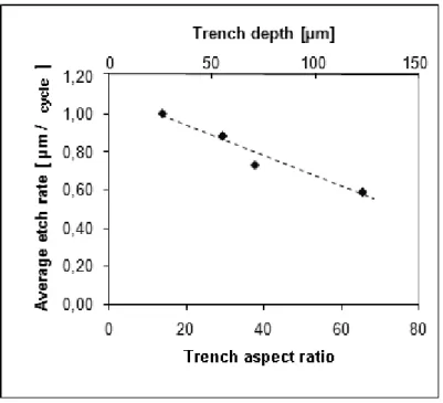
Initial substrate is a (100) single-crystalline silicon wafer. It should be noticed that the crystallographic orientation and resistivity of the silicon substrate are not critical (step 1). As a masking material for Si etching, thermally grown wet oxide and SPR220 photoresist are used. Since a highly selective ICP process is applied for pattern transfer, no additional Cr layer is necessary (step 2). Pattern transfer is completed by a dry etch of SiO2 masking layer in C4F8 + O2 plasma was used for pattern transfer (step 3). In my optimized process no under-etching or sacrificial layer etch is needed, in contrast with Step 3 of the traditional BCT process. In the next step a room temperature Bosch- process is used for deep trench etching (step 4), which is more robust and cheaper than the cryogenic DRIE of the traditional technology. Aspect ratio better than 1:25 can be now achieved using the Bosch-process [4.23]. The surface roughness of the walls, originating from the sequential passivation/etch steps, is approximately 150nm.
26
SiO2 etch Deep Si etch – Bosch process (passivation/etch)
Highly anisotropic
SiO2 etch Isotropic Si etch
Process step Step 3 Step 4 Step 7 Step 8
Pressure 8mtorr 30mtorr / 40mtorr 30mtorr 40mtorr
ICP power 2000W - / 750W - 750W
LF power
(350kHz) - 1W / 8W - 8W
RF power 100W - 200W
C4F8 flow rate 36sccm 100sccm / - -
O2 flow rate 4sccm - -
SF6 flow rate - - / 150sccm - 150sccm
Ar flow rate - - 20sccm
CHF3 flow
rate - - 30sccm
Etch time - 4sec / 9sec (cycle time) 5min 5min
Table 4.1: DRIE etch parameters. A standard cubic centimetre (sccm) is defined as the volumetric flow rate at calibration reference conditions of 1013.25 hPa and 0°C.
As Fig. 4.3 presents, this roughness causes no problems in the following etching steps. After preliminary trench etch a 100nm thick thermal SiO2 is grown on the substrate (step 5), which also removes the residual fluorocarbon-polymers from the passivation step of sidewalls during Bosch-process.
Figure 4.3: Open channels after the isotropic etch of Si.
Electron beam evaporation of a 100nm thick Al layer follows the oxidation (step 6), which will act as a protective coating not only for the planar surfaces, but also for the
27
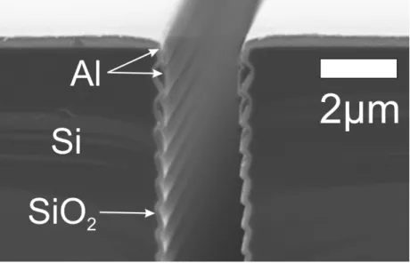
trench edge and the rough sidewall as well (Fig. 4.4). The beneficial effects of the Al layer are detailed later in this chapter.
Figure 4.4: Aluminium step-coverage in the close vicinity of the trench opening
In order to remove the SiO2 protection layer from the bottom of the trench, an anisotropic etch recipe using CHF3 + Ar plasma chemistry is utilized (step 7). The formation of microchannels (isotropic Si etch) is carried out in SF6 plasma (step 8).
During the isotropic Si etch step, the thermally grown 100nm oxide becomes partially free standing, but still mechanically stable. No bending of the material occurred, which could otherwise close the trench and reduce the etch rate. Wet etching of the sidewall protection in BHF for 10 minutes removes both Al and SiO2 protection layers (step 9).
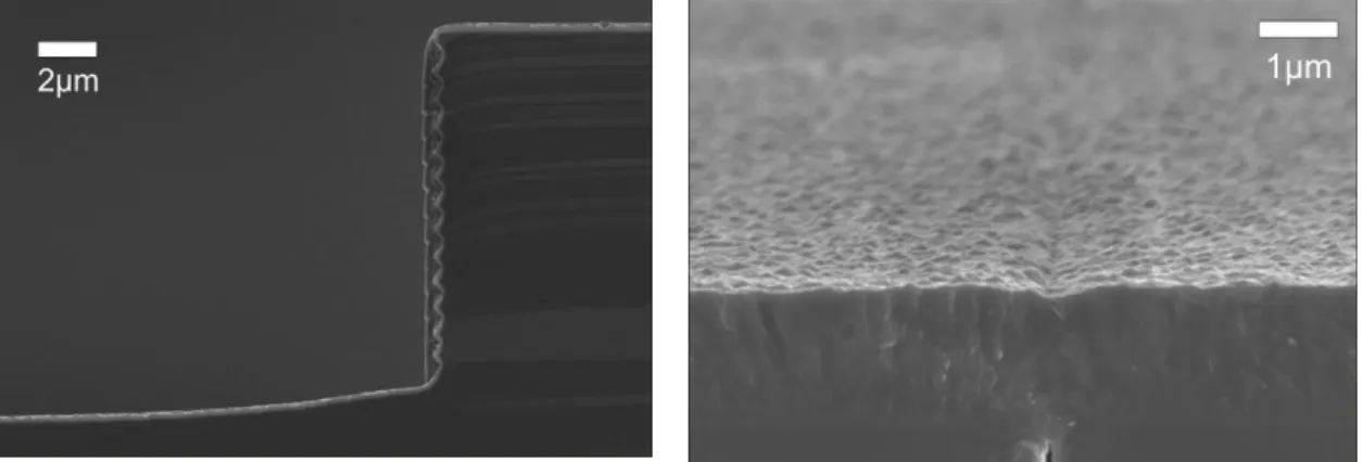
Fig 4.3 shows a cross-sectional image of the channel before filling. After dehydration of the wafers at 300°C, an LPCVD process is applied for closing and sealing of the trenches by poly-Si deposition (step 10). An additional annealing of the poly-Si layer at 1000°C reduces the stress in the deposited layer. A cross section SEM image of a sealed channel is shown on Fig. 4.5.
Figure 4.5: Cross-section of a buried microchannel after the sealing by LPCVD poly-Si deposition is completed.
28
The 100nm thick aluminium masking layer was deposited in order to protect the edges of the trench during both the anisotropic dry SiO2 etching and the isotropic Si etching steps. Since the step-coverage of electron beam evaporation is poor in case of trenches with a small feature size, the bottom of such structures (width close to the micron range) is left almost uncovered, so anisotropic dry oxide etching is not affected significantly [patent pending – 4.24].
The analysis of the step coverage of the evaporation process was carried out using the planetary evaporation model of SILVACO Virtual Wafer Fab [4.24a]. Model parameters were adjusted according to the experimental setup of the Varian 3120 vacuum chamber. Al coverage versus aspect ratio at various trench widths was simulated by the Elite module and is presented by Fig. 4.6.
Figure 4.6: The thickness of Al layer deposited at the bottom of the trench strongly depends on the width (w) and the aspect ratio of that – Al thickness on the plane wafer
surface and at the bottom of the trench is denoted by d0 (100nm) and db respectively.
Images on the step-coverage in the close vicinity of the trench edges are shown on Fig.
4.4.
The Al passivation of the trench edges also modifies the characteristics of the subsequent etching steps. Different masking layers in DRIE processes can influence not only the etch profile but the etch rate as well [4.25-4.26]. Al can easily heat up due to eddy currents, so local rising of temperature might cause increasing etch rate as well as directional changes.
The aspect ratio of the trenches also influences the etch rate. If the aspect ratio is increasing, a thinner Al layer will be present at the bottom of the trench, which affects the anisotropic oxide etch cycle significantly. On the other hand, due to the physical ion depletion and bowing, the effect of diffusion on the supply of reactants to the bottom of the trench, and consumption of reactants at the trench sidewalls is limited [4.25, 4.27], therefore smaller openings are etched slower. These two phenomena are supposed to
29
result in a compensation of aspect ratio dependent etching during the isotropic Si etch (channel formation). The above statements are still being thoroughly investigated in order to determine safety margins of the proposed technology.
The final microstructure after isotropic Si etch of the sample is shown on Fig. 4.5.
Some unique features of the proposed method of edge passivation can be concluded as follows:
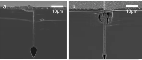
• Due to the step-coverage of e-beam evaporation, trenches, channels or reservoirs of larger feature size (aspect ratio < 5) on the wafer are substantially protected by the aluminium layer from being etched during isotropic Si etch in SF6 plasma (step 8). The effect is apparent on Fig. 4.7. That property enables to form the fluidic inlets simultaneously with the channels using the same lithography step.
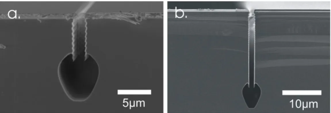
• Further advantage of the proposed edge-protection method is that wafers can be exposed to long Si and SiO2 etch cycles due to the high selectivity of both the anisotropic dry oxide etch and the isotropic dry Si etching [4.28] to the Al + SiO2 masking double-layer. As a result, the formation of microchannels buried deeply below the surface (aspect ratio > 30, at a depth of even 150µm) of the silicon substrate is possible.
• The most apparent benefit of the modified technology is not only the optimized process flow, but the protection of the surface planarity. While under-etching has practically disappeared from the vicinity of the edges, the poor quality of the surface topography above the filled trenches is reduced as well below the micrometer range (see Fig. 4.8). Average depth of the orifices is in the 200-300nm range, while the depth realized by de Boer et al. was approximately 5-10µm.
Figure 4.7: Profile of the isotropic Si etch of a fluidic reservoir (the Si etch is practically inhibited on the surfaces covered by the evaporated aluminium layer).
Figure 4.8: Close SEM view on the surface profile of a sealed trench. It is apparent that the size of the orifice is well below the micron range.
Fig. 4.9 shows a cross-sectional view of a fluidic channel fabricated by the new planar process (a.), and one realized by the traditional technology, while no protection of the coating layers is performed at all (b.). In the first case, the reproducibility and controllability of the process is not reliable. My enhanced process results in a well- controlled, planar poly-Si surface, which enables the further CMOS processing after buried channel formation is complete.
![Figure 2.6: Haemolysis index plotted against shear stress and exposition time [2.17].](https://thumb-eu.123doks.com/thumbv2/9dokorg/1309566.105367/12.892.298.649.592.852/figure-haemolysis-index-plotted-shear-stress-exposition-time.webp)
![Figure 3.6: Bulk micromachined channels [3.16]: (a) glass-glass; (b) silicon-silicon;](https://thumb-eu.123doks.com/thumbv2/9dokorg/1309566.105367/20.892.235.706.104.418/figure-bulk-micromachined-channels-glass-glass-silicon-silicon.webp)