Multilevel Inverter Topology with Modified Pulse Width Modulation and Reduced Switch Count
Thiyagarajan Venkatraman
1, Somasundaram Periasamy
21 Dept. of Electrical and Electronics Engineering, SSN College of Engineering, Chennai, Tamilnadu, India (thiyagarajanv@ssn.edu.in)
2 Dept. of Electrical and Electronics Engineering, Anna University, Chennai, Tamilnadu, India (mpsomasundaram@annauniv.edu)
Abstract: This paper proposes a new inverter topology with minimum switches, which generates a larger numbers of output voltage levels. The major advantages of the presented topology are minimum number of power switches, minimum cost, reduction in installation area and less switching losses. Different algorithms for determination of the magnitude of voltage sources are presented. Digital based switching scheme has been proposed for low switching frequency operation. Comparative analysis of the proposed inverter topology with earlier presented topologies shows that the performance of the proposed topology is improved as compared with conventional and other recently developed topology. The performance of the presented inverter has been analyzed by simulation, using MATLAB and also the feasibility of the topology has been validated experimentally.
Keywords: multilevel inverter; symmetric inverter; asymmetric inverter; total harmonic distortion
1 Introduction
Multilevel inverter (MLI) plays a crucial role in the field of power electronics and widely been employed in high power low voltage applications [1, 2]. It synthesizes a desired staircase output voltage waveform from multiple input DC voltage sources [3]. The DC sources used for MLI may be capacitors, batteries, photovoltaic, wind and fuel cell. Conventional multilevel inverters such as diode- clamped [4, 5], flying capacitor [6, 7] and cascaded H-bridge (CHB) inverters [8, 40] have widely been used over last few decades. Among these topologies, CHB MLI has received more attention because of its simple structure and modularity. It consists of several isolated DC sources and H-bridge units. Based on the magnitude of these isolated DC voltage sources, CHB MLI has been classified as
symmetric and asymmetric [9]. In symmetric type inverter, the magnitudes of DC sources are equal which offers superior modularity, whereas the magnitude of DC voltage sources are not equal in the asymmetric type inverter [10]. It is possible to achieve higher number of output levels during asymmetric operation as compared with symmetric operation for the same amount of switches and DC sources. To achieve large number of output levels, CHB requires increased number of components which increases the complexity and cost. Many researchers proposed new inverter topologies with reduced switch count [9-29]. However, the reduction in the switch count increases the number of sources and power rating of the switching devices [11].
Coupled inductors based 9-level inverter is proposed in [1]. But this topology does not reduces the number of switching components compared to conventional CHB MLI. A generalized topology of the multilevel inverter with coupled inductors is presented in [2]. In order to minimize the size of the inductors, the DC component in the corresponding voltage and current waveforms are eliminated by proper switching strategy. This inverter topology reduces the number of DC sources, however fails to minimize the number of switches. Multicarrier sinusoidal PWM based multilevel inverter is presented in [11]. A fuzzy logic controller [49] based multilevel converter for photovoltaic systems is proposed in [50] This system does not require any optimal PWM switching-angle generator and proportional–integral controller. The cascaded inverter with regeneration capability is proposed in [12].
However, the number of switches is same as CHB MLI. A symmetrical type inverter with reduced switching components is proposed in [13]. In this topology, when the magnitude of DC voltages are not same, it is difficult to achieve all possible output levels. A 5-level inverter topology is presented in [14]. In this, each basic unit consists of conventional H-bridge, one bidirectional switch and two DC sources. In [15], modular current source inverter is presented which operates in both symmetric and asymmetric modes. This topology requires proper current control to achieve all possible output levels. A T-type inverter with modified multiple reference multicarrier based PWM technique is presented in [16]. In [17], a modified modular MLI using series-parallel conversion of DC sources is proposed. This topology requires two independent sources to achieve same number of voltage levels as compared with conventional CHB MLI. A transformer based symmetric and asymmetric type CHB MLI is presented in [18].
In this topology, the peak inverse voltage of the switching devices is reduced considerably. However, the inverter size is bulky because of the presence of transformer. Another topology of multilevel inverter is presented in [19]. This topology reduces the voltage sources and the number of switches compared to CHB MLI. But, it is not possible to achieve all possible levels of output voltage.
Also, this topology needs more number of bidirectional switches for achieving the constant number of output voltage levels. The multilevel inverter topology proposed in [20] operates in both symmetric and asymmetric mode. It also reduces the number of switches to achieve higher output levels. The major drawback of this topology is its complex control algorithm to control the switching operations.
A 4-level inverter is presented in [21]. This topology uses single DC source to achieve the required output levels. The drawback of this inverter topology is it fails to achieve zero level voltage which results in increased switching losses. As compared with the inverter topology presented [36, 48], the proposed topology synthesizes larger number of output levels for the same number of switching components and DC sources.
This paper presents a new inverter topology with a high number of steps associated with a minimum number of power switches. The operation of the proposed inverter topology and different algorithms for the determination of the DC voltage magnitude is presented in Section 2. A brief comparison study is presented in Section 3. The digital based modulation scheme with low switching frequency is explained in Section 4. Simulation results for a symmetrical 9-level and asymmetrical 31-level inverter are presented in Section 5. Section 6 presents the experimental results which show the practicality of the proposed inverter topology and the conclusions are given in Section 7.
2 Proposed Inverter Topology
The proposed structure of the new inverter topology with polarity changing unit is shown in Fig. 1. This topology consists of basic unit and H-bridge unit. The basic unit of the proposed structure is made of two DC voltage sources and four main switches. This inverter topology operates in both symmetric and asymmetric operation.
(a) (b)
Figure 1
Proposed inverter topology (a) Basic unit (b) With H-bridge inverting unit
2.1 Operation
The different operating modes of the proposed inverter is shown in Fig. 2. The switches T1, T2 and T3, T4 helps to reverse the polarity of the output voltage of the basic unit. In this, the switch S4 is used to achieve the zero voltage across the load.
(a) V1 (b) V2
(c) V1 +V2 (b) -V1
(e) -V2 (f) - (V1 +V2)
(g) 0 (During Positive cycle) (h) 0 (During Negative cycle) Figure 2
Different modes of operation
A rectifier unit with an isolation transformer and a capacitor filter forms the DC voltage sources. The proposed inverter can generate five level output during symmetric condition and seven level output during asymmetric condition. The operating modes during symmetric and asymmetric operation of the proposed inverter for obtaining the alternating output voltage across the load are given in Table 1 and Table 2 respectively. It is seen that the switches T1 and T2 were ON during positive cycle of operation while the switches T3and T4 are ON during negative cycle of operation.
Table 1
Switching table for symmetric five level inverter
Output Level ON state switches Voltage
Sources 1 (S3, T1, T2) or (S2, T1, T2) V1 or V2
2 (S1, T1, T2) V1+V2
0 (S4, T1, T2) or (S4, T3, T4) 0
-2 (S1, T3, T4) -(V1+V2)
-1 (S3, T3, T4) or (S2, T3, T4) -V1 or -V2
Table 2
Switching table for asymmetric seven level inverter
Output Level ON state switches Voltage Sources
1 (S3, T1, T2) V1
2 (S2, T1, T2) V2
3 (S1, T1, T2) V1+V2
0 (S4, T1, T2) or (S4, T3, T4) 0
-3 (S1, T3, T4) -(V1+V2)
-2 (S2, T3, T4) -V2
-1 (S3, T3, T4) -V1
2.2 Determination of Voltage Magnitude
To achieve higher number of output levels, the basic unit can be added in series.
The generalized topology of the proposed inverter with an H-bridge inverting unit is shown in Fig. 3. The general structure is made of 'p' number of basic units connected in series. For the simulation analysis, the switches are assumed as ideal and hence, the drop across each switches has been neglected. Therefore, the maximum voltage across the load is synthesized by adding the magnitude of all DC voltage sources and is given by:
p
i i i
o V V
V
1 1 2 (1)
If the magnitude of all DC sources are same i.e.:
p i
where V V
V1i 2i dc 1,2,..., (2)
then the maximum voltage magnitude obtained across the load is given by:
dc
o pV
V 2 (3)
Since each individual basic unit consists of two voltage sources, the relation between the number of voltage sources 'n' and the number of basic units connected in series 'p' is given by:
p
n2 (4)
Figure 3
Generalized inverter topology
The relationship between the number of voltage sources 'n' and the number of levels 'm' during symmetric operation is given by:
2
1
m
n (5)
Similarly, the relationship between the number of voltage sources 'n' and the total number of switches 'Nswitch' during symmetric operation is given by:
2
2
n Nswitch
(6)
From (5) and (6), the relation between 'Nswitch' and 'm' is obtained as:
3
m Nswitch
(7)
It is known that the number of output levels and their corresponding magnitude depends on the magnitude of the different voltage sources. It is also know that the higher output level is achieved during asymmetric operation as compared with symmetric. Therefore, the magnitude of DC sources has to be chosen differently to achieve larger output levels. This paper proposes six algorithms to determine the magnitude of each DC sources. Table 3 shows the comparison of different algorithms of determining the output levels of the proposed inverter.
Table 3
Comparison of the proposed algorithms
Algorithm Magnitude of voltage sources
Number of switches
Maximum Voltage
Number of levels Algorithm - 1
V1,i = V2,i = Vdc where, i = 1, 2, 3. .
.,p
4(p+1) 2pVdc 4p+1
Algorithm - 2 V1,i = V2,i = iVdc
where, i=1, 2, 3. . .,p 4(p+1) p
p1
Vdc 2p2+2p+1 Algorithm - 3 V1,i = V2,i = (2)i-1Vdcwhere, i=1, 2, 3. . .,p 4(p+1) 22p1Vdc 2p+2 - 3 Algorithm - 4 V1,i = V2,i = (3)i-1Vdc
where, i=1, 2, 3. . .,p 4(p+1) 3p1Vdc 2(3p) - 1 Algorithm - 5
V1,i = (2i-1)Vdc
V2,i= (2i)Vdc where, i=1, 2, 3. . .,p
4(p+1) p
2p1
Vdc 4p2+2p+1 Algorithm - 6V1,i = (4)i-1Vdc
V2,i= (2)2i-1Vdc
where, i=1, 2, 3. . .,p
4(p+1)
22p1
Vdc 22p+1 - 1 The number of output voltage levels, magnitude of the DC voltage sources and the maximum obtained voltage across the load are different for each algorithm. The comparison of different algorithms with respect to the number of levels are given in Table 4. The algorithm-1 is corresponding to the symmetric operation of the inverter where the magnitude of all DC voltage sources are same. The remaining algorithms are corresponding to the asymmetric operation of the inverter where each DC voltage sources have different magnitude. It is clear that the maximum magnitude of the output voltage is achieved during asymmetric mode as compared with symmetric mode of operation with same number of DC voltage sources and power switches.Table 4
Comparison of the proposed algorithms for 'm' level
Algorithm Number of basic units
Number of switches
Number of voltage sources Algorithm - 1
4
1
m m3
2
1 m
Algorithm - 2
2 1 1
2 12
m
2 1 1
2 12
m
121
2m 1
Algorithm - 3 log2(m3)2 4
log2(m3)1
2
log2(m3)2
Algorithm - 4 )
2 ( 1
log3 m
1 2 ) ( 1 log
4 3 m
2 ) ( 1 log 2 3 m
Algorithm - 5
4 1 3
4 12
m
4 3
12 3
m
2 1 3
4 12
m
Algorithm - 6
2 1 ) 1 (
log2 m 2
log2(m1)1
log2(m1)1The comparison of the number of voltage sources with the output levels in the different algorithms is shown in Fig. 4(a). Fig. 4(b) shows the comparison of the number of switches with the output levels for the different algorithms.
(a)
(b) Figure 4
Comparison (a)Number of levels vs DC voltage sources (b) Number of levels vs number of switches It is observed that the algorithm-6 requires minimum number of switches and voltage sources to achieve required output levels as compared with other algorithms. However, the drawback of using algorithm-6 is that it requires larger magnitude of DC voltage. It is also observed that the algorithm-5 shows better reduction in the switching devices and the voltage sources during the minimum output levels as compared with algorithm-4. With increase in output level greater than 40, algorithm-4 gives better reduction in the switching components as compared with algorithm-5.
3 Comparison between the Proposed Topology with other Recent Inverter Topologies
In this section, the proposed inverter topology is compared with conventional CHB inverter and other existing multilevel inverter topologies during both symmetrical and asymmetrical modes of operation. Comparison indices used in this paper are number of switching devices, number of DC sources and number of ON-state switches (i.e., conducting switches) required to synthesize any required voltage level. The proposed inverter topology is compared with the symmetrical inverter topologies presented in [13, 22], asymmetrical inverter topologies presented in [19, 23, 24] and other recent topologies which operates in both symmetric and asymmetric mode presented in [11, 15, 20, 25, 36].
3.1 DC Sources
With 'n' DC sources, the proposed inverter achieves 2n+1 levels during symmetric mode which is same as the conventional CHB inverter and other symmetric topologies presented in [11, 15, 20, 23, 25]. It means that this topology achieves 5 level with 2 DC sources, 9 level with 4 DC sources and so on. During asymmetrical modes of operation, the number of levels can vary with respect to the magnitude and number of the DC voltage sources. Fig. 5 shows the comparison of number of levels with the number of DC sources during asymmetrical modes of operation of the proposed inverter topology. It is important to note that the proposed inverter topology achieves higher number of output levels with minimum number of DC voltage sources as compared with topologies presented in [23] and [25].
Figure 5
Levels vs DC sources in asymmetrical mode
3.2 Switches
Fig. 6 shows the comparison of number of levels with the number of switching devices during symmetrical and asymmetrical modes of operation of the proposed inverter topology. It is seen that the proposed inverter topology utilizes minimum number of switching components as compared with conventional CHB, and other topologies presented in [11, 19, 23-25]. For example, to achieve 9-level output voltage during symmetric mode, the proposed topology requires 12 switches which is same as in [25]. Whereas, the conventional CHB and the topology in [11]
requires 16 switches which shows that the number of switching components is reduced by 25%. To achieve 31 level during symmetric operation, the proposed topology requires 34 switches only. However, the required switch count is increased to 60 for CHB and topology presented in [11]. Similarly, the switch
count is increased to 45 for the inverter topology presented in [25] to achieve 31 level during symmetric operation. This shows that the switch count is reduced by 43.33% compared with CHB, [11] and 24.44% compared with [25]. It is also observed that the proposed topology during asymmetrical mode achieves 14.28%
reduction in number of switching components compared with the topology presented in [23], 25% reduction compared with CHB and [24] while synthesizing 31 level output voltage.
(a)
(b) Figure 6
Levels vs switches (a) Symmetrical mode (b) Asymmetrical mode
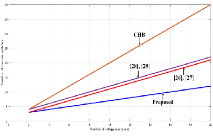
3.3 ON-state Switches
The number of switches in the conduction path is another important parameter to compare the different topologies. The total power loss of the switches depends on the total number of switches in the current conduction path. From Table 1, it is seen that for the proposed inverter topology with single basic unit and H-bridge inverting unit, three switches will be conducting one from the basic unit and two from the H-bridge inverting unit to achieve any desired output levels. The number of on-state switches at any time will depend on the number of basic units connected in series 'p' and is equal to p+2. With 'n' DC voltage sources, the number of switches in the conduction path is 2
2
n whereas for conventional CHB MLI, it is equal to 2n. Fig. 7 shows the comparison of the number of on-state switches against the number of DC voltage sources. It is seen that the on-state switches for the proposed inverter is lower than the conventional CHB inverter and other topologies presented in [26-29]. This will reduces the number of associated gate driver circuits, installation area and overall cost of the proposed inverter topology. Therefore it is concluded that the conduction losses of the proposed topology will be very less as compared with other presented topologies.
Figure 7 On state switches
4 Modified PWM Technique
In MLI, many methods such as pulse width modulation (PWM) [30, 35, 37, 38, 43], selective harmonic elimination (SHE) [31, 41, 52], space vector modulation [32, 42, 44] and active harmonic elimination [33] have been used for modulation control. The PWM governs the consistent conduction of switching devices in the MLI to achieve a preferred output levels. In this paper, a modified multicarrier
based digital PWM technique is used to generate required pulses. In this technique, the generation of the switching signals involves three stages. In stage-1, the reference sinusoidal signal is compared with multiple number of constant amplitude carrier signals to generate the stage-1 signals. The number of carrier signals depends on the number of levels of the inverter and the number of stage-1 signals generated will be equal to the number of carrier signals. For 'm' level inverter, the required number of carrier signals is (m-1)/2. The amplitudes of the different carrier signals are determined using the formula,
2 ..., 1 3 , 2 , 1 1 1 2 max
i m m V i
VCi (8)
where Vmax is the maximum voltage of the reference sinusoidal signal. The stage-2 involves the process of state assignment. In this stage, the state assignment is done for digital values of each generated stage-1 signals during each level of the output voltage. During stage-3, the switching states are obtained against each assigned states. On simplifying the resultant table using reduction techniques, the final switching signals were obtained. During simplification, the unused states are treated as don't cares 'x'. To illustrate this, consider a 9-level symmetrical topology of the proposed inverter. It consists of 4 DC voltage sources and 8 main switches.
Stage-1
For 9-level inverter, four carrier signals were required and these signals were compared with sinusoidal reference signal to generate stage-1 signals C1, C2, C3
and C4 as shown in Fig. 8(a). Since the output voltage waveform is symmetrical, it is enough to consider the signals till π/2. The maximum voltage of the reference sinusoidal signal is 4V and hence, the amplitudes of the carrier signals are determined as 0.5V, 1.5V, 2.5V and 3.5V respectively. The frequency of the reference signal is 50 Hz.
Stage-2
The stage -2 is the process of assigning the states to the stage-1 signals during each interval. The state assignment process is shown in Fig. 8(b). It is important to note that only one bit changes at a time during each state transition. During period 0 to π/2, the state transits from state-1 to state-4 and during period π/2 to π, the state transits from state-4 to state-1.
Stage-3
Table 5 shows the switching conditions of the proposed 9-level inverter for different states. On simplification, the final switching signals were obtained as,
S A S
C B A S C B S
S B A S
22 12
41 31
21 11
0 0
(9)
Table 5
Switching conditions during Stage-3 S.
No States Signals Switches
A B C S11 S21 S31 S41 S12 S22 S32 S42
1 State-0 0 0 0 0 0 0 1 0 0 0 1
2 State-1 0 0 1 0 0 1 0 0 0 0 1
3 State-2 0 1 1 1 0 0 0 0 0 0 1
4 State-3 0 1 0 1 0 0 0 0 0 1 0
5 State-4 1 0 0 1 0 0 0 1 0 0 0
(a)
(b) Figure 8
PWM generation stages (a) Stage-1 (b) Stage-2
5 Simulation Results
To analyze the performance of the proposed inverter topology during the symmetric and asymmetric operation, simulation is carried out. A series connected two basic units with a H-bridge as shown in Fig. 9 is developed using MATLAB/SIMULINK software. The developed model consists of four DC voltage sources and eight main switches. It achieves 9-level during symmetric operation and 31-level during asymmetric operation. A series RL load with magnitudes R= 75 Ω and L = 30 mH are considered as load parameters.
Figure 9
Proposed inverter topology with series connected two basic units
5.1 Symmetric -9-level
During symmetric operation, the magnitude of all DC voltage sources are equal i.e., V11 = V21 = V12 = V22 = Vdc = 60 V. The required PWM signals are generated as explained in section-4 and is shown in Fig. 10.
Figure 10
Switching pulses for 9-level inverter
The output voltage obtained across each basic unit of the proposed inverter topology during the symmetric operation is shown in Fig. 11 and Fig. 12 respectively. During symmetrical operation, the total voltage stress on switches is calculated as 16Vdc.
Figure 11
Output voltage across unit-1 during symmetric operation
Figure 12
Output voltage across unit-2 during symmetric operation
The measured input and output powers are about 440 W and 420 W, respectively with the loss of 20 W. Therefore, the efficiency of the proposed inverter topology during 9-level symmetric operation is about 95.45%. However, the efficiency of the multilevel inverter topology presented in [39] is about 93%. The 9-level output voltage and the corresponding THD are given in Fig. 13. It is observed that the THD of the 9-level output voltage waveform is 10.47% with the fundamental value of the output voltage as 257.6V. The THD comparison of 9-level output voltage waveform for different inverter topologies is given in Table 6. It is observed that the proposed topology achieves minimum THD for the 9-level output voltage waveform.
Table 6
Comparison of THD for 9-level inverter
Topology [29] [45] [46] [11] Proposed
THD (%) 16.20 13.45 12.75 11.41 10.47
(a)
(b) Figure 13
Symmetric 9-Level (a) Output Voltage and (b) THD
5.2 Asymmetric -31-level
During asymmetric operation, the magnitude of all DC voltage sources are different. The magnitude of each DC voltage sources can be determined using algorithm-6 and are given as V11 = Vdc = 16 V, V21 = 2Vdc = 32 V, V12 = 4Vdc = 64 V and V22 = 8Vdc = 128 V. For 31-level inverter, fifteen carrier signals were required and these signals were compared with sinusoidal reference signal to generate fifteen stage-1 signals C1 to C15. The amplitude of these carrier signals were determined using equation (8). The stage-2 signals were determined with an assumption that only one bit changes at a time using the following relation,
15 13 11 9 7 5 3 1
14 12 10 8 6 4 2
12 4 8
C C C C C C C C D
C C C C C C C C
C C B
C A
(10)
On simplification, the switching signals for the 31-level asymmetric inverter were obtained as
B A S D C S
B A S D C S
AB S CD S
B A S D C S
42 32
22 12
41 31
21 11
(11)
The required PWM signals are generated as explained in section-4 and is shown in Fig. 14. The output voltage obtained across each basic unit of the proposed inverter topology during the asymmetric operation is shown in Fig. 15 and Fig. 16 respectively.
Figure 14
Switching pulses for 31-level inverter
Figure 15
Output voltage across unit-1 during asymmetric operation
Figure 16
During asymmetrical operation, the total voltage stress on switches is calculated as 50Vdc. The efficiency of the proposed inverter topology during 31-level asymmetric operation is about 96.32% with the power loss of around 14.85 W.
The 31-level output voltage and the corresponding THD are given in Fig. 17. It is observed that the THD of the 31-level output voltage waveform is 2.70% with the fundamental value of the output voltage as 246.3 V.
(a)
(b) Figure 17
Asymmetric 31-Level (a) Output Voltage and (b) THD
The THD comparison of 31-level output voltage waveform for different inverter topologies is given in Table 7. It is observed that the proposed topology achieves minimum THD for the 31-level output voltage waveform. Fig. 18 shows the %THD value for different modulation indices during symmetrical and asymmetrical operation of the proposed inverter. From the graph, it is clearly shown that %THD decreases with increase in the modulation index and it is also shown that %THD for the proposed inverter topology during the asymmetric operation is lesser that of symmetric operation for the same modulation index.
Table 7
Comparison of THD for 31-level inverter
Topology [46] [26] [34] Proposed
THD (%) 4.66 4.04 3.26 2.70
Figure 18
%THD for different modulation indices
6 Hardware Results
To show the feasibility of the proposed inverter topology, a hardware setup of 9- level symmetrical topology is considered. The experimental setup consists of two basic blocks connected in series with each block consists of two DC sources with equal magnitude as 16V. A rectifier unit with an isolation transformer and a capacitor filter forms the DC voltage sources. The diode IN4007 acts as a bridge rectifier unit. To get the constant voltage to the controller, IC7805 acts as a voltage regulator. The gate signals for driving the power switches has been generated with the help of 16-bit digital signal controller dsPIC30F2010. As seen from Table 5, the switches S21 and S22 were neglected and therefore 10 MOSFET (IRF840N) power switches were employed in the hardware setup. Fig. 19 shows the experimental results for the symmetric 9-level inverter. It is observed that the THD of the 9-level output waveform is achieved as 11%.
(a)
(b) Figure 19
Hardware results (a) 9-level Output Voltage and (b) THD
Conclusions
In this paper, a new topology of a symmetrical and asymmetrical type, multilevel inverter, with reduced switch count, is proposed. Different algorithms for the determination of the magnitude of the DC voltage sources are analyzed. The comparative analysis of the proposed inverter topology with other recent topologies show that the proposed topology significantly reduces the number of DC voltage sources and power switches. The advantages of the proposed topology include simple construction, ease of control, a reduced number of components, lower THD and a minimized cost. The number of on-state switches in the conduction path, are also reduced, as compared with other existing topologies. The performance of the proposed inverter topology is analyzed for 9-level symmetrical and 31-level asymmetrical cases. Finally, the feasibility of the proposed inverter
topology for 9-level symmetrical operation has been tested experimentally. The experimental results are in good agreement with the simulation results.
Acknowledgements
This research work was supported and funded by SSN Trust.
References
[1] S. H. Ashan and M. Monfared: Design and comparison of nine-level single- phase inverters with a pair of coupled inductors and two dc sources, IET Power Electronics, Vol. 9, No. 11, pp. 2271-2281, 2016
[2] S. H. Ashan and M. Monfared: Generalised single-phase N-level voltage- source inverter with coupled inductors, IET Power Electronics, Vol. 8, No.
11, pp. 2257-2264, 2015
[3] E. Zamiri, N. Vosoughi, S. H. Hosseini, R. Barzegarkhoo and M. Sabahi: A New Cascaded Switched-Capacitor Multilevel Inverter Based on Improved Series–Parallel Conversion With Less Number of Components, IEEE Transactions on Industrial Electronics, Vol. 63, No. 6, pp. 3582-3594, 2016 [4] A. Nabae, I. Takahashi and H. Akagi: A New Neutral-Point-Clamped PWM Inverter, IEEE Transactions on Industry Applications, Vol. IA-17, No. 5, pp. 518-523, 1981
[5] J. Rodriguez, S. Bernet, P. K. Steimer and I. E. Lizama: A Survey on Neutral-Point-Clamped Inverters, IEEE Transactions on Industrial Electronics, Vol. 57, No. 7, pp. 2219-2230, 2010
[6] C. Feng, J. Liang and V. G. Agelidis: Modified Phase-Shifted PWM Control for Flying Capacitor Multilevel Converters, IEEE Transactions on Power Electronics, Vol. 22, No. 1, pp. 178-185, 2007
[7] T. A. Meynard, H. Foch, F. Forest, C. Turpin, F.Richardeau, L.Delmas, G.
Gateau and E. Lefeuvre: Multicell converters: derived topologies, IEEE Transactions on Industrial Electronics, Vol. 49, No. 5, pp. 978-987, 2002 [8] F. Z. Peng and J. S. Lai: Multilevel cascade voltage source inverter with
separate DC sources, U.S. Patent 5 642 275, 1997
[9] K. K. Gupta, A. Ranjan, P. Bhatnagar, L. K. Sahu and S. Jain: Multilevel Inverter Topologies With Reduced Device Count: A Review, IEEE Transactions on Power Electronics, Vol. 31, No. 1, pp. 135-151, 2016 [10] S. P. Gautam, L. Kumar and S. Gupta: Hybrid topology of symmetrical
multilevel inverter using less number of devices, IET Power Electronics, Vol. 8, No. 11, pp. 2125-2135, 2015
[11] K. K. Gupta and S. Jain: Topology for multilevel inverters to attain maximum number of levels from given DC sources, IET Power Electronics, Vol. 5, No. 4, pp. 435-446, 2012
[12] P. Lezana, J. Rodriguez and D. A. Oyarzun: Cascaded Multilevel Inverter With Regeneration Capability and Reduced Number of Switches, IEEE Transactions on Industrial Electronics, Vol. 55, No. 3, pp. 1059-1066, 2008 [13] M. F. Kangarlu, E. Babaei and S. Laali: Symmetric multilevel inverter with reduced components based on non-insulated dc voltage sources, IET Power Electronics, Vol. 5, No. 5, pp. 571-581, 2012
[14] C. I. Odeh and D. B. N. Nnadi: Single-phase 9-level hybridised cascaded multilevel inverter, IET Power Electronics, Vol. 6, No. 3, pp. 468-477, 2013
[15] E. S. Najmi and A. Ajami: Modular symmetric and asymmetric reduced count switch multilevel current source inverter, IET Power Electronics, Vol. 9, No. 1, pp. 51-61, 2016
[16] H. P. Vemuganti, D. Sreenivasarao and G. Siva Kumar: Improved pulse- width modulation scheme for T-type multilevel inverter, IET Power Electronics, Vol. 10, No. 8, pp. 968-976, 2017
[17] M. Kaliamoorthy, V. Rajasekaran, I. G. Christopher Raj and L. Hubert Tony Raj: Generalised hybrid switching topology for a single-phase modular multilevel inverter, IET Power Electronics, Vol. 7, No. 10, pp.
2472-2485, 2014
[18] A. Farakhor, R. R. Ahrabi, H. Ardi and S. N. Ravadanegh: Symmetric and asymmetric transformer based cascaded multilevel inverter with minimum number of components, IET Power Electronics, Vol. 8, No. 6, pp. 1052- 1060, 2015
[19] E. Babaei, S. H. Hosseini, G. B. Gharehpetian, M. T. Haque, M. Sabahi:
Reduction of dc voltage sources and switches in asymmetrical multilevel converters using a novel topology, Electric Power Systems Research, Vol.
77, pp. 1073-1085, 2007
[20] A. Mokhberdoran and A. Ajami: Symmetric and Asymmetric Design and Implementation of New Cascaded Multilevel Inverter Topology, IEEE Transactions on Power Electronics, Vol. 29, No. 12, pp. 6712-6724, 2014 [21] G. S. Perantzakis, F. H. Xepapas and S. N. Manias: A Novel Four-Level
Voltage Source Inverter—Influence of Switching Strategies on the Distribution of Power Losses, IEEE Transactions on Power Electronics, Vol. 22, No. 1, pp. 149-159, 2007
[22] M. R. J. Oskuee, E. Salary and S. N. Ravadanegh: Creative design of symmetric multilevel converter to enhance the circuit's performance, IET Power Electronics, Vol. 8, No. 1, pp. 96-102, 2015
[23] M. Jayabalan, B. Jeevarathinam and T. Sandirasegarane: Reduced switch count pulse width modulated multilevel inverter, IET Power Electronics, Vol. 10, No. 1, pp. 10-17, 2017
[24] E. Babaei: A Cascade Multilevel Converter Topology With Reduced Number of Switches, IEEE Transactions on Power Electronics, Vol. 23, No. 6, pp. 2657-2664, 2008
[25] E. Babaei, S. Laali and S. Alilu: Cascaded Multilevel Inverter With Series Connection of Novel H-Bridge Basic Units, IEEE Transactions on Industrial Electronics, Vol. 61, No. 12, pp. 6664-6671, 2014
[26] M. R. Banaei, M. R. J. Oskuee and H. Khounjahan: Reconfiguration of semi-cascaded multilevel inverter to improve systems performance parameters, IET Power Electronics, Vol. 7, No. 5, pp. 1106-1112, 2014 [27] M. R. Banaei and E. Salary: Verification of New Family for Cascade
Multilevel Inverters with Reduction of Components, Journal of Electrical Engineering and Technology, Vol. 6, No. 2, pp. 245-254, 2011
[28] E. Babaei, S. H. Hosseini: New cascaded multilevel inverter topology with minimum number of switches, Energy Conversion and Management, Vol.
50, pp. 2761-2767, 2009
[29] A. Ajami, M. R. J. Oskuee, A. Mokhberdoran and A. Van den Bossche:
Developed cascaded multilevel inverter topology to minimise the number of circuit devices and voltage stresses of switches, IET Power Electronics, Vol. 7, No. 2, pp. 459-466, 2014
[30] B. P. McGrath and D. G. Holmes: Multicarrier PWM strategies for multilevel inverters, IEEE Transactions on Industrial Electronics, Vol. 49, No. 4, pp. 858-867, 2002
[31] H. Lou, C. Mao, D. Wang, J. Lu and L. Wang: Fundamental modulation strategy with selective harmonic elimination for multilevel inverters, IET Power Electronics, Vol. 7, No. 8, pp. 2173-2181, 2014
[32] O. Lopez, J. Alvarez, J. D. Gandoy and F. D. Freijedo: Multilevel Multiphase Space Vector PWM Algorithm, IEEE Transactions on Industrial Electronics, Vol. 55, No. 5, pp. 1933-1942, 2008
[33] Z. Du, L. M. Tolbert and J. N. Chiasson: Active harmonic elimination for multilevel converters, IEEE Transactions on Power Electronics, Vol. 21, No. 2, pp. 459-469, 2006
[34] R. S. Alishah, S. H. Hosseini, E. Babaei and M. Sabahi: Optimal Design of New Cascaded Switch-Ladder Multilevel Inverter Structure, IEEE Transactions on Industrial Electronics, Vol. 64, No. 3, pp. 2072-2080, 2017 [35] S. F. Ahmed, C. F. Azim, H. Desa and A. S. T. Hussain: Model Predictive Controller-based, Single Phase Pulse Width Modulation (PWM) Inverter for UPS Systems, Acta Polytechnica Hungarica, Vol. 11, No. 6, pp. 23-38, 2014
[36] V. Thiyagarajan and P. Somasundaram: Modeling and Analysis of Novel
Components, CMES: Computer Modeling in Engineering and Sciences, Vol. 113, No. 4, pp. 461-473, 2017
[37] I. Vajda, Y. N. Dementyev, K. N. Negodin, N. V. Kojain, L. S. Udut, I. А.
Chesnokova: Limiting Static and Dynamic Characteristics of an Induction Motor under Frequency Vector Control, Acta Polytechnica Hungarica, Vol.
14, No. 6, pp.7-27, 2017
[38] V. Thiyagarajan and P. Somasundaram: Analysis of Multicarrier PWM techniques for Photovoltaic fed Cascaded H-Bridge Multilevel Inverter, Journal of Electrical and Electronics Engineering, Vol. 10, No. 1, pp. 85- 90, 2017
[39] K. Boora and J. Kumar: General topology for asymmetrical multilevel inverter with reduced number of switches, IET Power Electronics, Vol. 10, No. 15, pp. 2034-2041, 2017
[40] M. Saeedian, J. Adabi and S. M. Hosseini: Cascaded multilevel inverter based on symmetric–asymmetric DC sources with reduced number of components, IET Power Electronics, Vol. 10, No. 12, pp. 1468-1478, 2017 [41] P. L. Kamani and M. A. Mulla: Middle-Level SHE Pulse-Amplitude Modulation for Cascaded Multilevel Inverters, IEEE Transactions on Industrial Electronics, Vol. 65, No. 3, pp. 2828-2833, 2018
[42] B. Kirankumar, Y. V. Siva Reddy and M. Vijayakumar: Multilevel inverter with space vector modulation: intelligence direct torque control of induction motor, IET Power Electronics, Vol. 10, No. 10, pp. 1129-1137, 2017
[43] S. K. Sahoo and T. Bhattacharya: Phase-Shifted Carrier-Based Synchronized Sinusoidal PWM Techniques for a Cascaded H-Bridge Multilevel Inverter, IEEE Transactions on Power Electronics, Vol. 33, No.
1, pp. 513-524, 2018
[44] J. S. Hu, J. N. Lin and H. C. Chen: A Discontinuous Space Vector PWM Algorithm in abc Reference Frame for Multilevel Three-Phase Cascaded H- Bridge Voltage Source Inverters, IEEE Transactions on Industrial Electronics, Vol. 64, No. 11, pp. 8406-8414, 2017
[45] N. Arun and M. M. Noel: Crisscross switched multilevel inverter using cascaded semi-half-bridge cells, IET Power Electronics, Vol. 11, No. 1, pp.
23-32, 2018
[46] A. Ajami, M. R. J. Oskuee, M. T. Khosroshahi and A. Mokhberdoran:
Cascade-multi-cell multilevel converter with reduced number of switches, IET Power Electronics, Vol. 7, No. 3, pp. 552-558, 2014
[47] F. Chabni, R. Taleb and M. Helaimi: ANN-based SHEPWM using a harmony search on a new multilevel inverter topology, Turkish Journal of
Electrical Engineering and Computer Sciences, Vol. 25, No. 6, pp. 4867- 4879, 2017
[48] M. Ramya and P. Usha Rani: Asymmetrical Cascaded Twenty Seven level Inverter based STATCOM, Rev. Roum. Sci. Techn.–Électrotechn.
etÉnerg., Vol. 62, No. 4, pp. 411-416, 2017
[49] R. E. Precup, S. Preitl and P. Korondi: Fuzzy Controllers With Maximum Sensitivity for Servosystems, IEEE Transactions on Industrial Electronics, Vol. 54, No. 3, pp. 1298-1310, 2007
[50] C. Cecati, F. Ciancetta and P. Siano: A Multilevel Inverter for Photovoltaic Systems With Fuzzy Logic Control, IEEE Transactions on Industrial Electronics, Vol. 57, No. 12, pp. 4115-4125, 2010
[51] V. Thiyagarajan and P. Somasundaram: Modified Seven Level Symmetric Inverter with Reduced Switch Count, Advances in Natural and Applied Sciences, Vol. 11, No. 7, pp. 264-271, 2017
[52] F. Chabni, R. Taleb, M. Helaimi: Output voltage waveform improvement of modified cascaded H-bridge multilevel inverter using selective harmonic elimination technique based on hybrid genetic algorithm, Rev. Roum. Sci.
Techn.–Électrotechn. etÉnerg., Vol. 62, No. 4, pp. 405-410, 2017