New Resonant Inverter Tuning for Three-Phase Current Source Parallel Resonant Inverters
Alireza Namadmalan
1, Javad Shokrollahi Moghani
21Jundi-Shapur University of Technology, Dezful, Iran, namadmalan@jsu.ac.ir
2Amirkabir University of Technology, Tehran, Iran, moghani@aut.ac.ir
Abstract: This paper presents a new tuningloop for three-phase current source parallel resonant inverters. The switching frequency is tuned by using a phase-locked loop (PLL) circuit based on a new Phase Detector (PD). In practice, the resonant capacitors and inductors have tolerances that cause different resonant frequency for each phase. This paper shows that a conventional PDcauseshigher voltage stress over switches and DC-link inductor. In the proposed tuning loop, the PLL tracks the average value of the resonant frequencies that reduces the voltage stress. In addition, there is no feedback from the loadcurrents to detect the phase error, which is another advantage of the new method. A laboratory prototype of a three-phase current source parallel resonant half-bridge inverter was built to verify the advantages of the proposed tuning system with operating frequency of 22 kHz.
Keywords: resonant inverter tuning; three-phase current source parallel resonant inverters; phase-locked loop (PLL)
1 Introduction
Resonant Inverters are most commonly used because they provide sinusoidal waveforms with lower harmonics and less EMI problems. A large number of topologies have been developed in this area which can be divided into single- phase and multi-phase structures. Three-phase resonant inverters are widely used in industrial applications. Such applications include high power DC-DC converters, contact-less power transfer systems and multi-phase induction heating systems [1-13].
In comparison with single-phase resonant inverters, the three-phase inverters have a smaller input filter and higher power density. Moreover, the load currents and output voltages have less distortion due to third order harmonics elimination for three-wire structures. Hence, the three-phase resonant inverters have better sinusoidal waveforms in low quality factors (Q<5) which is important in traveling wave induction heating systems [9].
Three-phase current-fed parallel resonant inverters are widely utilized in high voltage and high power DC-DC converters; because they provide higher boosting ratio and they have no current sharing problems. The current source inverters have limited control methods but they are less affected by input voltage ripples and they have short-circuited protection capability [13-20]. Figure 1 shows two possible topologies for three-phase current source parallel resonant inverters with three- wire connection.
Conventionally, PDs measure the phase difference between the voltage and the current of a single resonant tank [21-25]. Hence, a conventional PLL is applicable when the three resonant tanks have a same resonant frequency. However, designing the three resonant tanks without tolerance and frequency deviation is practically impossible. This paper shows that the three-phase current source topologies are sensitive to the tolerances and the systems are unbalanced under no-load and light-load conditions. In addition, the switching losses, DC-link current ripples and voltage stress are increased. The proposed PD tracks the average value of the resonant frequencies that reduces the DC-link current ripples and voltage stress over the switches S1-S6.
In a conventional tuning loop, the current of resonant tank is measured for phase error detection. In the new PLL, voltages of the low-side switches are the inputs of the PD and there is no feedback from the output currents. Thus, there is no Current Transformer (CT) or Hall Effect sensor for current sensing, which makes the system simple, more reliable and cost effective. The dynamic behavior of the new tuning loop is simulated in steady state and transient conditions. The proposed PD has similar structure for the two topologies, as shown in Figure 1. For simplicity, the laboratory prototype is implemented based on the half-bridge inverter.
Load
(b) (a)
L1 L2 L3
Ld
S2 S3
S1
S1
S2 S4
S3 S5
S6
Vin Vin Load
Figure 1
Three-phase current source parallel resonant topologies: (a) the full-bridge inverter; (b) the half-bridge inverter
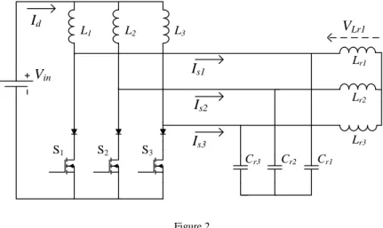
2 System Description
Figure 2 shows the half-bridge topology with a star-connected resonant tank. The performance of the resonant inverter tuning is similar for the half-bridge and full- bridge inverters. In the both cases, each switch conducts 120 degrees to achieve Zero Voltage and Zero Current Switching (ZVZCS) at the resonant frequency.
The half-bridge inverter has asymmetrical current injection while the full-bridge inverter has symmetrical current injection.
Lr1
Vin
L1 L2 L3
Lr3
Lr2
VLr1
Cr3 Cr2 Cr1
Id
Is3
Is1
Is2
S2 S3
S1
Figure 2
The half-bridge inverter with star-connected resonant tank
Figure 3 shows the three-step operation of the half-bridge inverter where each switch conducts for 120 degrees of the switching period. Each switch is connected in series with a blocking diode to prevent the internal body diode of the switches from short circuit. Operation of the inverters is investigated with and without the tolerances as follows:
S2 S3 S1
S2 S3 S1
(a) (b) (c)
S2 S3 S1
Figure 3
Three-step operation of the half bridge inverter
2.1 Operation without the Tolerances
In this section, the parameters of the inverter are considered with no tolerance.
Hence, the three resonant tanks have a similar resonant frequency. The inductance of L1, L2 and L3 (Ld for full-bridge inverter as seen from Figure 1) are much larger than the resonant inductors (Lr1 = Lr2 = Lr3 = Lr), so under normal steady state operation the DC-link current, Id, is approximately constant.
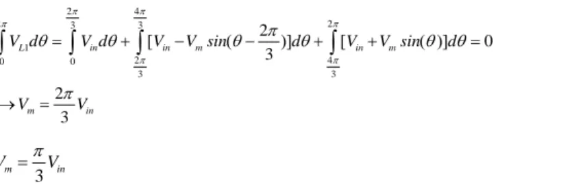
Regarding Figure 3, voltage of S1 is derived by equation (1) for a switching period duration while the converter works at the resonant frequency. The ωr, Ts, Cr and Vm are the angular resonant frequency, switching period, per-phase resonant capacitor and phase-phase voltage of the inverter.
1
1
1
0 0
3
2 2 1
3 3 3 2
2 3
s S
s s
S m r r r
r r s
S m r s
V , t T
T T
V V sin t , t , f
L C
V V sin t , T t T
(1)
For the half-bridge inverters, the amplitude of the phase-phase voltage, Vm, is derived by employing the inductor volt-second balance principle on L1, where Vin is the DC-link voltage. Similarly, Vm is derived by equation (3) for the full-bridge inverters by employing the inductor volt-second balance principle on Ld.
2 4
2 3 3 2
1
2 4
0 0
3 3
2 0
3 2
3
L in in m in m
m in
V d V d V V sin d V V sin d
V V
(2)m 3 in
V V (3)
Figure 4 shows per-phase equivalent circuit of the resonant inverter and R is the per-phase load resistance. According to 1200 conduction, the Is1 and voltage of S1 are shown in Figure 5 for the full-bridge and half bridge topologies at the resonant frequency. For the both topologies, the peak voltage of the switches is the amplitude of the phase-phase voltage or Vm. The DC-link voltage, Vin, of the two topologies is 50 V. As seen from Figure 5(b), the injected current of the full- bridge inverter has no third order harmonics. Hence, the inverter have lower THD of current for low quality factor operations (Q<5), in comparison with single- phase topologies [14-20].
The quality factor of the parallel resonant load is derived by equation (4). For the half-bridge topology, the injected current has second order harmonics and is suitable for high quality factor operations. In addition, the half-bridge topology is useful for high boosting ratio converters, as shown in equation (2).
r r
Q R
L
(4)
R Cr Lr
I
sFigure 4
Single-phase equivalent circuit of the resonant tank and the inverter
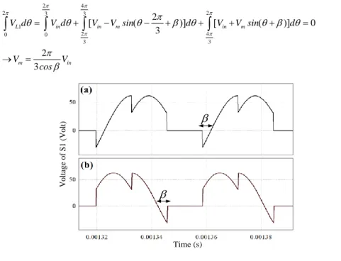
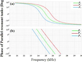
Let’s consider that the switching frequency of the inverter is greater (or smaller) than the resonant frequency. Hence, there is a phase difference, β, between the injected current, Is, and voltage of the tank circuit. Figure 6 shows the phase plot of a parallel resonant tank with quality factor of10 and resonant frequency of 25 kHz. The phase plot represents the phase difference β between the injected current Is and the resonant tank voltage for different switching frequencies.
Figure 5
The voltage of S1 and the injected current connected to S1, Is1: (a) for the half-bridge inverter;
(b) voltage for the full-bridge inverter
Figure 6
Phase plot of a parallel resonant tank with quality factor of 10
Figure 7 shows the voltage of S1 and the phase difference β for two conditions (over and under the resonant frequency). Regarding equation (2), the peak value of the phase-phase voltage, Vm, is rewritten as follows:
2 4
2 3 3 2
1
2 4
0 0
3 3
2 0
3 2
3
L in in m in m
m in
V d V d V V sin d V V sin d
V V
cos
(5)
Time (s)
Voltage of S1 (Volt)
Figure 7
Voltage of S1 at the two different conditions: (a) over the resonant frequency; (b) under the resonant frequency
Forthe full-bridge topology, the equation (5) is rewritten as follows:
m 3 in
V V
cos
2.2 Operation with the Tolerances
Let’s consider that each resonant tank has different parameters (different Lr and Cr). Hence, the frequency deviation Δf caused by the tolerances is derived as follows:
1 4 2
r r r r r r r
r r
r r r r r r r r
f f L C f L C
f L C f
L C L C L C L C
(6)
Figure 8(a) and Figure 8(b) show the phase plot of the three parallel resonant tanks with quality factors of 10 and 2, respectively. The frequency deviations for the resonant tanks1 to 3 are assumed to be 0%, +3% and -3%, respectively. The average value of the three resonant frequencies (fr1, fr2 and fr3) is 25 kHz.
Figure 8
The phase plot of three parallel resonant tanks: (a) quality factor of 10; (b) quality factor of 2 According to equation (2), the phase-phase voltages of the resonant tanks are derived by solving the equations (7) through (9):
2 4
2 3 3 2
1 2 2 3 3
2 4
0 0
3 3
2 0
L in in m 3 in m
V d V d V V sin d V V sin d
(7)2 4
2 3 3 2
2 3 3 1 1
2 4
0 0
3 3
2 0
L in in m 3 in m
V d V d V V sin d V V sin( d
(8)2 4
2 3 3 2
3 1 1 2 2
2 4
0 0
3 3
2 0
L in in m 3 in m
V d V d V V sin d V V sin d
(9)2 2 3 3
3 3 1 1
1 1 2 2
2
6 6 3
2
6 6 3
2
6 6 3
m m in
m m in
m m in
V cos V cos V
V cos V cos V
V cos V cos V
(10)
TheVL1, VL2andVL3are voltage of the DC-link inductors (L1, L2 and L3). According to Figure 2, the Vm1, Vm2 and Vm3are equal to the following values:
1 1 2
2 2 3
3 3 1
m Lr Lr
m Lr Lr
m Lr Lr
V V V
V V V
V V V
(11)
VLr1, VLr2 and VLr3 are the voltage ofthe resonant inductors shown in Figure 2. By solving the equation set (10), the phase-phase voltages are derived as a function of β1, β2, β3 and Vin. For the full-bridge inverter, the equation set (10) can be rewritten by employing the inductor volt-second balance principle onLdand considering the following complex equation:
1 1 2 2 3 3
2 2
0 1
3 3
m m m
V exp j V exp j j V exp j j , j (12) Figure 9 shows the phase-phase voltages of the full-bridge inverter with frequency deviations. In this figure, the resonant frequencies, fr1, fr2 and fr3 are 25 kHz, 26.5 kHz and 25 kHz, respectively (+6% deviations for fr2). The quality factor of each resonant tank is approximately 20 and the DC-link voltage, Vin, is 50 V. In Figure 9(a), a conventional PLL tracks the resonant frequency of fr2 at steady state condition, hence the switching frequency is 26.5 kHz.
Figure 9
Phase-phase voltage of full bridge parallel resonant inverter: (a) the switching frequency is 26.5 kHz;
(b) the switching frequency is 25.5 kHz
Figure 9(b) shows the phase-phase voltages of the full-bridge inverter with the same tolerances. In Figure 9(b), the PLL tracks the average value of the three resonant frequencies, 25.5 kHz, by using the proposed PLL.
Comparing Figure 9(a) and Figure 9(b), it can be concluded that the voltage stress of the inverter is reduced by 20% when the switching frequency is equal to the average value of the resonant frequencies, 25.5 kHz. Hence, for high quality factor (or light-load) conditions (Q>5), the voltage stress of the inverter is significant when the resonant inverter tuning is based on single-phase tuning or conventional PD’s.
It can be proven that the minimum value of the voltage stresses occurs when the equation (13) is satisfied. The equation (13) shows a condition that the switching frequency is set to the average value of the resonant frequencies. In the next section, this condition and the performance of the proposed PLL are described in more details.
1 2 3 1 2 3 0
m m m
min max V ,V ,V (13)
Without loss of generality, consider that the switching frequency of the inverter is tuned by using a conventional PLL that tracks the resonant frequency of fr1. Regarding equations (10) through (13), there is extra voltage stress. The extra stress is maximum for nonsymmetrical tolerances (e.g. ±0 %, ±0 % and ±6 %), and is minimum for symmetrical tolerances (e.g. +3%, -3% and ±0%). The voltage stress increases the current ripples of the DC-link inductor and decreases the net efficiency. The extra voltage stress is suppressed by using the proposed method, which satisfies the equation (13).
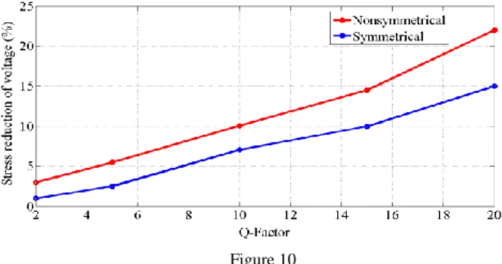
Figure 10 shows the stress reduction (in percentage) of the proposed technique for different quality factors and for nonsymmetrical and symmetrical tolerances.
Figure 11 shows the voltage of the DC-link inductorwhen the full-bridge inverter is tuned by the conventional and proposed methods at quality factor of about 10 and nonsymmetrical tolerances. Regarding Figure 10 and Figure 11, the DC-link ripples are more affected by the voltage stress for a specific quality factor and frequency deviation.
Figure 10
Percentage of stress reduction for the symmetrical and nonsymmetrical tolerances
Figure 11
Voltage of DC-link inductor for the proposed and conventional techniques at quality factor of 10 for the full-bridge topology
Forlow quality factors, the system approximately works like a balanced three- phase system because the phase deviations are negligible, see Figure 8(b) and equation set (10). However, the switching frequency should be equal to the average value of the resonant frequencies to minimize the switching losses, negative sequences and DC-link current ripples.
3 The Proposed Resonant Inverter Tuning
PLL circuit consists of a Voltage Controlled Oscillator (VCO), Phase Detector (PD) and a Loop Filter (LF). There are three important parameters for a PLL circuit: VCO’s gain KV, center frequency fc and LF parameters [25]. In this paper, the LFs are RC filterswith time constant of τ.
A three-phase PD is proposed which only uses the voltage of the switches and has no current sensor in the tuning loop. The PD directly connects to LF units to build a Multiplier PD mode [23-25]. To construct the three-phase PD, voltages of S1, S2, and S3 (VS1, VS2 and VS3) are passed through comparators and then connected to a logic circuit to produce the phase error signals. According to comparators, the voltage of the switches are saturated in both positive and negative values to produce VS1+, VS1-, VS2+, VS2-, VS3+ and VS3-. Figure 12(a) shows waveforms of VS1, VS1-and VS1+ when the inverter works at over the resonant frequency. Figure 12(b) and 12(c) show the voltage of the switches at over and under the resonant frequency for thehalf-bridge inverter and input voltage of 25 V.
Regarding Figure 12, the phase differences (β1, β2 and β3) aresimplyproduced by using AND gates. For instance, to produce the β1 when the inverter works at over the resonant frequency (or β1< 0),VS1- and VS3+ are the inputs of the AND gate, see Figure 12(b).
3
20 Volt/Div
20 µSec/Div
2
1 1
2
3
Figure 12
Switches’ voltages: (a) voltage of S1 and its positive and negative duration; (b) voltage of switches at over the resonant frequency; (c) voltage of switches at under the resonant frequency Equation (14) shows the relationships between β1 and voltage of the switches. The output of the AND gates are passed through Loop Filters (LF) to remove high frequency components.
1 1 3 1 1
1 1 3 1
1 2 1
2 1 2 1
2 1 2 1 1
0
0 0
0 0
0
S S
S S
S S
S S
x V &V ,
x V &V ,
x x
x V &V ,
x V &V ,
(14)
To produce the three-phase PD signals, there are six AND signals,x1… x6, which are implemented to produce the phase differences as follows:
1 1 3 2 1 2 1
3 2 1 4 2 3 2
5 3 2 6 3 1 3
S S S S
S S S S
S S S S
x V &V , x V &V for x V &V , x V &V for x V &V , x V &V for
(15)
According to (15) and Figure 12, the output of phase detector, α is derived as follows:
1 2 3 x2 x4 x6 x1 x3 x5
(16) Figure 13 shows the proposed PD circuit with VCO and LF units. To analyze the performance of the PLL, the phase plot of thetank circuits must be linearized at their resonant frequencies as follows [21-23].
2
ri i
i f f
j f
K |
f
(17)
The Kβ1, Kβ2 and Kβ3 are the slope of the phase curves near their resonant frequencies in rad/Hz. According to Figure 8 and considering that the deviations are below 3%, theslopes are similar for |βi|<300.
buffer
buffer
+- LF
LF
1
+
3f /s 6fs VCO
…
…
2
3
x1
x2
VS1-
VS3+
PI VS1-
VS2+
Figure 13
The proposed three-phase PD with VCO and LF units
1 2 3
K K K K
Therefore, the phase differencescan be derived by equation (18) as follows:
1 1
2 2
3 3
r s
r s
r s
K f f
K f f
K f f
(18)
The fs is the switching frequency of the inverter. Hence, the equation (16) is rewritten as follows:
1 2 3 3
r r r s
K f f f K f
(19)
At steady state condition, α isapproximately zero and hence, the switching frequency is derived as follows:
1 2 3
0 3
r r r
s
f f f
f (20)
By designing a proper PI controller, αis close to zero at steady state condition.
According to (20), the proposed PLL tracks the average value of the resonant frequencies. As seen from Figure 14, the output of the PD is passed through the PI controller. The output of the controller is connected to the VCO unit. According to Figure 12 and equation (16), it is worth noting that the high frequency component of the proposed PD is six times the switching frequency (or three times the conventional PD’s) [21-25]. Therefore, the proposed method has fast dynamics and the tuning process occurs in less cycles.
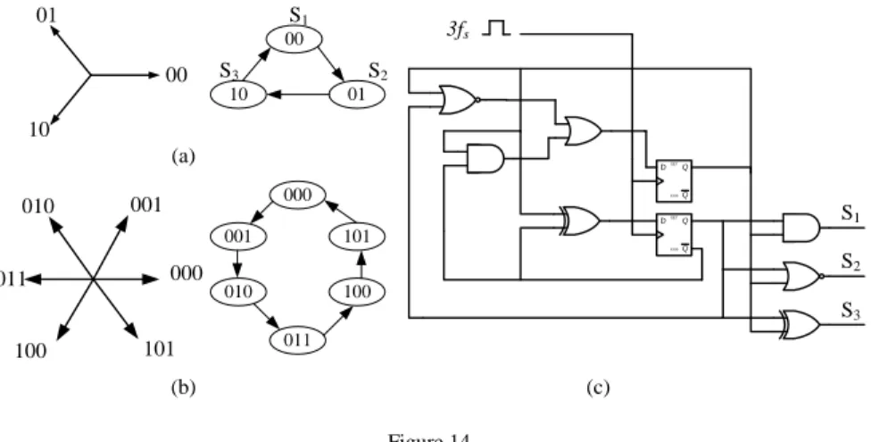
Due to three-pulse and six-pulse operation of the half-bridge and full-bridge inverters, the center frequency of the PLL must be close to three times and six times of the resonant frequency. Figure 14 shows the switching sequences for 1200 conduction mode for full-bridge and half-bridge topologies. Finally, the output of the VCO is connected to a sequential circuit to produce the proper switching sequences.
000 010
100
001
011
101 00 01
10
00
10 01
000
001 101
011
010 100
(a)
(b)
Q SETQ
CLR D
Q SETQ
CLR D
3fs
S1
S2
S3
(c) S1
S2
S3
Figure 14
(a) The three-step performance of sequential circuitfor half-bridge inverter; (b) six-step performance of sequential circuitfor full-bridge inverter; (c) the sequential circuit used for half-bridge inverter Figure 14(c) shows the proposed sequential circuit for the half-bridge topology.
To show the PLL dynamics, simulation results are carried out by PSIM simulator for the half-bridge topology. The parameters of the inverter and the PLL are listed in Table 1. Figure 15(a) shows the voltage of S1and the PLL dynamics at start-up.
Figure 15(b) shows output signal of the phase detector controller (or input signal of the VCO unit) at start-up. In these figures, the center frequency fc of the PLL is 65 kHz, which is approximately three times the resonant frequency. According to the resonant frequency, the final frequency of the VCO unit is close to 66 kHz.
In this simulation, the tolerances are less than 3% and the average value of the resonant frequencies is about 22 kHz. The parameters of the PI controller are set to achieve better dynamics. This simulation is done without power regulator.
However, by using a power regulator, the voltage stresses of the switches are significantly reduced at start-up,as in [24]. As seen from Figure 15, the output voltage of the controller has three steps for each switching period, which is three times faster thanconventional PD’s [21-25].
Table 1 Simulation parameters Resonant tank
parameters Inverter Parameters PLL specifications
Cr 330nF L1,2,3 600μH fc 65 kHz
Q ≈ 5 Vin 50V P
I KI= 5.5×10⁴, KP = 20
Lr 150μH - - τ 330μSec
fr ≈ 22 kHz - - K
V
1000 (Hz/Volt)
0 0.2 0.4 0.6 0.8 1.0 Time (ms)
0 0.5 1.0 0 50 100
(a)
(b)
Switch voltage (Volt)Controller output voltage (Volt)
Figure 15
(a) Voltage of S1 at start-up condition; (b) output signal of the PI controller at start-up condition
4 Experimental Results
A half-bridge inverterwas built and the performance of the inverter with the new PLL was investigated with operating frequency of 22 kHz. As mentioned, the structure of the PDis similar for the full-bridge and half-bridge inverters and the half-bridge topology is implementedfor simplicity. The parameters of the inverter and the PLL are listed in Table 2. In this prototype, the quality factor of the resonant tanks is investigated for 20 and 3. The quality factor of 20 is considered for the no-load condition. The center frequency of VCO is about 65 kHz for operating frequency of about 22 kHz.
Tolerance of theresonant inductor, Lr, is less than 1% and the resonant capacitors are metalized polypropylene film capacitor with maximum tolerance of 5%.
Therefore, according to (6), the maximum frequency deviationis less than 3% for each resonant tank. In this prototype, the equivalent load resistances are in series with resonant inductors for mentioned quality factors.
Figure 16(a) shows the performance of the new PLL at start-up condition. In this figure, the PLL’s center frequency is 65 kHz, which is approximately three times the average value of the resonant frequencies. The steady state switching frequency (or averaged value of three resonant frequencies) is about 22 kHz at quality factor of 20.
(a) (b)
(c) (d)
Figure 16
(a) Voltage of S1 at start-up condition by using the proposed tuning loop and input voltage of 20 V (10 volt/div); (b) gate to source voltage of the switches, (5 volt/div); (c) resonant tank current at quality factor of about 3, (500mA/div); (d) voltage of the switches at steady state condition and input voltage
of 20 V and quality factor of about 3, (20 volt/div) Table 2
Inverter and PLL parameters
Load parameters Inverter Parameters PLL specifications Cr ≈ 330 nF L1,2,3 600 μH fcenter ≈ 65 kHz Q ≈ 20 and 3 Series diodes BY399 PI KI ≈ 6×10⁴, KP ≈ 15 Lr ≈ 150 μH Switches IRFP540 τ 1000 μSec
fr ≈ 22 kHz Gate drivers ICL7667 KV 1000 (Hz/Volt) The PI controller of the PLL circuit is designed to achieve minimum phase error at steady state condition while the transient response is suitable. The optimum parameters of the PI controller are listed in Table 2. Figure 16(b) and (d) show the gating signals and the voltage of the switches at quality factor of about 3 with 3%
deviation. Figure 16(c) shows resonant tank current connected to S1 at the quality factor of 3 and output power of about 50 W. Figure 17 shows the laboratory prototype of the current source parallel resonant half-bridge inverterwith the resonant inductors and capacitors.
(a) (b) Figure 17
(a) The three resonant inductors and the resonant capacitor; (b) laboratory prototype of the current source parallel resonant half-bridge inverter
Conclusion
In this paper, a new PLL circuit is proposed for three-phase current source parallel resonant inverters. The new PLL tracks the average value of three resonant frequencies according to the new phase detector performance. This helps to achieve less voltage stresses on the switches and lower distortions in DC-link current. The PLL is investigated in multiplier phase and frequency mode to achieve fast dynamics at transients. The new tuning circuit uses only the voltage of the switches to detect the phase error and there is no feedback from the load currents. Therefore, the circuit is simple, more reliable and cost effective. The new PLL can be used for both full-bridge and half-bridge topologies while the sequential circuit difference must be taken in consideration.
References
[1] H. R. E. Larico and I. Barbi: Three-Phase Weinberg Isolated DC–DC Converter: Analysis, Design, and Experimentation, IEEE Transaction on Industrial Electronics, Vol. 59, No. 2, 2012, pp. 888-896
[2] G. A. Covic, J. T. Boys, M. L. G. Kissin and H. G. Lu: A Three-Phase Inductive Power Transfer System for Roadway-Powered Vehicles, IEEE Transaction on Industrial Electronics, Vol. 54, No. 6, 2007, pp. 3370-3378 [3] S. V. G. Oliveira and I. Barbi: A Three-Phase Step-Up DC–DC Converter
With a Three-Phase High-Frequency Transformer for DC Renewable Power Source Applications, IEEE Transaction on Industrial Electronics, Vol. 58, No. 8, 2011, pp. 3567-3580
[4] P. Alotto, A. Spagnolo and B. Paya: Particle Swarm Optimization of a Multi-Coil Transverse Flux Induction Heating System, IEEE Transaction on Magnetics, Vol. 47, No. 5, 2011
[5] J. Egalon, S. Caux, P. Maussion, M. Souley and O. Pateau: Multiphase System for Metal Disc Induction Heating: Modeling and RMS Current Control, IEEE Transaction on Industrial Application, Vol. 48, No. 5, pp.
1692-1699, 2012
[6] M. Daigavane, H. Suryawanshi and J. Khan: A Novel Three Phase Series- Parallel Resonant Converter Fed DC-Drive System, Journal of Power Electronics, Vol. 7, No. 3, 2007, pp. 22-232
[7] H. Matsumoto, Y. Neba, K. Ishizaka and R. Itoh: Model for a Three-Phase Contactless Power Transfer System, IEEE, Transaction on Power Electronics, Vol. 26, No. 9, 2011, pp. 2676-2687
[8] R. L. Andersen and I. Barbi: A Three-Phase Current-Fed Push–Pull DC–
DC Converter, Transaction on Power Electronics, Vol. 24, No. 2, 2011, pp.
358-368
[9] L. Pang, Y. Wang and T. Chen: New development of traveling wave induction heating, IEEE. Transaction on Applied Superconductivity, Vol.
20, No. 3, 2010, pp. 1013-1016
[10] Y. Hwang, B. Hwang, H. Lin and J. Chen: PLL-based Contactless Energy Transfer Analog FSK Demodulator using High Efficiency Rectifier, IEEE Transaction on Industrial Electronics, Vol. 60, No. 1, 2013, pp. 280-290 [11] R. L. Lin and C. H. Wen: Three-Phase Electronic Ballast with Current-
Equalization Function, Journal of Display Technology, Vol. 2, No. 4, pp.
378-385, 2006
[12] Z. Wang and H. Li: A Soft Switching Three-Phase Current-fed Bidirectional DC-DC Converter with High Efficiency over a Wide Input Voltage Range, IEEE Transaction on Power Electronics, Vol. 27, No. 2, 2012, pp. 669-684
[13] S. Lee, J. Park and S. Choi: A Three-Phase Current-Fed Push–Pull DC–DC Converter With Active Clamp for Fuel Cell Applications, IEEE Transaction on Power Electronics, Vol. 26, No. 8, 2011, pp. 2266-2277
[14] S. K. Changchien, T. J. Liang, J. F. Chen and L. S. Yang: Novel High Step- Up DC–DC Converter for Fuel Cell Energy Conversion System, IEEE Transaction on Industrial Electronics, Vol. 57, No. 6, 2010, pp. 2007-2017 [15] J. M. Kwon, E. H. Kim, B. H. Kwon and K. H. Nam: High-Efficiency Fuel
Cell Power Conditioning System With Input Current Ripple Reduction, IEEE Transaction on Industrial Electronics, Vol. 56, No. 3, 2009, pp. 826- 834
[16] B. Yuan, X. Yang, X. Zeng, J. Duan, J. Zhai and L. Donghao: Analysis and Design of a High Step-up Current-Fed Multiresonant DC–DC Converter With Low Circulating Energy and Zero-Current Switching for All Active Switches, IEEE Transaction on Industrial Electronics, Vol. 59, No. 2, 2012, pp. 964-978
[17] . Casanueva, C. ra as, . . Azcondo and . . D az: Teaching Resonant Converters: Properties and Applications for Variable Loads, IEEE Transaction on Industrial Electronics, Vol. 57, No. 10, 2010, pp. 3355-3363 [18] S. Jalbrzykowski and T. Citko: Current-Fed Resonant Full-Bridge Boost DC/AC/DC Converter, IEEE Transaction on Industrial Electronics, Vol. 55, No. 3, 2008, pp. 1198-1205
[19] A. L. Shenkman, B. Axelord and V. Chudnovsky: A New Simplified Model of the Dynamics of the Current-Fed Parallel Resonant Inverter, IEEE Transaction on Industrial Electronics, Vol. 47, No. 2, 2000, pp. 282-286 [20] M. K. Kazimierczuk, A. Abdulkarim: Current-Source Parallel-Resonant
DC/DC Converter, IEEE Transaction on Industrial Electronics, Vol. 42, No. 2, 1995, pp. 199-208
[21] N. Margaris and V. Petridis: Voltage Pump Phase-locked Loops, IEEE Transaction on Industrial Electronics, Vol. 32, No. 1, 1985, pp. 41-49 [22] A. Namadmalan and J. S. Moghani: Tunable Self-Oscillating Switching
Technique for Current Source Induction Heating Systems, IEEE, Transaction on Industrial Electronics, Vol. 61, No. 1, 2014, pp. 2556-2563 [23] H. Karaca and S. Kılınç: Nonlinear Modeling and Analysis of Resonant
Inverter Tuning Loops with Voltage-Pump Phase-Frequency Detector, IEEE, Transaction on Power Electronics, Vol. 20, No. 5, 2005, pp. 1100- 1108
[24] A. Namadmalan, J. S. Moghani and J. Milimonfared: A Current-fed Parallel Resonant Push-Pull Inverter with a New Cascaded Coil Flux Control for Induction Heating Applications, Journal of Power Electronics, Vol. 11, No. 5, 2011
[25] G. C. Hsieh and J. C. Hung: Phase-Locked Loop Techniques-A Survey, IEEE, Transaction on Industrial Electronics, Vol. 43, No. 6, 1996