Editors’ Suggestion
Coexistence of classical snake states and Aharonov-Bohm oscillations along graphene p-n junctions
Péter Makk,1,2,*Clevin Handschin,1Endre Tóvári,2Kenji Watanabe,3Takashi Taniguchi,3Klaus Richter,4 Ming-Hao Liu (),5and Christian Schönenberger1,†
1Department of Physics, University of Basel, Klingelbergstrasse 82, CH-4056 Basel, Switzerland
2Department of Physics, Budapest University of Technology and Economics and Nanoelectronics ‘Momentum’ Research Group of the Hungarian Academy of Sciences, Budafoki ut 8, 1111 Budapest, Hungary
3National Institute for Material Science, 1-1 Namiki, Tsukuba, 305-0044, Japan
4Institut für Theoretische Physik, Universität Regensburg, D-93040 Regensburg, Germany
5Department of Physics, National Cheng Kung University, Tainan 70101, Taiwan
(Received 30 March 2018; revised manuscript received 25 May 2018; published 9 July 2018) Here we present measurements on p-n junctions in encapsulated graphene revealing several sets of magnetoconductance oscillations originating from quasiclassical snake states and edge state Aharonov-Bohm interferences. Even though some of these oscillations have already been observed in suspended and encapsulated devices including different geometries, their identification remained challenging as they were observed in separate measurements, and only a limited amount of data was available. Moreover, these effects have similar experimental signatures, therefore for their proper assignment their simultaneous observation and their detailed characterization is needed. The investigation of the charge carrier density, magnetic field, temperature, and bias dependence of the oscillations enabled us to properly identify their origin. Surprisingly we have found that snake states and Aharonov-Bohm interferences can coexist within a limited parameter range. We explain this using a unified picture of magneto-oscillations and confirm our findings using tight binding simulations. Sincep-njunctions are the most important building blocks of graphene based electron-optical elements and edge state interferometers, our findings will be crucial for the design and understanding of future devices.
DOI:10.1103/PhysRevB.98.035413
I. INTRODUCTION
Magnetoconductance effects, the change of the conductance as a function of magnetic fieldB, are both of fundamental significance (e.g., Aharonov-Bohm effect, Shubnikov-de-Haas oscillations [1,2]) and important for applications (e.g., GMR [3,4], TMR [5], etc.). Such effects have been investigated to a great extent also in two-dimensional electron gases (2DEGs) realized in semiconductor heterostructures [1,2]. At low perpendicular magnetic fields electrons exhibit cyclotron motion that follows classical trajectories, allowing for the realization of electro-optical experiments such as transverse magnetic focusing [6,7]. At higher magnetic fields Landau levels are formed and electrons travel along edge channels [1,2]. Using electrostatic gating these channels can be guided within the sample, and using beam splitters based on quantum point contacts electronic Mach-Zehnder interferometers can be realized [8–10]. These interferometers enable the study of coherence effects of electronic states [11–13], noise in collision experiments [14,15], or probing the exotic nature of certain quantum Hall channels [16,17].
Graphene not only offers similarly high mobility as 2DEGs, but it also allows for the formation of gaplessp-ninterfaces not possible in conventional 2DEGs. Graphenep-njunctions host quasiclassical snake trajectories at low field [18–23], where
*Peter.makk@unibas.ch
†Christian.Schoenenberger@unibas.ch
electrons curve back and forth along the opposite side of the p-njunction. At high field edge channels propagate along the junction and coupling between these channels result in a Mach- Zehnder interferometer displaying the Aharonov-Bohm effect [24,25]. Both effects result in magnetoconductance oscillations as a function of magnetic field and gate voltage. However, their similar signatures make it difficult to distinguish the two from each other. Moreover, experiments are performed within the transition between the classical and the quantum regime.
Finally, Coulomb interaction of charge carriers localized in conducting islands coupled to edge channels can also lead to magnetoconductance oscillations [26–29].
Here we present measurements on high-mobility encapsu- lated graphenep-njunctions, where several sets of magneto- conductance oscillations are observed simultaneously. A part of these oscillations has been observed [21,22,24,25], but there is still an ongoing discussion on their origin. Usually only a limited amount of measurement data is available which makes their analysis challenging and can lead to misinterpretation of their origin. Their simultaneous observation, which we report here, as well as their detailed characterization as a function of gate, magnetic field, temperature, and bias voltage, allows for their direct comparison, resulting in a unified picture and a consistent assignment of the different oscillations. Whereas previously it was believed that snake states and Aharonov- Bohm oscillations appear in quite a different parameter regime, here we show that they can coexist for certain parameters.
We describe our findings taking into account the role of local electric fields at thep-njunction and discuss a quantum model
of snake states based on quantum Hall channels. Our findings are confirmed by tight binding simulations.
The paper is organized as follows: First we introduce the most relevant concepts of snake states and Aharonov-Bohm oscillations along graphene p-n junctions. Then we present measurements of several sets of oscillations within the bipolar regime. These magnetoconductance oscillations are carefully analyzed with respect to their gate, magnetic field, temperature, and bias dependence. We show that these oscillations can be attributed to either snake states or Aharonov-Bohm oscillations as introduced previously. We furthermore support our findings with theoretical models and quantum transport simulations.
Finally, we briefly discuss an additional type of magnetocon- ductance oscillation that has not been reported before.
A. Snake states
In small magnetic fields electrons follow skipping trajecto- ries which turn to snake states along thep-njunction [19–22].
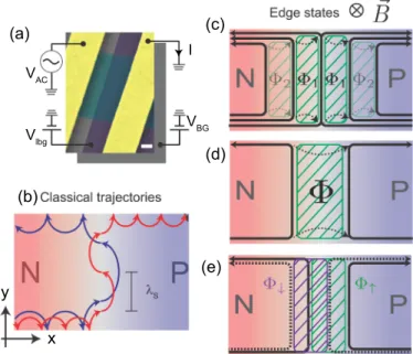
These trajectories bend in the opposite direction on the two sides of thep-njunction due to an opposite Lorentz force, as sketched in Fig.1(b). Charge carriers with trajectories having a small incident angle with respect to thep-njunction normal are transmitted very effectively from then- top-doped region of the graphene device (and vice versa) due to Klein tunneling [30–32]. In the simplest case thep-njunction is steplike and symmetric, and the cyclotron radius,RC=λS/2=hk¯ F/(eB), is the same constant value on both sides. Here kF is the momentum of the electrons,B the magnetic field, andλSis the size of the snake period or “skipping length.” By changing Bor the electron densityn, and thus the cyclotron radius, the charge carriers end up either on the left or right side of thep-n junction, similar to what is shown in Fig.1(b). This results in a conductance oscillation, where the conductance is determined by how the cyclotron radius compares to the length of thep-n junction.
A more realistic model includes a gradual change of the charge carrier density across the p-n junction, which is illustrated in Fig. 1(b). For ap-n junction parallel to they direction this gives rise to a position-dependent electric field Ex (which in the case of constantEfield would lead to the well knownE× Bdrift velocity). By solving the semiclassical equations of motion for an idealized graphenep-njunction where the charge carrier density changes linearly fromnL to nR over a distance of dn, the skipping lengthλS is given by (see Supplemental Material (SM) [33]):
λS= πh¯
eB 2
|nL−nR|
dn . (1)
Note thatS= |nL−nR|/dn corresponds to the slope of the charge carrier density profile. The conductance oscillations which can be measured across thep-njunction of widthWat a given Fermi energyEcan be described by a phenomenological model according to:
G(E)∼cos
πW λS
, (2)
which describes the commensurability betweenλSandW. The cosine itself accounts for a smooth conductance oscillation.
Details of this model will be discussed later. We emphasize
FIG. 1. Concept of snake states and Aharonov-Bohm interference along a graphene p-njunction. (a) False-color SEM image of the device where the leads are colored yellow, the graphene encapsulated in hBN is colored cyan, and the local bottom gate (a structured few- layer graphite electrode underneath the hBN-graphene-hBN stack) is colored purple. Scale bar equals 200 nm.VBGdenotes the voltage applied to the global back gate andVlbgis applied to a graphite bottom gate. (b) Snake states seen in the framework of classical skipping orbits for two different magnetic field values (blue and red trajectories, Bred> Bblue). (c) Principle of Aharonov-Bohm interference between quantum Hall edge states propagating along thep-n interface. At high bulk filling factors (νL/R) several different areas are enclosed due to interchannel scattering at the flake edges (green shaded area and dashed arrows). Of these, the one that involves the least number of scattering events is expected to dominate (1). (d) At high magnetic fields Aharonov-Bohm interference can occur between the spatially separated edge states of the degeneracy-lifted lowest Landau level.
The green area corresponds to the insulating region with localν of 0. (e) At even larger magnetic fields full degeneracy lifting occurs, and two spin-polarized interferometers are formed: purple area for spin-down (dashed) channels, green for spin-up (solid) channels. The interferometers are independent, as scattering between them is not allowed, since the spin is conserved along the edges.
again that phase coherence is not required for this effect to appear.
B. Aharonov-Bohm oscillations
While at low magnetic fields the motion of the charge carriers is well described using the picture of skipping and snake trajectories along edges andp-njunctions, upon increas- ing the magnetic field one enters the quantum regime where transport is commonly described by edge states. The concept of interference formed by spatially separated edge states has already extensively been studied in 2DEGs, including the realization of Fabry-Pérot [49] and Mach-Zehnder [8]
interferometers, while in graphenep-njunctions it was first introduced by Morikawaet al.[24]. Here, edge states propagate on either side of the p-n junction, and coupling between them is enabled at the junction’s ends due to scattering on
disordered graphene edges as illustrated in Figs.1(c)and1(d).
Coupling between the edge states across the p-n junction, illustrated in Fig.1(c)by the black, dashed arrows, is restricted to the disordered graphene edges [24,25]. As the edge states encircle an enclosed areaAat finite perpendicular magnetic fieldB, the acquired Aharonov-Bohm phase is the magnetic flux,=AB. The conductance oscillations can be described phenomenologically:
G(E)∼cos
2π
0
, (3)
where0=h/e is the magnetic flux quantum [50]. In contrast to snake states, this is a phase coherent effect.
If multiple Landau levels are populated, several different interferometer loops, enclosing different areas, can contribute.
However, for the measured conductance across thep-njunc- tion only paths that connect thento thepside are relevant. Of these, the ones with the least number of scattering events are expected to dominate the oscillation. These are the two inner ones denoted with1 in Fig. 1(c). The interference signal involves only one scattering event along each path, while for loops of type2 at least two scattering events are necessary per path.
At high magnetic fields the Landau levels, which have valley and spin degeneracy at low field, can be partially (or fully) split [51,52]. This leads to a spatial separation of the edge states associated with the lowest Landau level by an insulating region (ν=0), as shown in Fig.1(d). Here, the valley degeneracy is lifted so that the edge state is still spin degenerate.
The idea of an Aharonov-Bohm interference, put forward in Ref. [24], was generalized by Weiet al.[25] by considering full degeneracy lifting of the Landau levels, both in spin and valley. It was shown that the edges can mix the valleys, but not the spins, as sketched in Fig.1(e). Therefore scattering between edge states is only possible if they are of identical spin orientation. This gives rise to two sets of magnetoconductance oscillations—one for each spin channel for bulk filling factors
|νL/R|>2 as described in Ref. [25]. An increase of the spacing between neighboring edge states is expected to decrease the scattering rate at the flake edge between edge states, giving rise to a reduced oscillation amplitude. At the same time the magnetic field needed to change the flux by a flux quantum is reduced, which will lead to changing magnetic field spacing.
Details of the magnetic field spacing and the temperature dependence of the Aharonov Bohm will be discussed later.
II. MEASUREMENTS
The hBN/graphene/hBN heterostructures were assembled following the dry pickup technique described in Ref. [53]. The full heterostructure was transferred onto a prepatterned piece of few-layer graphene used as a local bottom gate. Standard e-beam lithography was used to define the Cr/Au side contacts, with the bottom hBN layer (70 nm in thickness) not fully etched through in order to avoid shorting the leads to the bottom gates. The graphene samples were shaped into 1.5μm wide channels using a CHF3/O2plasma. A false-color SEM image of the final device is shown in Fig.1(a)(for more details see SM [33]). The charge carrier mobilityμwas extracted from field effect measurements yieldingμ∼80 000 cm2V−1s−1.
Thep-njunction is formed by a global back gate and a local bottom gate which allows for independent tuning of the doping on each side of thep-njunction. The presence of Fabry-Pérot oscillations (see SM [33]) also attests to the high quality of our device. We have observed the magnetoconductance oscillations on ∼10 p-n junctions in two separate stacks.
Measurements were performed in a variable temperature insert with a base temperature of T =1.5 K and a He-3 cryostat with a base temperature ofT =260 mK, using standard low- frequency lock-in techniques.
A. Gate-gate dependence
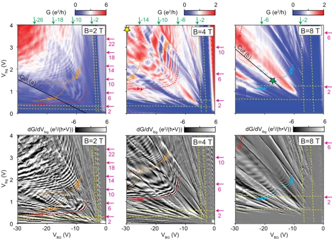
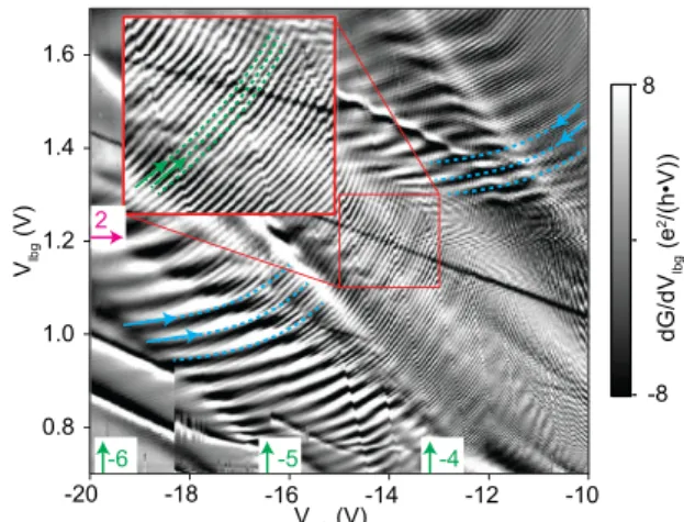
In Fig.2the two-terminal conductance (top panels) and its numerical derivative (bottom panels) are shown as a function of the global back gate (VBG) and the local bottom gate (Vlbg) within the bipolar regime at selected magnetic fields. Zero voltage of the global back gate or local bottom gate corresponds roughly to zero doping in the left or right side of the sample.
In the gate-gate map, fine curved lines are visible along which the conductance is approximately constant, and perpendicular to these lines the conductance oscillates. Within the measured gate and field range we identify three different types of magne- toconductance oscillations which are labeled with red, orange, and cyan arrows/dashed lines. All of them have a roughly hyperbolic line shape being asymptotic with the zero-density lines related to either of the two sides of the samples. However, they are observed within different parameter ranges. The filling factorsν=nh/(eB), corresponding to the bulk values of the two sides tuned by the global back gate and local bottom gate, are indicated with the green and purple arrows in Fig.2. The yellow dashed lines correspond to |ν| =1 and |ν| =2, for either side.
Upon comparing the different magnetoconductance os- cillations it can be seen that the cyan ones exist at very low filling factors (starting at |ν|>1), the red ones exist at intermediate filling factors (νBG,νlbg)∼(−4,4), and the orange ones appear at the highest filling factors. For one orange set, the filling factor values where the oscillations start to appear are around (νBG,νlbg)∼(−4,8), for the other orange set around (νBG,νlbg)∼(−8,4). Furthermore, the spacing of neighboring conductance oscillations as a function of charge carrier doping differs significantly for the cyan, red, and orange oscillations. An additional conductance modulation is also present where high and low conductance values follow lines that fan out linearly from the common charge neutrality point.
The effect is more pronounced at higher magnetic fields and was attributed to valley-isospin oscillations [54–56] which are discussed in detail in Ref. [57].
Whereas for the red magnetoconductance oscillations only one set is observed, two sets are observed for the orange and cyan ones. The latter ones are furthermore shifted in doping with respect to each other. Using a device with a geometry enabling gate definedp-n-porn-p-njunctions (see SM [33]) we have excluded the possibility that the two orange sets of magnetoconductance oscillations originate from an additional p-n junction formed between n-doped graphene near the Cr/Au contacts and ap-doped bulk. This is in agreement with quantum transport simulations (discussed later in this paper), which reproduce a double set of oscillations, in the same
FIG. 2. Conductance (top panels) and its numerical derivative (bottom panels) of ap-njunction in the bipolar regime for different magnetic fields. The filling factors, obtained from a parallel-plate capacitor model, are given in green for the cavity tuned by the global back gate (νBG) and in purple for the cavity tuned by the local bottom gate (νlbg). The yellow, dashed lines indicate filling factors 1 and 2. The different types of magnetoconductance oscillations are indicated with the red, orange, and cyan arrows/dashed curves. The lines indicate where the magnetic field dependencies of Fig.3were taken, whereas the stars indicate the position of the bias dependent measurements of Fig.5.
range where the orange ones are observed, without introducing contact doping. Therefore, a double set of oscillations must be the sign of two different interferometer loops working simultaneously near thep-njunction in the bulk [see Fig.1(b)].
B. Magnetic field dependence
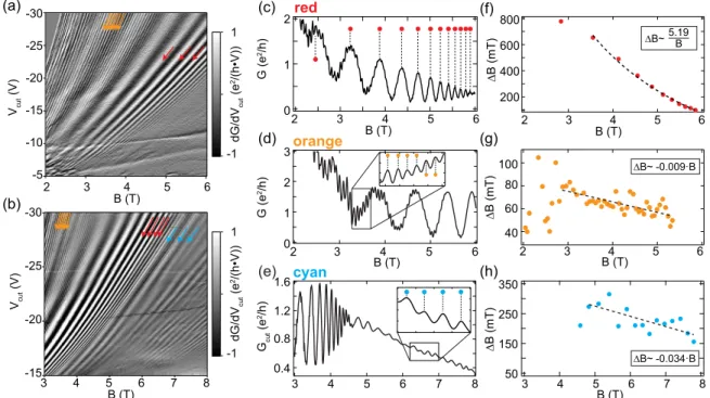
Next we measured selected line cuts as indicated in Fig.2 with “Cut (a)” and “Cut (b)” as a function of magnetic field.
The differential conductances as a function of magnetic field and gate voltage are shown in Figs.3(a)and3(b). The three magnetoconductance oscillations, which are labeled with the red, orange, and cyan arrows, follow a roughly (but not exactly) parabolic magnetic field dependence where the oscillations shift to higher absolute gate voltages with increasing magnetic field. Furthermore, we observe a coexistence of multiple oscillations within a limited parameter range. The coexistence of the red and orange oscillations is seen in both Fig.3(a) and Fig.3(b). The conductance as a function of the magnetic field, while keeping the charge carrier densities on both sides of thep-njunction fixed, is plotted in Figs.3(c)–3(e)for three selected configurations. In Figs.3(c)and3(d)large oscillations (red in the previous graphs) with peak-to-peak amplitudes reaching nearly 2 e2/h can be seen. Within a limited parameter range there are smaller oscillations (orange in the previous graphs) superimposed on top of the red oscillations, having
amplitudes reaching up to ∼0.6 e2/h. The cyan oscillations show amplitudes in the range∼0.05–0.1 e2/ h. The magnetic field spacing (B) between neighboring peaks is given in Figs. 3(f)–3(h) for the corresponding oscillations shown in Figs. 3(c)–3(e). Even though all three types of magnetocon- ductance oscillations reveal a different spacing ofB, they share a common trend, namely the decrease of B with increasing B. Nevertheless, the rate of B as a function of B is quite different for the red compared to the orange and blue magnetoconductance oscillations, which is an indication that different physical mechanisms are involved.
C. Temperature dependence
In Fig.4the temperature dependence of the red, orange, and cyan magnetoconductance oscillations is given. Figure 4(a) shows the red oscillations as a function of gate voltage and temperature (|nBG| ∼ |nlbg|andB=3.5 T). We characterize the temperature dependence of each oscillation by calculating the area A under the oscillation with respect to the high-T smooth background. From this the normalized area, which is defined asAnorm.=A(T)/A(T =1.6K), can be extracted at different densities, and is plotted as a function of temperature in Fig.4(b). A characteristic temperature for the disappearance of the oscillations,Tc, is then defined according toAnorm(Tc)= 0.1. In Fig.4(c),TCis plotted as a function of the density for all
FIG. 3. Magnetic field dependence. (a) Numerical derivative of the conductance as a function of magnetic field and gate voltage as labeled in Fig.2with “Cut (a).” Within a limited parameter range the magnetoconductance oscillations indicated with the red and orange arrows coexist. The latter can be better seen in (b), along the line cut labeled in Fig.2with “Cut (b).” (c)–(e) Conductance as a function of magnetic field for representative gate-gate configurations of the red (VBG= −20 V,Vlbg=1.8 V), orange (VBG= −27.5 V,Vlbg=4 V), and cyan (VBG= −18.5 V,Vlbg=1.27 V) magnetoconductance oscillations. The peak positions are indicated with the red, orange, and cyan dots.
(f)–(h) Magnetic field spacing between successive peaks (B) extracted from (c)–(e). A 1/Band linear dependence ofBas a function ofB is indicated with the black dashed curve/lines for the snake states and Aharonov-Bohm interferences, respectively.
FIG. 4. Temperature dependence. (a) Red magnetoconductance oscillations as a function of the global back gate (Vlbgis chosen such that|nBG| ∼ |nlbg|) and temperature atB=3.5 T. (b)Anormof the red oscillations [the dominant ones in (a)] is plotted here as a function of temperature at various densities. The color coding corresponds to thexaxis of panel (a). (c) The solid lines/dots show the experimental values ofTC, defined as the temperature for which the oscillation amplitude is reduced to 10% of its low temperature value of the red, orange, and cyan magnetoconductance oscillations (extracted atB= 3.5 T,B=3 T, andB=8 T, respectively) as a function of charge carrier doping. The red, dashed line corresponds to the vanishing of snake states according to equation (6) using dn=50 nm and W=1500 nm.
three types of magnetoconductance oscillations. While the red magnetoconductance oscillation reveals a significant temper- ature dependence as a function of the charge carrier density, surviving up to T ∼100 K at high doping, the orange and cyan magnetoconductance oscillations vanish at temperatures around T ∼10 K irrespective of the charge carrier density.
This suggests again that different mechanisms are responsible for the red magnetoconductance oscillations compared to the orange and cyan magnetoconductance oscillations. Ballistic effects, such as snake states and transverse magnetic focusing, are known to survive to temperatures up to T ∼100 K to 150 K [7,22,58]. On the other hand, phase coherent transport in similar devices vanishes at temperatures around∼10 K (see Ref. [59]).
D. Bias dependence
We have also investigated the bias dependence of the differ- ent oscillations as a function of magnetic field while keeping the charge carrier densities fixed. The bias was applied asym- metrically at the source, while the drain remained grounded.
The red magnetoconductance oscillations evolve from a tilted line pattern at smaller magnetic fields into a checkerboard pattern at high magnetic field as shown in Fig.5(a)(a smooth background is subtracted). At high magnetic field the visibility of the checkerboard pattern decreases with increasing VSD while a similar behavior is absent (within the applied bias range of±10 mV) for the tilted pattern. The bias dependence of the orange and cyan magnetoconductance oscillations is
FIG. 5. Bias spectroscopy. (a)–(c) Measurement of the red, orange, and cyan magnetoconductance oscillations as a function of bias and magnetic field where a smooth background was subtracted. Gate voltages remain fixed and are indicated in Fig.2with the yellow (red and orange oscillations) and green (cyan oscillation) stars. (d)–(f), Phenomenological simulations of the bias dependence of snake state and interference-induced oscillations (a)–(c). Parameters used:W=1.5μm,dn=100 nm (red oscillations),kFcorresponding ton∼1.7× 1012cm−2(red, orange) orn∼0.8×1012cm−2(cyan). For the Aharonov-Bohm oscillations we considered a bias dependent gating effect with α=0.32 nm/mVSDandd=40 nm (orange oscillation) orα=0.25 nm/mVSDandd=20 nm (cyan oscillations), while a renormalization of the edge state velocity is neglected (β=1).
shown in Figs. 5(b) and 5(c), both revealing a tilted line pattern within the measured magnetic field range, as shown by the dashed lines and arrows. The bias dependence of the orange oscillations persists to ±10 mV, whereas that of the cyan oscillations vanishes around roughly±2 mV. In Fig.5(c) additional magnetoconductance oscillations with a narrow spacing of roughly B ∼4 mT to 6 mT can be observed, indicated by green arrows and green dashed lines. These oscillations will be briefly discussed at the end of the paper.
III. DISCUSSION
We have observed different magnetoconductance oscilla- tions, marked with red, orange, and blue. All of the oscillations have roughly hyperbolic line shapes in the gate-gate map, but the magnetic field spacing, the temperature dependence, and the fact that there is only a single set of red oscillations suggest that they are governed by different physical mechanisms.
Based on the experimental evidence presented until now, it is suggestive to assign the red oscillations to snake states and the others to the Aharonov-Bohm effect. This will be substantiated further on below.
A. Magnetoconductance oscillations marked in red The red magnetoconductance oscillations start to appear in the range|ν| ∼3–6 as can be seen in Fig.2. This corresponds to an occupation of roughly two edge states (ν= ±4, Landau levels 0 and±1) without taking degeneracy lifting into account.
The shape of the red magnetoconductance oscillations fits very well to what is expected for snake states following equation (1) and equation (2), as we will show below.
As discussed in the introduction, the oscillation results from a commensurability relation of the p-n junction length and
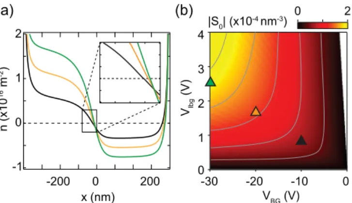
the skipping length, where the conductance is high or low depending on whether the snaking trajectories end up on the source or the drain side. If the magnetic field is fixed, the skipping length λS is directly proportional to the slope of the p-n junction according to equation (1). In Fig. 6(a) the calculated charge carrier density profile atB=0 T is shown for three exemplary gate-gate configurations (details of the electrostatic simulations are given in the SM [33]). It is clear thatS0characterizes well the density profile in the vicinity of thep-njunction.S0as a function of gate voltages is plotted in Fig.6(b): Here curves of constantS0, and therefore of constant λS(ifBremains fixed), follow a roughly hyperbolic line shape in agreement with the shape of the red magnetoconductance
FIG. 6. Charge carrier density profile in the bipolar regime and extracted slope. (a) Representative charge carrier density profiles calculated from electrostatics at positions as indicated in (b) with the triangles. Atn=0 the slope is nearly linear (inset). (b) Slope|S0| extracted atn=0 as a function of the gates. Gray curves represent constant values of|S0|, and consequently ofλS, as well [equation (1)].
oscillations (Fig.2). Although the orange and cyan oscillations also seem to follow hyperbolic shapes on gate-gate maps, the red ones only have a single set as expected of snake states.
Next we analyze the magnetic field dependence and spacing expected of snake state induced oscillations. Based on S0 [Fig.6(b)] one can calculate the conductance contribution as a function of an arbitrary line cut and magnetic field (not shown here), leading to a roughly parabolic magnetoconductance oscillation which strongly resembles the measurements shown in Figs.3(a)and3(b).
By using the model with a constant density gradient the magnetic field spacing as a function of magnetic field is given approximately by (see SM [33]):
B∼2π2h¯2n e2W dn
1
B, (4)
where a symmetric p-n junction with n≡ |nL| = |nR| was assumed. The magnetic field spacing in the experiment is very well described by the 1/B dependence. By fitting the magnetic field spacing of the snake state model as described in equation (4) to the measurements shown in Fig. 3(f) we extracted a slope ofS=1.82×10⁻³nm−3which is roughly one order of magnitude larger than what was calculated in Fig.6(b) (S0 ∼1.2×10⁻⁴nm−3). One explanation for the discrepancy is that strictly speakingS0is only valid atB =0 T.
However, at finite magnetic field the charge carrier density has to be calculated self-consistently leading to areas with a constant charge carrier density (compressible region) and areas where the charge carrier density changes rapidly (S > S0, incompressible regions) [60]. Also, the model supposes that the trajectories stay within the area with a constant density slope (see SM [33]), which might be not valid at low fields due to the increased cyclotron radius and skipping length.
The decrease of the oscillation amplitude with increasing magnetic field [Fig.3(c)] is compatible with the picture of classical snake trajectories, where the conductance oscillation results from the sum over all trajectories which form caustics along thep-njunction [61,62]. Upon increasing the magnetic field the charge carriers have to pass thep-njunction more often (decreasing λS). This leads to a reduced oscillation amplitude [23] because only trajectories with an incident angle being perpendicular to thep-n junction (θ =0) have a transmission probability oft =1, while for all remaining trajectoriest <1 is valid [31,32,63].
Our most compelling argument for identifying the red oscillations with snake states comes from the comparison of the measured temperature dependence with that calculated by the following simple model. At finite temperaturesT the Fermi surface is broadened byE∼kBT (where kB is the Boltzmann constant), thus leading to a spread of the Fermi wave vector according tokF∼kBT /( ¯hvF). The oscillations are expected to vanish if the smearing of trajectories becomes comparable to half a period:
2(λS,max−λS,min)·N∼ λS, (5) where λS,max, λS,min, and λS correspond to the maximal, minimal, and average skipping length, respectively, andN to the number of skipping periods. This leads to a characteristic
temperature
Tc≈ 2vFh¯3 W dnkBe2B2
√n3π5, (6)
where the oscillations vanish. Here kB is the Boltzmann constant. Details of the calculation can be found in the SM [33].
The vanishing of the red magnetoconductance oscillations with increasing charge carrier doping, which is plotted in Fig.4(c) (red, dashed line), is in good agreement with what is expected for snake states according to Eq. (6), unlike the other type of oscillations.
Finally, we analyze the bias dependence of snake states.
Details of the model can be found in the SM [33]. The bias dependence is calculated by taking into account the energy dependence of the snake period through its momentum dependence. In the case of a fully asymmetric bias the model reproduces the tilted pattern which is shown in Fig.5(d)at low magnetic field. On the other hand, for the case of completely symmetric bias, the same model leads to the checkerboard pattern which is shown in Fig. 5(d) at high magnetic field.
The checkerboard pattern is in agreement with previous studies [24,25], where a similar behavior was observed. The oscillation period decreases with increasing magnetic field in the simu- lation [Fig. 5(d)] comparable to the experiment [Fig. 5(a)].
In order to reproduce the transition from tilted (asymmetric biasing) to checkerboard pattern (symmetric biasing) we varied the bias asymmetry going from low to high magnetic field. We speculate that it might be related to the capacitances in the system [64], but the precise reason remains unknown so far.
We discuss this in more detail in the SM [33].
B. Magnetoconductance oscillations marked in orange From all the observed magnetoconductance oscillations the orange ones occur at the highest filling factors starting at roughly|ν| ∼6 and persisting up to|ν| =20 or even higher, as shown in Fig.2. This corresponds to an occupation of at least two edge states (|ν| =0 and|ν| =4) without taking a possible degeneracy lifting into account. Snake states can be excluded here, as the double set of oscillations indicates two simultaneous effects, with their origin displaced in real space with respect to thep-njunction. Therefore, we attribute these oscillations to Aharonov-Bohm oscillations between quantum Hall edge states propagating in parallel with each other and the p-njunction. Their temperature,B-field and bias dependence also support this idea. Below we discuss expectations and compare them with our experimental observations.
In an Aharonov-Bohm interferometer, the magnetic field spacingBbetween neighboring conductance peaks is given by:
B= h e
1
A. (7)
Here 0=h/e is the magnetic flux quantum and A is the enclosed area given by the product of the width of the flakeW and the distance of the edge statesd.
This suggests a constantBfor a fixed spacingd. However, in the experiments B is not exactly constant because the real-space positions of the edge states, which defineA, vary as a function of magnetic field and the p-n junction’s density
profile [24]. By considering a linear charge carrier density profile B decreases linearly with increasing B. This is in agreement with what was measured in Figs. 3(g)and 3(h), indicated with the black dashed line, therefore suggesting an Aharonov-Bohm type of interference. Even though multiple areas might be enclosed between the various edge states, only one Aharonov-Bohm loop will dominate as explained previ- ously and sketched in Fig.1(b). The magnetic field spacing of the orange magnetoconductance oscillations [Fig.3(g)] was converted into a distance ranging from d∼30 nm at B ∼ 2 T to d ∼55 nm atB ∼5.5 T. The decreasing oscillation amplitude (Gosc) with increasing magnetic field [Fig.3(d)]
directly indicates the vanishing coupling between edge states as they move further apart from each other at higher magnetic fields.
We have used the zero-field electrostatic density profile shown in Fig. 6(a) to identify the spacing d between two edge states for any set of (VBG,Vlbg) within the gate-gate map.
The magnetoconductance oscillation can then be calculated according to equation (3), leading to a roughly hyperbolic shape as a function of the two gates at fixed magnetic field (see the Supplemental Material). The two sets of the orange oscillations can be reproduced with a double Aharonov-Bohm interferometer as sketched in Fig.1(b), where the conductance oscillations arising from the interferometer on the left (e.g., quantum Hall channel withν=0 andν= ±4) and right (e.g., ν=0 andν= ∓4) side are added up incoherently. The two sets of orange magnetoconductance oscillations are slightly shifted in doping with respect to each other because each of the two gates tunes one side of thep-njunction more effectively.
Furthermore, measuring a line cut as a function of magnetic field reveals a roughly parabolic trend (see SM [33]). These findings are in good agreement with the measurements which are shown in Fig.2and Figs.3(a)and3(b), respectively.
In interference experiments which depend on phase co- herent transport, a vanishing of the oscillation pattern with temperature can have different origins such as loss of phase coherence due to enhanced inelastic scattering events. As soon asl< L, wherelis the phase coherence length andLis the total path length, the interference pattern is almost completely lost. As mentioned before, the phase coherence length is below 1–2μm in similar devices at temperatures around∼10 K (see Ref. [59]). However, the interference can as well be lost at finite temperatures even ifl > Lif the two interfering paths have different lengths (L=0), again due to the smearing of the Fermi wave vector. In this case, the interference pattern is expected to vanish at temperatures around
T = hvF
kBL. (8)
Since for the Aharonov-Bohm interference along a graphenep-njunctionLis ideally zero [see Figs.1(b)and 1(c)] or very small, this effect is negligible. Consequently, the loss of the interference signal with increasing temperature depends on the decrease ofl, which depends only weakly on the charge carrier doping [59], in agreement with Fig.4(c).
Finally, we calculate the bias dependence of Aharonov- Bohm oscillations. The details of the model are discussed in the SM [33]. The bias dependence is introduced via the momentum
difference which leads to:
G(V)∼cos
2πW ·(d+αV)·B
0 +kL
. (9) Hereαis a phenomenological parameter in order to account for a bias dependent gating effect [11]. For simplicity the edge state spacingd is modified proportional to the applied bias. The factor kL in Eq. (9) accounts for a possible path difference between the edge states, wherek is replaced by k=kF+eV /( ¯hvFβ). The parameter β (0β 1) was introduced to account for the renormalized edge state velocity compared to the Fermi velocity [65].
We have found that the second term alone (kLatα=0) cannot lead to substantial bias dependence if the parameters are chosen realistically (L∼20 nm andβ =1). To account for the tilt of the measurement a considerable renormalization of the edge state velocity is needed leading to an unphysically large reduction ofvF by a factor of one hundred. Therefore most of the tilt must come from nonzeroαand the bias induced gating effect.
The applied bias voltage shifts the electrochemical potential on one side (or both sides) and therefore leads to a change of the density profile. The changing density profile results in shifting of the edge states, and in order to keep the flux through the inter- ferometer fixed, the magnetic field has to be changed. Assum- ing that the applied bias affects the edge state spacing according tod=α·VSD, thenαcan be extracted from the bias spacing in Fig.5(b). This leads to values ofα∼ 0.32 nm/mVSD. The resulting bias dependence is plotted in Fig. 5(e). Based on a simple model, it is possible to numerically estimate the value of alpha, to compare with the observation. We keep the width dnof thep-njunction constant and take the bias voltage into account directly changing the left and right band offset and thus nL/R. From this simple model we obtain values in the order of α∼0.39 nm/mVSDto 0.48 nm/mVSDfor the orange magne- toconductance oscillations, which agrees fairly well with the experimental observations. Details are given in the SM [33].
C. Magnetoconductance oscillations marked in cyan The cyan magnetoconductance oscillations were observed at the lowest filling factors as low as|ν| ∼2 or even less, above B ∼4 T as shown in Fig.2. We attribute these oscillations to Aharonov-Bohm oscillations formed by edge channels of the fully degeneracy lifted lowest Landau level, as shown in Fig.1(e). Since full degeneracy lifting of the lowest Landau level (valley and spin) is observed forB >5 T (see SM [33]), the edge states are spin and valley polarized. While the spin degree of freedom is conserved along the edges of graphene and along thep-njunction [25], the valley degree of freedom is only conserved along the p-n junction. Mixing between the edge states of the lowest Landau levels having equal spin is consequently prohibited along the p-n junction, but possible at the graphene edges. Comparable to the orange mag- netoconductance oscillations, the magnetic field spacing of the cyan oscillations decreases monotonically, corresponding to an edge state spacing of d ∼9 nm at B=4.5 T and to d ∼15 nm atB=8 T. The oscillation amplitude of the cyan magnetoconductance oscillation shown in Fig.3(c)was rather constant with magnetic field including some irregularities.
We note that the cyan magnetoconductance oscillations are predominantly visible at a charge carrier doping of|nBG| ∼
|nlbg|(Fig.2) for reasons which are unknown yet. Similar to the orange magnetoconductance oscillations, the temperature dependence of the cyan ones depends only slightly on the charge carrier density and is most likely related to the loss of phase coherence.
Finally, the bias dependence is modelled similarly to the orange oscillation. The measurements can be well reproduced by usingα∼0.25 nm/mVSDto account for the bias dependent gating effect as demonstrated in Fig.5(f), which shows good agreement with our measurements [panel (c)]. Our simple estimate using the model detailed in the SM [33] gives values in the order ofα∼0.16 nm/mVSDto 0.25 nm/mVSDfor the cyan magnetoconductance oscillations, again agreeing fairly well with the experimental findings.
IV. QUANTUM TRANSPORT SIMULATIONS To complement our measurements, we additionally per- formed quantum transport calculations based on so-called scaled graphene [66] using the realistic device geometry.
These calculations were able to reproduce the red and orange magnetoconductance oscillations. In the calculations electron- electron interactions are not taken into account. In Fig.7(a) the conductance is shown as a function of the local bottom gate and the global back gate atB=3 T within the bipolar regime. Comparable to the measurements presented in Fig.2, two sets of magnetoconductance oscillations can be seen which are shifted in doping, which we identify with the orange ones. A few ridges also appear which we assign to the red oscillations.
In Fig.7(b)the evolution of the red and orange oscillations are shown as a function of gate and magnetic field. The calculations show that the orange magnetoconductance oscillations seen in the experiments can be reproduced without the splitting of
FIG. 7. Quantum transport calculations for a graphenep-njunc- tion in magnetic field. (a) Transmission function (T) of charge carriers through thep-njunction with the same gate geometry as measured one, as a function of a local bottom gate and a global back gate.
Red and orange magnetoconductance oscillations are indicated with the dashed curves/arrows. Filling factors of the global back gate and the local bottom gate are indicated with the green/purple arrows.
Low doping values (shaded in gray) were omitted to reduce the computational load. (b) Line cut as indicated in (a) with the black line as a function of magnetic field.
FIG. 8. Additional magnetoconductance oscillations at high mag- netic field. Numerical derivative of the conductance as a function of the global back and local bottom gates at B=8 T where two additional sets of fine oscillations can be observed (indicated with the green, dashed line), superimposed on each set of cyan oscillations.
Left and right side filling factors are indicated by green and purple arrows, respectively.
the lowest Landau level in contradiction with the claims of Ref. [25]. In that work all oscillations were linked to the split lowest Landau levels, however our analysis shows that only the blue oscillations, appearing at the lowest filling factors, can be attributed to degeneracy lifted Landau levels.
V. ADDITIONAL MAGNETOCONDUCTANCE OSCILLATIONS AT HIGH MAGNETIC FIELD Two additional sets of magnetoconductance oscillations that have been observed already in Fig. 5(c) are shown in detail in Fig.8, marked in green. Detailed gate, magnetic-field, temperature, and bias dependence is shown in the SM [33].
The gate spacing is much shorter than for other oscillations (see SM [33]). From magnetic field dependent measurements, spacing ofB=6 mT atB=5.8 T toB=4 mT atB= 8 T have been extracted. However, the magnetic field spacing of the second set of green magnetoconductance oscillations yields different values, ranging from B =25 mT at B= 6 T to B∼10 mT atB =8 T. The bias and temperature dependent measurements show vanishing oscillations around VSD ∼ ±1 mV andT ∼2 K to 3 K.
The origin of these oscillations is unknown. Aharonov- Bohm oscillations would correspond to an edge state spacing as high as ∼700 nm, which is clearly unphysically large.
The combination of edge states and a charge carrier island coexisting in the device could lead to Coulomb blockade oscillations. However, gate and magnetic-field spacings give inconsistent island sizes. Details and more discussions are given in the SM [33]. To resolve the origin of these oscillations further studies are needed.
VI. CONCLUSION
In conclusion, we have observed three types of magneto- conductance oscillations in transport along a graphene p-n junction. We have demonstrated from the detailed analysis of
the various oscillations that both snake states and Aharonov- Bohm oscillations appear within our measurements and even coexist in some parameter region. The question arises: How can a snake state, mostly imagined as a classical ballistic trajectory, exist in the regime where quantum effects also seem to be present, as demonstrated by Aharonov-Bohm interferences?
Here we provide a comprehensive picture of both effects.
(1) By investigating the gate-gate maps we have seen that first, at the lowest densities and largest magnetic fields, Aharonov-Bohm oscillations originating from symmetry bro- ken states appear. In this case no coupling between the edge states is present along thep-njunction, only at the flake edges.
At low doping the slope of the potential profile, and hence the electric field, is small, which results in spatially separated edge channels which can only mix at the flake edge. This Aharonov-Bohm effect has been recently studied in Ref. [25]
and modeled as two edge channels with different momentum along the p-n junction. The Aharonov-Bohm flux can be calculated from the momentum difference of edge channels, as it is directly related to their guiding center [67].
(2) As the bulk doping and hence the electric field is further increased, the edge states propagating along thep-njunctions are no longer eigenstates and start to mix. This effect has been studied previously for constant electric field, where it has been shown that for Ec> vF ·B, mixing of the states occur, and electrons can cross thep-n junction [68–70]. In the very recent calculations of Cohnitz et al. in Ref. [65], it has been shown that in this regime interface mode, with velocity corresponding to classical snake states appear. The real space motion of the center of the wave package, that gives rise to the snake movement along thep-njunction, can thus be understood as an emergent spatial oscillations inherent in the modulus of the true energy eigenstate, which due to the mixing is a superposition of edge states on the left and right of thep-njunction. In the simplest picture, one has a superposition of one mode on the left and one on the right that are coupled through the electric field. This results into a periodic motion in real space mimicking snake orbits with the effect of periodic oscillations in the conductance which corresponds to the classical commensurability criterion. A simple model demonstrating this is given in the SM [33].
The oscillation frequency depends on the potential strength and cyclotron frequency. The situation in our sample is more complex, since there are several channels and the electric field is position dependent: It is largest at the center of the p-n junction and decreases further away from it. In addition, the magnetic field further complicates electrostatics due to the formation of Landau levels in the density of states. This makes quantitative analysis very challenging. Similar pictures based on numerical analysis have been presented in Refs. [20,23,71].
Further details on this model will be given in the SM [33].
(3) Finally as the density is increased further other os- cillations appear, marked by orange. We attribute them to Aharonov-Bohm oscillations between the lowest Landau lev- els, i.e., the innermost edge states at the center of the p-n junction (ν=0 and±4). For these edge states one can find two interfering paths for which only one nearest-neighbor edge scattering along the graphene edge is needed to define an interference loop. Though higher order edge states may contribute as well, their magnitude is much smaller, since to
connect these states in an Aharonov-Bohm path that reaches from one side of thep-njunction to the other will require more than one scattering event giving rise to a very small visibility.
Let us emphasize the different origins of the snake-state and Aharonov-Bohm oscillations: The former are caused by edge- state mixing in the bulk due the presence of a strong electric field, while the latter rely on scattering along the graphene edge caused by edge disorder. We also stress that the orange magnetoconductance oscillations can be reproduced nearly perfectly using quantum transport simulations, without includ- ing electron-electron interactions or a Zeeman term. Therefore we can exclude partial or full degeneracy lifting of the lowest Landau level in order to explain the orange oscillations.
Our study is a large step toward understanding the complex behavior of graphenep-njunctions observed on the boundary of the quasiclassical and the quantum regimes. Some of these oscillations have been observed before separately, but their origins might have been misidentified. We present a unified picture of magneto-oscillations, allowing for the correct interpretation of the underlying phenomena. Our findings also show that Aharonov-Bohm-like interferences and qua- siclassical snake states can coexist. Moreover, the doubling of the blue oscillations and the green oscillations were not seen before. Future studies might focus on the origin of the transition between tilted and checkerboard patterns in the bias dependence of snake states or on the origin of the
“green” oscillations. In further steps interferometers based on bilayer graphene can be constructed, where a higher control of edge channels is possible due to an electric field-induced gap [72]. Recent works have shown the potential to engineer more complex device architectures [72,73], where also exotic fractional quantum Hall states could be addressed.
ACKNOWLEDGMENTS
The authors gratefully acknowledge fruitful discussions on the interpretation of the experimental data with Peter Rickhaus, Amir Yacobi, László Oroszlány, Reinhold Egger, Alina Mrenca-Kolasinska, and Csaba Tőke and thank András Pályi for discussion on the quantum snake model presented in the SM [33]. This work has received funding from the European Union Horizon’s 2020 research and innovation programme under Grant Agreement No. 696656 (Graphene Flagship), the Swiss National Science Foundation, the Swiss Nanoscience Institute, the Swiss NCCR QSIT, ISpinText FlagERA network and from the OTKA PD-121052 and OTKA FK-123894 grants.
K.R. and M.H.L. acknowledge funding from the Deutsche Forschungsgemeinschaft (project Ri 681/13), whereas M.H.L.
from the Taiwan Ministry of Science and Technology (MOST) under Grant No. 107-2112-M-006-004-MY3. This research was also supported by the National Research, Development and Innovation Fund of Hungary within the Quantum Technology National Excellence Program (Project No. 2017-1.2.1-NKP- 2017-00001). P.M. acknowledges support from the Bolyai Fellowship. Growth of hexagonal boron nitride crystals was supported by the Elemental Strategy Initiative conducted by the MEXT, Japan and JSPS KAKENHI Grants No. JP26248061, No. JP15K21722, and No. JP25106006.
P.M. and C.H. contributed equally to this paper.
[1] T. Ihn,Semiconductor Nanostructures(Oxford University Press, Oxford, 2010).
[2] Y. V. Nazarov and Y. M. Blanter,Quantum Transport: Introduc- tion to Nanoscience(Cambridge University Press, Cambridge, 2012).
[3] M. N. Baibich, J. M. Broto, A. Fert, F. N. Van Dau, F. Petroff, P.
Etienne, G. Creuzet, A. Friederich, and J. Chazelas,Phys. Rev.
Lett.61,2472(1988).
[4] G. Binasch, P. Grünberg, F. Saurenbach, and W. Zinn,Phys. Rev.
B39,4828(1989).
[5] M. Julliere,Phys. Lett. A54,225(1975).
[6] H. van Houten, C. W. J. Beenakker, J. G. Williamson, M. E. I.
Broekaart, P. H. M. van Loosdrecht, B. J. van Wees, J. E. Mooij, C. T. Foxon, and J. J. Harris,Phys. Rev. B39,8556(1989).
[7] T. Taychatanapat, K. Watanabe, T. Taniguchi, and P. Jarillo- Herrero,Nat. Phys.9,225(2013).
[8] Y. Ji, Y. Chung, D. Sprinzak, M. Heiblum, D. Mahalu, and H.
Shtrikman,Nature (London)422,415(2003).
[9] P. Samuelsson, E. V. Sukhorukov, and M. Büttiker,Phys. Rev.
Lett.92,026805(2004).
[10] I. Neder, N. Ofek, Y. Chung, M. Heiblum, D. Mahalu, and V.
Umansky,Nature (London)448,333(2007).
[11] E. Bieri, M. Weiss, O. Göktas, M. Hauser, C. Schönenberger, and S. Oberholzer,Phys. Rev. B79,245324(2009).
[12] L. V. Litvin, H.-P. Tranitz, W. Wegscheider, and C. Strunk,Phys.
Rev. B75,033315(2007).
[13] E. Bocquillon, V. Freulon, J.-M. Berroir, P. Degiovanni, B.
Placais, B.ais, A. Cavanna, Y. Jin, and G. Feve,Science339, 1054(2013).
[14] M. Henny, S. Oberholzer, C. Strunk, T. Heinzel, K. Ensslin, M.
Holland, and C. Schoenenberger,Science284,296(1999).
[15] W. D. Oliver, J. Kim, R. C. Liu, and Y. Yamamoto,Science284, 299(1999).
[16] A. Bid, N. Ofek, M. Heiblum, V. Umansky, and D. Mahalu, Phys. Rev. Lett.103,236802(2009).
[17] D. E. Feldman and A. Kitaev,Phys. Rev. Lett.97,186803(2006).
[18] J. R. Williams and C. M. Marcus,Phys. Rev. Lett.107,046602 (2011).
[19] M. Barbier, G. Papp, and F. M. Peeters,Appl. Phys. Lett.100, 163121(2012).
[20] Milovanović, M. Ramezani Masir, and F. M. Peeters,Appl. Phys.
Lett.105,123507(2014).
[21] P. Rickhaus, P. Makk, M.-H. Liu, E. Tóvári, M. Weiss, R.
Maurand, K. Richter, and C. Schönenberger,Nat. Commun.6, 6470(2015).
[22] T. Taychatanapat, J. Y. Tan, Y. Yeo, K. Watanabe, T. Taniguchi, and B. Özyilmaz,Nat. Commun.6,6093(2015).
[23] K. Kolasiński, A. Mreńca-Kolasińska, and B. Szafran,Phys. Rev.
B95,045304(2017).
[24] S. Morikawa, S. Masubuchi, R. Moriya, K. Watanabe, T.
Taniguchi, and T. Machida, Appl. Phys. Lett. 106, 183101 (2015).
[25] D. S. Wei, T. van der Sar, J. D. Sanchez-Yamagishi, K. Watanabe, T. Taniguchi, P. Jarillo-Herrero, B. I. Halperin, and A. Yacoby, Sci. Adv.3,e1700600(2017).
[26] Y. Zhang, D. T. McClure, E. M. Levenson-Falk, C. M. Marcus, L. N. Pfeiffer, and K. W. West,Phys. Rev. B79,241304(2009).
[27] S. Ilani, J. Martin, E. Teitelbaum, J. H. Smet, D. Mahalu, V.
Umansky, and A. Yacoby,Nature (London)427,328(2004).
[28] B. I. Halperin, A. Stern, I. Neder, and B. Rosenow,Phys. Rev.
B83,155440(2011).
[29] E. Tóvári, P. Makk, P. Rickhaus, C. Schonenberger, and S.
Csonka,Nanoscale8,11480(2016).
[30] O. Klein,Z. Phys.53,157(1929).
[31] V. V. Cheianov and V. I. Fal’ko, Phys. Rev. B 74, 041403 (2006).
[32] M. I. Katsnelson, K. S. Novoselov, and A. K. Geim,Nat. Phys.
2,620(2006).
[33] See Supplemental Material athttp://link.aps.org/supplemental/
10.1103/PhysRevB.98.035413for calculations of electron tra- jectories on ap-n junction based on the equation of motion.
Furthermore, it gives detailed calculation and further data on the temperature dependence of magneto-oscillations, on the bias dependence and magnetic field dependence. Details of device fabrication and of simulation methods are given. For further references from the supporting, see Refs. [34–48].
[34] M. J. Rooks, E. Kratschmer, R. Viswanathan, J. Katine, R. E.
Fontana, and S. A. MacDonald,J. Vac. Sci. Technol. B20,2937 (2002).
[35] C. Handschin, P. Makk, P. Rickhaus, M.-H. Liu, K. Watanabe, T. Taniguchi, K. Richter, and C. Schönenberger,Nano Lett.17, 328(2016).
[36] L. Campos, A. Young, K. Surakitbovorn, K. Watanabe, T.
Taniguchi, and P. Jarillo-Herrero,Nat. Commun.3,1239(2012).
[37] A. L. Grushina, D.-K. Ki, and A. F. Morpurgo,Appl. Phys. Lett.
102,223102(2013).
[38] A. Varlet, M.-H. Liu, V. Krueckl, D. Bischoff, P. Simonet, K.
Watanabe, T. Taniguchi, K. Richter, K. Ensslin, and T. Ihn,Phys.
Rev. Lett.113,116601(2014).
[39] M. Shalom, M. J. Zhu, V. I. Fal’ko, A. Mishchenko, A. V.
Kretinin, K. S. Novoselov, C. R. Woods, K. Watanabe, T.
Taniguchi, A. K. Geim, and J. R. Prance,Nat. Phys.12, 318 (2016).
[40] E. V. Calado, S. Goswami, G. Nanda, M. Diez, A. R. Akhmerov, Akhmerov, K. Watanabe, T. Taniguchi, T. M. Klapwijk, and L. M. K. Vandersypen,Nat. Nano10,761(2015).
[41] J. Xia, J. Chen, F. Li, and N. Tao,Nat. Nano4,505(2009).
[42] G. Yu, R. Jalil, B. Belle, A. Mayorov, P. Blake, F. Schedin, S. Morozov, L. Ponomarenko, F. Chiappini, S. Wiedmann, U.
Zeitler, M. Katsnelson, A. Geim, K. Novoselov, and D. Elias, Proc. Nat. Acad. Sci. USA110,3282(2013).
[43] W. G. van der Wiel, Y. V. Nazarov, S. De Franceschi, T. Fujisawa, J. M. Elzerman, E. W. G. M. Huizeling, S. Tarucha, and L. P.
Kouwenhoven,Phys. Rev. B67,033307(2003).
[44] P. Roulleau, F. Portier, P. Roche, A. Cavanna, G. Faini, U. Gennser, and D. Mailly, Phys. Rev. Lett. 100, 126802 (2008).
[45] M.-H. Liu,Phys. Rev. B87,125427(2013).
[46] A. Logg, K.-A. Mardal, and G. N. Wells,Automated Solution of Differential Equations by the Finite Element Method(Springer, Berlin, Heidelberg, 2012).
[47] C. Geuzaine and J.-F. Remacle,Int. J. Numer Meth. Eng.79, 1309(2009).
[48] B. Rosenow and B. I. Halperin,Phys. Rev. Lett.98,106801 (2007).
[49] C. de C. Chamon, D. E. Freed, S. A. Kivelson, S. L. Sondhi, and X. G. Wen,Phys. Rev. B55,2331(1997).
[50] Y. Aharonov and D. Bohm,Phys. Rev.115,485(1959).
[51] Y. Zhang, Z. Jiang, J. P. Small, M. S. Purewal, Y.-W. Tan, M.
Fazlollahi, J. D. Chudow, J. A. Jaszczak, H. L. Stormer, and P.
Kim,Phys. Rev. Lett.96,136806(2006).
[52] A. F. Young, C. R. Dean, L. Wang, H. Ren, P. Cadden-Zimansky, K. Watanabe, T. Taniguchi, J. Hone, K. L. Shepard, and P. Kim, Nat. Phys.8,550(2012).
[53] L. Wang, I. Meric, P. Y. Huang, Q. Gao, Y. Gao, H. Tran, T.
Taniguchi, K. Watanabe, L. M. Campos, D. A. Muller, J. Guo, P. Kim, J. Hone, K. L. Shepard, and C. R. Dean,Science342, 614(2013).
[54] J. Tworzydło, I. Snyman, A. R. Akhmerov, and C. W. J.
Beenakker,Phys. Rev. B76,035411(2007).
[55] T. Low,Phys. Rev. B80,205423(2009).
[56] Q. Ma, F. D. Parmentier, P. Roulleau, and G. Fleury,Phys. Rev.
B97,205445(2018).
[57] C. Handschin, P. Makk, P. Rickhaus, R. Maurand, K. Watanabe, T. Taniguchi, K. Richter, M.-H. Liu, and C. Schönenberger,Nano Lett.17,5389(2017).
[58] M. Lee, J. R. Wallbank, P. Gallagher, K. Watanabe, T. Taniguchi, V. I. Fal’ko, and D. Goldhaber-Gordon, Science 353, 1526 (2016).
[59] S. Zihlmann, P. Makk, K. Watanabe, T. Taniguchi, and S.
Schönenberger (unpublished).
[60] D. B. Chklovskii, B. I. Shklovskii, and L. I. Glazman,Phys. Rev.
B46,4026(1992).
[61] N. Davies, A. A. Patel, A. Cortijo, V. Cheianov, F. Guinea, and V. I. Fal’ko,Phys. Rev. B85,155433(2012).
[62] A. A. Patel, N. Davies, V. Cheianov, and V. I. Fal’ko,Phys. Rev.
B86,081413(2012).
[63] S. Chen, Z. Han, M. M. Elahi, K. M. M. Habib, L. Wang, B.
Wen, Y. Gao, T. Taniguchi, K. Watanabe, J. Hone, A. W. Ghosh, and C. R. Dean,Science353,1522(2016).
[64] D. T. McClure, Y. Zhang, B. Rosenow, E. M. Levenson-Falk, C. M. Marcus, L. N. Pfeiffer, and K. W. West,Phys. Rev. Lett.
103,206806(2009).
[65] L. Cohnitz, A. De Martino, W. Häusler, and R. Egger,Phys. Rev.
B94,165443(2016).
[66] M.-H. Liu, P. Rickhaus, P. Makk, E. Tóvári, R. Maurand, F.
Tkatschenko, M. Weiss, C. Schönenberger, and K. Richter,Phys.
Rev. Lett.114,036601(2015).
[67] T. Stegmann, D. Wolf, and A. Lorke,New J. Phys.15,113047 (2013).
[68] V. Lukose, R. Shankar, and G. Baskaran,Phys. Rev. Lett.98, 116802(2007).
[69] A. Shytov, M. Rudner, N. Gu, M. Katsnelson, and L. Levitov, Solid State Commun.149,1087(2009).
[70] A. V. Shytov, N. Gu, and L. S. Levitov,arXiv:0708.3081.
[71] N. Myoung and H. C. Park,Phys. Rev. B96,235435(2017).
[72] H. Overweg, H. Eggimann, X. Chen, S. Slizovskiy, M. Eich, R. Pisoni, Y. Lee, P. Rickhaus, K. Watanabe, T. Taniguchi, V.
Fal’ko, T. Ihn, and K. Ensslin,Nano Lett.18,553(2018).
[73] K. Zimmermann, A. Jordan, F. Gay, K. Watanabe, T. Taniguchi, Z. Han, V. Bouchiat, H. Sellier, and B. Sacape,Nat. Commun.
8,14983(2017).