Low Power Photovoltaic Inverters Built up with SiC JFETs
Balázs Farkas*, Ernő Paál*, Károly Veszprémi**
*Hyundai Technologies Center Hungary
Hermina út 22, H-1146 Budapest, Hungary, bfarkas@h-tec.hu, epaal@h-tec.hu
**Department of Electric Power Engineering, Budapest University of Technology and Economics
Egry J. u. 18, V1, H-1111 Budapest, Hungary, veszpremi.karoly@vet.bme.hu
Abstract: The new generation of semiconductor switching devices based on silicon carbide makes higher efficiency and power density possible in photovoltaic (PV) inverters among many applications. The new type of JFET requires new driver circuits and a more careful arrangement of them. The main circuit arrangement has to have low stray inductance to ensure low overvoltage spikes and switching losses. It is well known that converter efficiency is an important parameter in the PV industry. SiC devices offer a good possibility to achieve 99% efficiency. This paper approaches the topic from the application point of view.
Keywords: SiC JFET; Gate driver circuit; Photovoltaic Inverter
1 Introduction
As a result of recent researches and developments, new switching devices have become available on the market. Among the appeared products, SiC normally on and normally off JFETs have favorable attributions [1]. Additionally, it is well known that switching devices like MOSFETs or IGBTs have conduction and switching losses. Power semiconductors usually work in hard switching operation mode in PV inverters. There are some basic requirements to provide optimal operation of JFETs. Driver circuits of the JFET have a crucial role to ensure proper operation during conduction state and during turn on and turn off [2]. The high frequency operation with low switching losses enables high power density in converters.
Basically, there are two types of JFETs: normally off and normally on. Normally off JFETs are in turned off state when gate-source voltage is below its threshold voltage. While, normally on JFETs are in turned on state when gate-source voltage is below its threshold voltage.
2 Silicon Carbide Power JFET Features
Normally on type:
Positive temperature coefficient, it makes the parallel connection easier
Extremely fast switching with no "tail" current
High maximum operating temperature
Low, but temperature sensitive RDSonmax
Temperature sensitivity of the RDSon is smaller than Si MOSFETs
Voltage controlled
Low gate charge
Low intrinsic capacitance
High short circuit withstand capability
Bidirectional current conduction
Unipolar device Normally off type:
Compatible with standard gate driver ICs
Positive temperature coefficient, it makes the parallel connection easier
Temperature Independent Switching Behavior
High maximum operating temperature
Low, but temperature sensitive RDSonmax
Temperature sensitivity of the RDSon is smaller than Si MOSFETs
Voltage controlled but low RDSon requires permanent gate current
Low gate charge
Low intrinsic capacitance
High short circuit withstand capability
Extremely fast switching with no "tail" current
Bidirectional current conduction
Unipolar device
3 Gate Driver for Normally Off Type
3.1 Steady-State Operation
In the driving of JFET not only gate-source voltage but also gate bias current are important in order to ensure device saturation. On the other hand, it is important to avoid unnecessary extra losses on the parasitic gate source diode.
Figure 1
Typical gate driver circuit for Normally off JFET
3.2 Turn On
A high peak value and low rise time of the gate forward current are necessary to reduce turn on losses (see Fig. 1). Inductance of the gate-source current loop is crucial so as to achieve low rise time and oscillation free switching. Therefore, it is practical to reduce the distance between JFETs terminal and gate boost unit.
Apart from the distance, induction free layout is critical as well.
Commutation from SiC freewheeling diode during the turn on of JFET can cause high frequency oscillation in the drain current. The main reason of this oscillation is the charge of the parasitic capacitances and inductances. Since the output capacitance of the JFET is very low, the main source of these capacitances is the PCB structure and diode.
The application of ferrite bead in the gate makes it possible to reduce the current oscillation in the gate loop. However, it increases turn on time and turn on losses.
The steady state value of the gate voltage is limited to 3 V by the parasitic gate source diode. As a consequence of this, the difference between turn on level of the gate voltage and threshold voltage is relatively small.
3.3 Turn Off
Turn off delay and fall time can be reduced by negative turn off voltage. Negative turn off voltage can prevent parasitic turn on. An inappropriate suppression of parasitic turn on can cause additional power losses in the phase legs. The use of an additional capacitor (1-5 nF) parallel with the gate-source terminals can suppress this phenomenon.
PCB stray capacitances must be small; otherwise voltage rise time during turn off transient can be dominated by them. Therefore, the PCB layout design is a critical point of SiC JFET application. These capacitances reduce overvoltage and turn off losses, but increases turn on losses and current oscillation during turn on.
3.4 Layout of Gate Driver
Distance between gate boost unit and stray inductances have to be minimized in order to achieve fast and oscillation free switching.
The power supply decoupling capacitors have to be also located very close to the driver boost unit. The gate resistor of the driver should be a non-inductive type.
Due to the high switching speed of SiC JFET, switching noises can propagate across the supply system. Therefore, it is essential to use a high inductive component with high bandwidth or transformers with low couple capacitances in order to attenuate this noise.
4 JFET Application in H-Bridge and Boost Converter of PV Inverters
A traditional low-power inverter with two or more levels can be constructed with MOSFETs or IGBTs and it usually operates with approx. 16 kHz switching frequency to provide proper reduction of audible noise. Because of the efficiency, switching losses have to be kept at an admissible level.
Figure 2
Typical gate driver circuit for Normally off JFET
A switching frequency of 100-150 kHz is achievable thanks to the high switching speed of SiC JFET [3], [6]. It is important to take into consideration the impact of higher operation frequency on other components. On the one hand, grid side filter including reactors and capacitors and booster choke can be significantly reduced, but on the other hand, total loss of the system is increased, due to switching losses of JFET and additional losses in reactors and capacitors.
A 3-level H-bridge with power of 3 kW was constructed at the laboratory of Hyundai Technologies Center to investigate JFET operation. In that system the switching frequency of single-phase H-bridge is around 32 kHz, which is twice as high as the conventional value at Fig. 3. The boost circuit frequency is around 60 kHz.
Figure 3
Comparison of H-bridge efficiencies at switching frequencies
Higher frequency operation and more output level of H-bridge make the reduction of inductive component in grid side filter possible. The required inductivity is around 35% compared to the conventional H bridge inverter.
Thanks to switching frequency of 60 kHz, the required booster choke is less than 50% compared to 16 kHz operation.
Not only normally-off, but also normally-on JFETs in the cascade circuit were tested.
4.1 Normally on JFET Application
This kind of JFET is turned on when gate source voltage is below the threshold voltage. As a result of this, normally on type JFETs are not allowed to be used in H-Bridge without any measures. Auxiliary MOSFET should be used in order to avoid the short-circuit of the DC link.
Fig. 4 shows the cascade configuration. In this configuration, the JFET gating energy is provided by the main circuit. This means that only the low voltage
MOSFET requires energy from an auxiliary power supply. The surge current capability of cascade configuration is deteriorated, because the short-circuit withstand time of normally on JFETs is much higher than low voltage MOSFET.
Due to this fact, the short-circuit at DC link by half bridge leg destroys first the MOSFET and then the JFET very fast. As a consequence, the protection system has very short time to handle the failure, so it is difficult to design short circuit protection similar to IGBTs.
Figure 4
Cascade arrangement of a switching device
Cascade structure is very sensitive to parasitic inductance MOSFET-JFET gate loop. It can cause oscillation during the switching, which increases switching losses. Due to the fact that the aforementioned PCB stray capacitances are parallel with SiC JFET, they make SiC JFET slower and therefore, the voltage of MOSFET can be dangerously high.
There is a possibility to drive JFET and MOSFET separately [4], [5]. Before the voltage level at power supply reaches the nominal range, MOSFET and JFET are in off state. When the auxiliary power supply is high enough, MOSFET is turned on continuously and only JFET is controlled. This solution provides a better switching behavior but requires a higher gating power supply energy.
4.3 Normally Off JFET Application
Drivers of JFETs need energy from the auxiliary power supply to turn on the devices, but without the auxiliary power supply, the semiconductors are in turned off state. JFETs have robust short circuit withstand capability, therefore it is easy to equip them with overcurrent protection.
5 Test Results of JFET Applications in PV Inverter
The tests were carried out on an experimental 3 kW single-phase, transformerless H-bridge inverter.
5.1 Main Technical Data
Rated power: 3 kW
Max. DC input voltage: 550 V dc
Input current max.: 17 A
MPP range: 150-450 V
Output current: 16 ARMS
Output voltage: 230 VRMS
Output frequency: 50/60 Hz
cos(φ): 0.8-1 leading or lagging
Applied instruments:
Oscilloscope: type Yokogawa DLM 6054 /500 MHz
Voltage probes: type Yokogawa DLM 701939 / 500 MHz
Voltage probes: type Yokogawa DLM 701945 / 500 MHz
Voltage probes: type PBA 1000 Yokogawa 701912 /1GHz
Current probe: type DLM 701933 /50 MHz
5.2 Boost Unit Operation
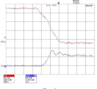
Fig. 5 shows the switching behavior of JFET with switching frequency of approximately 60 kHz. There is a current spike during turn on caused by the booster SiC diode capacitive charge. Current spike can also be reduced by the application of a ferrite bead in the gate circuit. Results are shown in Fig. 6. This is also effective against gate ringing current, however its consequences are slower switching speed and additional switching losses.
Fig. 5a shows a turn on and a turn off transition at app. 50% duty cycle with boosted voltage of 550 VDC and load current of 13 A. In Fig. 5b and 5c an enlarged single period of turn on and turn off can be seen. In this case the gate does not contain a ferrite bead.
Figure 5a
CH1 Cascade voltage, CH2 Cascade Drain current
Figure 5b
CH1 Cascade voltage, CH2 Cascade Drain current
Figure 5c
CH1Cascade voltage, CH2 Cascade Drain current
Fig. 6 shows similar operation conditions that Fig. 5, but the gate contains a ferrite bead.
Figure 6a
CH1 Cascade voltage, CH2 Cascade Drain current (100 mV/A)
Figure 6b
CH1 Cascade voltage, CH3 Cascade Drain current (100mV/A)
5.3 H-Bridge Unit Operation
There is a dangerous effect in the phase legs during on state of the top JFET device. The bottom JFET can have a parasitic turn on due to the miller effect.
It is advisable to apply a negative gate-source voltage to keep the JFET in the turned off state. Aforementioned sensitivity can be further decreased by means of parallel connected gate capacitor of few nF. The experimental H-bridge was not sensitive to those voltage stresses. Fig. 7 shows current and voltage of the top semiconductor.
Figure 7
CH1Cascade voltage, CH2 Cascade Drain current (20 mV/A)
A half sinusoidal output current of the inverter is recorded in Fig. 8, where the switching frequency was 30 kHz. In the same figure the output modulated voltage was recorded in blue. Enlarged signals can be seen at the bottom of Fig. 8b.
Figure 8a
Output current and output voltage of the inverter
Figure 8b
Half sinusoidal output current 500 VDC (500 V/DIV) voltage and 20 A (13.33 A/DIV) load current, modulation frequency 30 kHz
Conclusions
This paper focuses on the application of a new semiconductor class in low power PV inverters. In addition it introduces various solutions and some key rules for circuit design and construction.
The paper points out the advantages and disadvantages of normally on and off JFETs. Furthermore, it presents the measurement results of an experimental PV inverter.
Acknowledgement
This work was supported by Hyundai Technologies Center Hungary Ltd.
References
[1] A. Ritenout, V. Bondarenko, R. Kelley and D. C. Sheridan: Electrical Characterization of Large Area 800V Enhancement- Mode SiC VJFET for High Temperature, Material Science Forum, March 2009, pp. 715-718 [2] R. Kelley and M. S. Mazzola: SiC JFET Gate Driver Design for Use in
DC/DC, APEC ’06, March 2006, pp. 179-182
[3] B. Burger, B. Goeldi, Dirk Kranzer and Heribert Scmidt: 98.5% Inverter Efficiency with SiC MOSFETs in 23rd EU PVSEC, Valencia, Spain, 1st to 4th September 2008
[4] D. Domes, X. Zhang: Cascade Light Normally on JFET Standalone Performance in Normally off Cascade Ciruit. PCIM Europe, 2010
[5] K. Mino, S. Herold and J. W. Kolar: A Gate Drive Circuit for Silicon Carbide JFET, IECON ’03, Nov. 2003, pp. 1162-1166
[6] H. Zhang, L. M. Tolbert: Efficiency of SiC JFET-based Inverters, 4th ICIEA, May 2009, pp. 2056-2059