Future circular collider injection and extraction kicker topologies and solid state generators
M. J. Barnes, W. Bartmann, F. Burkart, L. Ducimeti`ere, B. Goddard, T. Kramer, V. Senaj, T. Stadlbauer, and D. Woog
CERN, Geneva, Switzerland
D. Barna
Wigner Research Centre for Physics, Budapest, Hungary
L. M. Redondo
Lisbon Engineering Superior Institute, GIAAPP/ISEL, Portugal
A. Kandratsyeu
EnergyPulse Systems, EPS, Lisbon, Portugal
(Received 11 March 2019; published 2 July 2019)
A 100 TeV center-of-mass energy frontier proton collider, in a new tunnel of 80–100 km circumference, is a central part of CERN’s Future Circular Colliders (FCC) design study. The designs of the injection and extraction systems of the FCC are initially based upon the parameters of the injection and extraction systems of the Large Hadron Collider and a preliminary study of the FCC beam optics and lattice. The injection and, in particular, the extraction systems of the FCC have to be highly reliable. In order to achieve high reliability, solid state switches will be used for the generators of the injection and extraction systems.
This paper discusses topologies of these kicker systems, which are presently under consideration.
DOI:10.1103/PhysRevAccelBeams.22.071001
I. INTRODUCTION
Line-type modulators, for example, pulse forming lines (PFLs) and pulse forming networks (PFNs), are currently used in many pulse power systems at CERN. These modulators are used to feed klystrons and kicker magnets in the Large Hadron Collider (LHC) and its injectors[1,2].
Line-type topologies include at least one closing high- voltage switch, which can be a spark gap, thyratron, or thyristor [3]: A second closing switch can be used to control the pulse duration in the load. The advantages of the line-type modulators are that they are, in general, relatively simple to design and build, with limited stored energy and good efficiency[3]. Typically, for fast kicker systems, the impedance of the modulator and kicker magnet is matched to avoid reflections; However, this requires that the modu- lator voltage is twice the magnet voltage. The simplest configuration for a pulse forming circuit is a coaxial cable PFL charged to twice the required pulse voltage. The PFL gives fast and low ripple pulses, but low attenuation is
essential, especially with longer pulses, to limit droop and
“cable tail” [4] due to frequency-dependent dispersion in cables.
For machine protection reasons, the pulse duration of the injection kickers, foreseen for the Future Circular Collider (FCC), is only2.0μs (TableI). The injection systems will require relatively fast field rise times, on the order of 430 ns, with a flattop duration of∼2.0μs and a total kick strength of∼2.0T m [5]. This rise time and kick strength are more challenging than for the existing LHC injection kicker systems.
The kicker magnets foreseen for the FCC injection are fast transmission line-type kicker magnets similar to the ones used in the LHC. In order to limit beam-induced heating, the kicker magnets will require a beam screen[6]. Studies have been carried out to characterize the electromagnetic proper- ties of appropriate ferrites[9], which would be used for the yoke and optimize the design of the beam screen[10]. Each injection kicker magnet will have a characteristic impedance of6.25Ω[6,7]. To avoid an excessive overall length for the FCC injection kicker magnets, a high current is desirable.
A current of 2.4 kA would be needed, assuming a magnetic length of 36 m[6], which leads to a required output voltage of the pulse generator of 15 kV[7].
To achieve a high current and fast rise time, high voltage is required. Historically, thyratrons are used to switch the Published by the American Physical Society under the terms of
the Creative Commons Attribution 4.0 International license.
Further distribution of this work must maintain attribution to the author(s) and the published article’s title, journal citation, and DOI.
high voltage and high current with the required, fast, current rise time. However, a thyratron switch is susceptible to an erratic (uncontrolled) turn-on, which could result in the circulating beam being miskicked and, hence, cause considerable damage to accelerator components. In accel- erators such as the LHC, the PFNs are rapidly charged starting a few milliseconds before the injection kickers are required: This keeps to a reasonable minimum the time for which high voltage is across the thyratrons [4].
Nevertheless, erratic turn-ons of the thyratrons still do, occasionally, occur.
One of the major challenges for such a high-energy collider will be the beam dump system, which will have to reliably abort proton beams for each ring, with stored energies in the range of 8.5 GJ: This is more than an order of magnitude higher than for the HL-LHC. The transverse proton beam energy densities are even more extreme, a factor of 100 above that of the presently operating LHC.
For a clean and safe extraction process, the kicker system needs to be exactly synchronized with a particle-free abort gap. The erratic turn-on behavior of thyratron switches does not comply with this requirement and would lead to asynchronous dump events. While asynchronous extraction failures are already a major safety challenge for the LHC [11,12], minimizing or eliminating these is an important requirement, for the FCC, in order to reduce the possibility for such failure modes to the lowest possible. Therefore, the employment of thyratron switches is also excluded for all FCC extraction systems.
The extraction system comprises the extraction kickers, magnetic septa, dilution kickers, and several kilometers of dump line. Those systems must be ready to be used at any time when there is a beam circulating in the FCC. Thus, there will be high voltage on the associated switches, whenever a beam is present, which imposes an additional stress on the switches. The system requirements presently require a fast field rise time of∼1μs and a flattop of at least 326μs (TableI). As the beam will be dumped anyway, the flattop tolerance (5%) is less demanding than for injec- tion and limited only by beam line acceptance and possible dilution pattern constraints.
II. INJECTION SYSTEM
The injection system foreseen for the FCC will require relatively fast field rise times, of not more than 430 ns, with a flattop duration of ∼2.0 μs and a kick strength of
∼2.0T m. This rise time and kick strength are more challenging than for the existing LHC injection kicker systems. The pulse generator for the injection of the 3.3 TeV beam should have a current rise time of
<75ns, to allow a reasonable magnet filling time. For the field flattop duration of ∼2.0μs, a generator pulse duration of∼2.4μs is required. As mentioned above, solid state switches will be used to ensure reliability: The most appropriate switches, in order to achieve fast rise and fall times, are metal-oxide-semiconductor field-effect transistors (MOSFETs).
Solid state modulators differ from the line-type modu- lators by having a switch that can be opened when conducting a full load current, and, therefore, only a portion of the stored energy is delivered to the load during the pulse. Solid state modulator topologies provide a possibility to modify the pulse duration and, thus, to reach high efficiency, because the pulse form can be close to an ideal rectangular pulse with very short rise and fall times.
Solid state modulators provide many advantages over line- type modulators, and especially over single-switch-based modulators. Modulators using thyratrons or spark gaps have limitations with regard to combinations of desired repetition rate, efficiency, pulse width agility, dynamic range, average power, and cost, and in some cases even switch availability[13]. In general, solid state modulators may provide better overall reliability and efficiency and a longer expected lifetime over thyratron-based modulators [13]. The source impedance of a solid state modulator can be low, and hence, unlike a PFL or PFN, the source voltage does not need to be significantly higher than the load voltage. Other key benefits of solid state modulators include the following. (i) The modulator can be built from multiple, identical, lower-voltage modules. Thus, redun- dancy can be built into the system. In addition, the system is readily scalable to higher voltages. (ii) Since the modulator utilizes both an opening and closing switch, the PFL or PFN can be replaced by discrete capacitors.
The relatively short current pulse duration, ∼2.4 μs, is compatible with either an inductive adder (IA) type gen- erator or a Marx generator: Both these topologies will be discussed, for the FCC injection system, in this paper.
A. Inductive adder
The IA consists of a stack of several 1∶1 transformers (Fig. 1). Pulse capacitors, mounted on printed circuit boards (PCBs), are discharged through semiconductor (SC) switches in the primary winding (Fig. 2). Parallel branches are used on the primary side to switch the required output current: The current per branch is limited by the TABLE I. Injection and extraction kicker requirements for the
FCC[6–8].
Parameter Injection Extraction
Kinetic energy [TeV] 3.3 50
Deflection [mrad] 0.18 0.045
Pulse flattop duration [μs] 2.0 ≥326
Flattop tolerance [%] 0.5 ∼5
Field rise time (0.5%–99.5%) [μs] 0.430 1
System impedance [Ω] 6.25
Magnet voltage [kV] 3–15
Magnet current [kA] 0.5–2.4 0.25–4
Repetition rate [Hz] ≤10 <0.05
maximum pulse current capability of the SC switch and/or capacitor. The relatively low system impedance of6.25Ω requires low resistance and parasitic inductance in the primary circuits. To keep the parasitic inductance as small as possible, the primary winding completely encloses the transformer core, and image current planes are close to the primary go conductors. To achieve a low resistance in the primary circuit, SiC MOSFETs with low on-state resistance are proposed [14].
The secondary winding (stalk) of the IA passes through the geometrical center of all transformer cores (Fig.1). In this way, the magnetic flux of every transformer core encloses the secondary circuit loop. The cylindrical design formed by the primary and secondary windings strongly influences parameters such as output impedanceZIA and pulse propagation timetp;IA:
ZIA ¼
ffiffiffiffiffiffiffiffiffiffiffiffiffiffiffiffiffiffiffiffiffiffi LpþLlayer
Clayer
s
; ð1Þ
tp;IAðone wayÞ¼n·
ffiffiffiffiffiffiffiffiffiffiffiffiffiffiffiffiffiffiffiffiffiffiffiffiffiffiffiffiffiffiffiffiffiffiffiffiffiffiffi ðLpþLlayerÞ·Clayer
q ð2Þ
where Lp is the primary circuit parasitic inductance, per layer, which is dependent upon the design of the primary circuit and the number of parallel branches. A typical value for this inductance is∼5nH [16]; Llayer is the secondary inductance of a layer;Clayeris the capacitance between the primary and secondary of a layer.
LlayerandClayerare dependent upon the ratio of the inner diameter (di) of the transformer core housing to the outer diameter (do) of the stalk:
Llayer¼μ0·l· lnddi
2π o; ð3Þ
Clayer¼2πμε0εrl lnddi
o
; ð4Þ
wherelis the height (length) of one layer,μois permeabil- ity of free space (a nonmagnetic insulation is used between the transformer core housing and the secondary winding), εo is the permittivity of free space, and εr is the relative permittivity of the dielectric.
Typically, one end of the IA is directly grounded (Fig.2).
In this case, the output pulse current rise time includes twice the pulse propagation time of the pulse through the stack, since the pulse is reflected from the grounded end of the IA and has to propagate the entire length of the stack a second time[3].
The number of layers defines the maximum output voltage, and the number of parallel branches, on the primary side of the transformer, defines the maximum available output current. Major components of the IA are the SC switches, pulse capacitors, magnetic cores, and high-voltage freewheeling diodes (Fig.2) [13,17].
Advantages of the IA, compared with conventional thyratron based systems, are[13,17](i) all primary circuits are referenced to the ground—high voltage occurs only at the output—and (ii) reduction of droop and ripple of the output pulse is possible by using modulation layers.
Because of saturation effects of the magnetic core, the maximum pulse duration is typically limited to approx- imately3μs: This depends on the voltage per layer, the FIG. 1. Schematic illustration of two inductive adder layers.
FIG. 2. Simplified schematic of an inductive adder [15].
magnetic properties of the core, and the core cross-sectional area (Ac in Fig.1). The modular design of the IA makes it easy to design the device with built-in redundancy.
Additional layers can, for example, compensate a failure in another layer by implementing a logic which either coordinates the usage of the appropriate number of func- tional layers or, alternatively, uses the remaining functional layers but with a slightly increased voltage per layer. The second option allows the nominal voltage per layer to be reduced, and, hence, the lifetime and reliability can be improved.
1. Insulation material
An important aspect of the IA is the insulation material between the primary and secondary transformer windings.
The maximum permissible electric field strength Emax
influences the dimensions of the insulation [Eq.(5)] and, thus, of the diameters of the windings: In addition, the relative permittivity (εr) influences the output impedance [Eqs. (1), (3), and (4)]. Assuming that the insulation is a single material and has a constant relative permittivity, the maximum electric field strength is given by
Emax¼ Vout do
2· lnddi
o
: ð5Þ
Several materials have been considered for the insula- tion: air, oil, water, FC-77, and epoxy. Air would lead to diameters for the magnetic cores in the range of>1.5m:
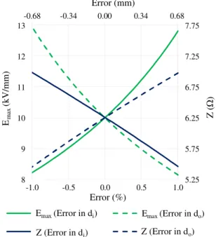
Thus, the cores would be prohibitively expensive. Of the materials considered, oil is the most suitable candidate in terms of the required system impedance, core dimensions, current rise time, cost, and practicability. The breakdown strength of suitable oils is in the range of20kV=mm; thus, 10kV=mm is taken here as a safe operating limit. Figure3 shows the intersection point of the graphs describing the
inner diameters of the transformer core housing and the outer diameter of the stalk, for an electric field of 10kV=mm and a characteristic impedance of 6.25Ω, for an oil with a relative permittivity of 2.7 and an output voltage of 15 kV. The minimum outside diameter for the stalk is 6.8 cm, which results in an oil insulation thickness of only 1.5 mm. The area below the blue curve, in Fig.3, corresponds to a maximum electric field greater than 10kV=mm, whereas the area above the blue curve corre- sponds to a maximum electric field below10kV=mm and, thus, would also be safe for operation.
Figure4shows the influence of a manufacturing error, in either the inner diameter of the primary winding or the outer diameter of the stalk, upon the characteristic imped- ance and the maximum electrical field. It is desirable that Emaxis no more than10kV=mm: Hence, the design could be for a lower electric field and/or the manufacturing tolerances appropriately specified, e.g., þ0, −X mm for the outer stalk diameterdoandþ0,þX mm for the inner core housing diameterdi. It is considered feasible to readily machine the stalk and core housing with a tolerance better than 0.1 mm. As a worst case, consider a−0.1mm (0.15%) error in the outside diameter of the stalk, with respect to nominal: This reduces the maximum electric field from 10 to9.7kV=mm (∼3%) and increases the output impedance from 6.25Ω to ∼6.36Ω (∼1.8%). The influence of this impedance mismatch is being investigated.
To provide compatibility with the Compact LInear Collider (CLIC) prototype IA, so that this prototype can also be used for FCC research and development, a stalk diameter of 10.4 cm has been chosen, resulting in an
10 kV/mm limit
Intersection Prototype insulation
ZIA=6.25 Ω
0.00 0.05 0.10 0.15 0.20
0 0.05 0.1 0.15 0.2
di(m)
do(m) 0.070 0.071 0.072
0.067 0.068 0.069
FIG. 3. Dimensions for oil as an insulation material, for an output voltage of 15 kV, for an electric field of10kV=mm and a characteristic impedance of6.25 Ω.
-0.68 -0.34 0.00 0.34 0.68
5.25 5.75 6.25 6.75 7.25 7.75
8 9 10 11 12 13
-1.0 -0.5 0.0 0.5 1.0
Error (mm)
Z ()
Emax(kV/mm)
Error (%)
Emax (Error in Di) E_max (Error in Do)
Z (Error in Di) Z (Error in Do)
Emax(Error in di) Emax(Error in do) Z (Error in di) Z (Error in do)
FIG. 4. Influence of a manufacturing error, in either the inner diameter of the primary winding or the outer diameter of the stalk, uponEmax and Z.
insulation gap of 2.3 mm for a system impedance of 6.25Ω. The maximum electric field is ∼10kV=mm, for an output voltage of 15 kV and nominal dimensions of the transformer core and stalk. During assembly, particular attention will be paid to ensure that the stalk and core housing are as concentric as possible, to minimize the increase in field strength with respect to nominal. A maximum concentricity error of0.1mm is expected.
2. Semiconductor switches
The SC switches for the IA need to have fast switching times, low on-state resistance, and both high current and voltage ratings. Fast switching is required to achieve the
∼75ns output current rise and fall times. A low on-state resistance is needed, given the low output impedance of the IA, to ensure only a small voltage drop over the MOSFETs:
A high voltage drop would reduce the output voltage as well as increasing the voltage droop[18]—the magnitude of this voltage droop is also dependent upon the magnet- izing inductance of the core.
The higher the voltage and current ratings of the MOSFETs, the lower will be the required number of layers and parallel branches per layer, respectively. A reduced number of layers can decrease the total propagation delay through the IA and, thus, for a given MOSFET switching speed, decrease the output current pulse rise time. In addition, the complexity and costs of the IA are reduced.
Modern SiC MOSFETs are the most promising family of currently available SC switches. Voltages of up to 1700 V and peak pulse currents of more than 100 A, with a switching time less than 10 ns (10%–90%), are feasible.
As this“wide band gap”technology is rather new, further development can be expected. In the case where the IA is used in the tunnel, to minimize the lengths of cables, the radiation hardness of the SiC MOSFETs, and other components, is also of importance.
3. Pulse capacitors
The parasitic inductance of the primary loops, Lp, influences the output impedance of the IA [Eq. (1)].
To reduce Lp, it is important to minimize the capacitor inductance, as it is a significant contributor toLp. Hence, the pulse capacitors used in the IA must have very low parasitic inductance and suitable voltage and current ratings. To guarantee long lifetimes, the charging voltage should be such as to ensure a reasonable electric stress on the dielectric material. For the FCC IA, assuming 24 parallel branches and no droop compensation, a capaci- tance of 52μF per branch and a repetitive peak current rating of at least 110 A per branch are needed. A possibility to reduce the required capacitance is to use analogue modulation: One or more additional layers in the stack serve as modulation layer(s)[17]. In a modulation layer, the primary circuit is replaced by a resistor (passive analogue
modulation) or a parallel circuit consisting of a resistor and a MOSFET (active analogue modulation). The primary circuit of the analogue modulation layer is effectively in series with the load[19]. The voltage across the load is then given by the sum of the voltage generated by the constant voltage layers, minus the voltage across the analogue modulation layer. At the beginning of the pulse, the current in the modulation layer flows through the modulation resistance, generating a voltage drop. During the pulse, the current in the magnetizing inductance of the magnetic core of the modulation layer increases, reducing the current through the parallel resistance. This leads to a reduction of the voltage across the modulation layer[20,21]; hence, the droop of the constant voltage layers can be compensated.
In the case of an active analogue modulation layer, the resistance of the MOSFET is in parallel with the resistor, and, thus, the effective resistance of the layer can be modulated. If the MOSFET is used in its linear region, a ripple on the output voltage can be compensated, too [20,21]. Since the requirement of a combined ripple and droop of0.5% is challenging, it may be necessary to use one or more modulation layers to meet the requirements [17]: Pulses with a stability of0.02% have been reached with this technique at 10.2 kV output voltage[16,22].
Preliminary simulations show that adding a passive analogue modulation layer with a1Ωmodulation resistor would reduce the required capacitance per branch, from 52μF, to approximately33μF (or less). A drawback of the analogue modulation layer is that it reduces the output voltage, and, hence, either a higher voltage per layer or more constant voltage layers are needed to compensate this effect[17].
The width and height of the capacitor influence the output pulse rise time from the IA: The layer height l should be as small as possible to reducetp;IA[Eqs.(2)–(4)].
However, the minimum height is dependent upon the mechanical dimensions of the capacitor and the transformer core. In addition, the capacitor width can, for given dimen- sions of the PCB, limit the number of parallel branches per layer. Custom-made capacitors for this application were successfully tested under appropriate conditions[7].
4. Magnetic cores
A critical component of the IA, not only from the technical point of view but also in terms of cost, is the magnetic core. In order to achieve relatively low core losses, high relative permeability, and a large flux swing, a nanocrystalline, tape-wound, core will be used. For the required pulse parameters, a core cross-sectional areaAcof 25cm2per layer is required: This assumes a layer voltage of approximately 1 kV, a safety factor of 100%, a saturation flux density of 1 T, and a suitably biased core. As mentioned above, the inner diameter of the core is defined by the system impedance, the output voltage, and the maximum permissible electric field for the insulation
material. Furthermore, the core height will be kept small to reduce the layer height and, hence, the propagation delay and output pulse rise time. However, the layer height is also dependent on the height of the pulse capacitor. The outer diameter of the core is currently limited by production constraints and saturation behavior of the core. To avoid excessive saturation of the inside diameter of the core, it is recommended that the outer diameter of the core should not be bigger than 3 times the inner diameter of the core[3,17].
Packing factors in the range of 68%–75% can be achieved for a nanocrystalline tape-wound core [17].
Important parameters of the magnetic core are the linear flux density swing, saturation flux density (Fig. 5), core losses, and magnetizing inductance[3,17]. To minimize the cross-sectional area and avoid saturation, for the required pulse parameters, the available flux density swing needs to be as high as possible, and biasing will be necessary to use the entire flux density span (ΔB≈2T). The core losses should be low and the magnetizing inductance high to minimize the core loss current and the magnetizing current, respectively, during the pulse. To start at a negative flux density (Fig.5), a high permeability and low coercivity of the core are desirable to reduce the biasing current which would be needed. The high permeability is required up to frequencies of several hundreds of kilohertz. Tests and measurements of cores with various initial permeability’s showed that cores with a“square-shaped”flux density (B) to field strength (H) curve are the most interesting option due to easy of resetting to the negative bias [7,23].
In the case of an excessive pulse duration, for example, due to a too-long switch control signal for the IA, the core can saturate leading to a very high magnetizing current:
In this case, the primary current is limited mainly by the parasitic inductance of the primary winding and the characteristics of the MOSFET switches. In order to avoid the SC switches being destroyed, either the current through
the switches must be limited, e.g., by appropriately con- trolling the gate-source voltage, or the MOSFET switches must be turned off by protection electronics. Further investigations of this fault type are ongoing.
5. High-voltage diodes
The high-voltage diodes in the primary circuits of the IA (Fig.2) conduct the magnetizing current when the SC switch is turned off at the end of a pulse: This freewheeling path is needed to avoid an overvoltage breakdown of the MOSFET switches. In addition, in the case of a fault in which one layer does not turn on, the diodes offer a path for the load current to bypass the faulty layer, and, hence, the output voltage is reduced only by the missing voltage of this layer.
6. Prototype construction and challenges Component samples have been ordered for characteri- zation: Tests and measurements were carried out, resulting in the final component selection [7,23]. A small-scale prototype of ten layers was built in 2018 (Fig.7) to prove the feasibility of achieving the required output pulse duration, low ripple, and fast rise time: Initial measurement results are promising, as shown in Fig.6.
The measured leading edge time of 94 ns can be decreased significantly if additional branches are added in the primary to reduce the primary circuit inductance.
Because of the low current capability of the primary circuit (only two branches were installed per layer), measurements have so far been carried out only with a 50Ω load. An analogue modulation layer was not used for the measure- ments shown in Fig.6—the measured droop is 1.7% over an elapsed time of 1.7μs. This droop is approximately twice as large as would be expected: The reason for the discrepancy is being investigated.
Once all measurements on the small-scale prototype are satisfactorily completed, a 22-layer prototype will be built and tested. To date, the prototype IA has been reliable.
However, one concern in terms of the reliability of the IA is
Linear Region
FIG. 5. TypicalB-Hcurve of a nanocrystalline material.Bris the remnant flux-density andBsatis the saturation flux-density of the material.
-12 -10 -8 -6 -4 -2 0
0.0 0.5 1.0 1.5 2.0 2.5
t in µs Voutin kV tr= 94 ns
tf= 107 ns
FIG. 6. Measured output voltage pulse, for the ten-layer small- scale prototype with two branches per layer, across a50Ωload.
the MOSFET switches: These generally fail to short-circuit.
If this occurs in the IA, since the dc power supply is connected across the drain source of the MOSFETs in each layer, this can significantly reduce the output voltage of the power supply, affecting all cells. Similarly, a failure of the dc power supply, if only a single supply is used, will result in the pulse capacitors no longer being charged—thus, their voltage will decay to 0 V. Means of mitigating such failure modes are under study.
The design of the IA prototype for FCC injection will be based on the design of the prototype IA for the CLIC damping ring kicker systems [16–18]. The components can be tested with existing test equipment; However, the mechanical design needs to be adapted to the voltage, current, pulse rise and flattop duration, and impedance and for using oil insulation.
Challenges will include the realization of the small insulation gap, between primary and secondary windings, as well as the fast rise time and relatively long flattop duration. The small insulation gap, of only a few milli- meters, requires a precise production of the hardware components as well as an accurate placement of the stalk through the center of the primary windings. In the case where the insulation gap is not symmetric, around the primary, there could be breakdowns of the insulation. It is preferable that the whole inductive adder is not immersed in the insulation oil: This improves ease of testing and mea- surements, as well as maintenance of the IA. However, oil is required between primary and secondary windings; hence, the design must prevent oil leakage: The best way of achieving this is presently being studied. As a further option, the development of a radiation hard IA is envisaged.
Measurements regarding single-event burnout of state of the art SiC MOSFETs are ongoing.
B. Marx generator
In a Marx generator,ncapacitors are charged in parallel (Fig.8) from a relatively low-voltage dc power supply,Udc, and discharged in series into the load, an idea developed by Erwin Marx in 1923. Hence, the output voltage has an amplitude approximately equal to the input voltage times the number of cells (n), v¼nUdc. In the original Marx generator, spark gaps were used to connect the cell capacitors in series, and a resistor and inductors were used to limit the charging current and self-discharge paths[24].
With the improvement in solid state switch characteristics, major progress has been made in the development of Marx generator–type topologies based on semiconductors [25–30].
The simplest pulse shape that a Marx generator can produce, with a resistive load, is anRCdecay: In this case, the capacitance of the erected Marx discharges into the resistive load. The advantage of using the Marx topology, rather than a single capacitor at a high voltage, is that the maximum voltage across components in a Marx cell is the input power supply voltage,Udc. Therefore, relatively low- voltage components can be used: Since each cell comprises low-voltage components, it is relatively easy to minimize parasitic inductance through the use of closely coupled image planes[25]. In addition, high voltage exists in the Marx generator only when the Marx is erected to produce an output pulse. Also, the energy inside the Marx is stored in several capacitors, instead of one, which has advantages in terms of cost and safety.
Figure 8 shows a simplified circuit of a modern solid state Marx generator[31,32]. One advantage of the Marx generator over the inductive adder is that the Marx does not require magnetic cores to directly generate the output pulse.
Hence, there is the possibility to generate longer-duration pulses, provided that the energy stored in the capacitors of the Marx is sufficiently large—this is also dependent upon the load impedance and the permissible droop of the output pulse.
The basic Marx (Fig. 8) comprises an energy-storing capacitorCi(“i”is an integer in the schematic), two set of diodesDai andDbi, and a half-bridge with two MOSFET switches. MOSFETs labeled Tpi, at the top of the half- bridge, apply pulses to the load, and the bottom MOSFETs, FIG. 7. Ten-layer small-scale prototype IA for the FCC study.
Load
I I
DC
+
-
Udc
C1
Tp1
Tc1 +
Tp2
Tc2
Da1 Db1
Da2 Db2
Da(n-1) Dan
Db(n-1) Dbn
C2+ C(n-1)+ Cn+
Tp(n-1) Tpn
Tc(n-1) Tcn
0
+
-
V0
FIG. 8. Simplified schematic of a solid state Marx generator.
labeledTci, are for charging capacitorsCibetween pulses and for discharging the load capacitances after the pulse.
CapacitorsCiare charged in parallel from power supply Udcby diodesDaiandDbiand MOSFETsTci: During this period, the load capacitance is discharged to 0 V. The pulse is applied to the load by first turning off MOSFETsTciand then by connecting in series capacitors Ci by turning on MOSFETs Tpi. The diodes Dbi are included for safety reasons, as they limit the discharge of eachCicapacitor into theCiþ1onwards capacitors, reducing the damage, if aCiþ1
capacitor fails.
Similarly to the inductive adder, the Marx generator is modular: Hence, the voltage of the output pulse can be increased by connecting more cells in series. The fact that the cells are nominally identical simplifies maintenance and lowers spare counts [33]. However, it is more difficult to ensure fully redundant operation for the Marx, in com- parison to the IA. Depending upon the device failure mode, the Marx operation can be dramatically affected: (a) Power semiconductors normally fail to short-circuit: If a MOSFET in a half-bridge fails in this way, when the other MOSFETs in the same half-bridge turn on, it short-circuits the cell capacitor and the dc power supply; (b) if one diode in the charging path fails to open-circuit, the subsequent capacitor cells are not charged, severely reducing the output pulse magnitude of the Marx; (c) if a MOSFET switch in the top of the half-bridge fails to open-circuit, then the antiparallel diode in the bottom of the half-bridge will conduct and bypass that cell, losing only one1=n of the output pulse voltage; (d) if a MOSFET switch in the bottom of the half- bridge fails to open-circuit, then the antiparallel diode in the top of the half-bridge will conduct and bypass that cell;
thus, the interpulse voltage will be1=nof the output pulse voltage rather than 0 V.
Introducing more devices to increase redundancy results in increased complexity and potentially decreased reliabil- ity. Hence, an important objective of the Marx research is to understand the limitations and mitigate them in terms of limiting fault propagation and ensuring adequate modu- larity to ease the maintenance.
A potential issue with the Marx generator for powering a kicker magnet is the droop of the output voltage as the capacitors, in each cell, discharge. For long (∼ms) pulse durations, an alternative to increasing the cell capacitance values is droop compensation using a buck converter. The buck converter is in series with the main capacitor of each cell of the Marx: The voltage across this capacitor can be controlled by a pulse width modulation (PWM) technique such that the capacitor voltage increases during the pulse—
the sum of the voltage across the buck converter and the main cell capacitor is designed to be constant [30]. This PWM technique is not applicable to the short pulse required for the FCC injection kicker magnets. In Ref.[34], a Marx generator was used to power a kicker magnet at J-Parc:
Staggered turn-on of the cells was utilized to create an
arbitrary waveform. A technique such as staggered turn-on of some cells, whose capacitors are precharged to a lower voltage, may be applicable to correcting output droop of a Marx for the FCC injection kicker: However, this will create a sawtooth waveform. The magnitude of the saw- tooth will depend upon the relative voltage on the two sets of capacitors and the number of cells in the Marx generator.
Alternatively, for short pulse durations, resonant techniques can be applied for pulse voltage droop compensation[35].
Other topologies of the Marx generator also exist: In Ref.[25], switch control power and capacitor recharge power are delivered up the stack of cells through a common-mode choke arrangement rather than using diodes. The common- mode choke arrangement allows the delivery of power to the operating circuitry of each Marx cell without the need for separate isolation transformers. Since the pulse power does not pass through the choke, the size of the core can be optimized considering the value, size, cost, and parasitic capacitance to the ground[25].
Figure9shows a prototype, four-stage, Marx generator developed by ISEL University in conjunction with the company EPS, both of Lisbon, Portugal[36]. This Marx generator is assembled in a coaxial-type structure in order to limit the parasitic inductance. The current flows to the load through the MOSFETs and capacitors, placed around the sides of this structure, and returns back through external, insulated, wires. Each stage operates at a voltage of up to 800 V, and consists of 24 SiC MOSFETs in parallel. The four-stage Marx generator was successfully tested with a load current pulse of 2.7 kA, which meets the specifications for the FCC injection kicker system, into a 1.18Ω resistive load: The measured load voltage pulse is shown in Fig.10. The measured rise and fall times, 10%– 90% of the load voltage, were both approximately 50 ns.
This prototype allows the proposed design to be tested and evaluated, in order to assess the technological advantages of such a system and limitations for the scale up to full voltage.
FIG. 9. Four-stage Marx generator assembled in a coaxial structure (four insulated return conductors per side).
Scaling up this concept requires significant effort, such as separating the main circuit and wires carrying the return current [37]. In addition, modifications to the Marx gen- erator are under consideration so that it can safely limit the current in the event of a short-circuit load (e.g., electrical breakdown in a kicker magnet). Future tests will include long-term stability and reliability, as well as testing under fault conditions.
In summary, a Marx generator is potentially suitable for use as the pulse generator for the FCC injection kickers.
A collaboration agreement has been signed between CERN and ISEL, Portugal, to develop a Marx generator which meets the FCC injection system specifications.
III. EXTRACTION SYSTEM
The extraction kicker system comprises the extraction kickers themselves as well as beam dilution kickers, both of which will be part of the FCC beam dump system and will have to reliably abort proton beams with stored energies in the range of up to 8.5 GJ. The extraction kickers deflect the beam by 0.045 mrad into the extraction septa main field region, which provides an additional kick to completely extract the beam into the dump line. Vertical and horizontal dilution kickers sweep the extracted beam over the dump surface, ideally without any crossing and with optimized beam spacing to distribute the beam energy over the dump core volume[8,38–40]. Both systems have to be precisely synchronized with the particle-free abort gap and have to track the beam energy from injection (3.3 TeV) to flattop (50 TeV). An unsynchronized beam abort or particle in the abort gap would lead to a so-called “asynchronous beam abort.” In this situation, particles are swept over the accelerator surface into the dump channel until the design trajectory is reached. In the LHC, sophisticated protection devices protect the accelerator components; however, in the FCC, an asynchronous dump event would be a catastrophic failure case. The design of protection devices for the planned intensity of 50 TeV is a major challenge and currently limited by material parameters. Hence, a possible design would most likely utilize sacrificial devices. Therefore, the
FCC extraction design aims to avoid situations where sub- stantial particle densities are swept over the machine aperture during extraction. Two key parameters have been identified:
the reliability of the extraction kicker system and the system rise time—the latter defines the amount of beam swept over the aperture in a failure case.
A. Extraction kicker system
In order to reduce the number of erratic turn-ons, the design for the LHC beam dump system excludes thyratron switches. Operational experience of the LHC has shown, however, that the solid state pulse generators are prone to erratic turn-on for several reasons[41,42]. Hence, to ensure adequate redundancy in the LHC system, any circulating beam needs to be dumped once any generator integrity is violated: The protection system can thus trigger the beam dump system if it detects a potential fault. This fault may be due to, for example, single-event burnout of a semiconductor, a high-voltage discharge, or even self-healing of capacitors.
Such events on any of the 30 LHC systems would lead to an asynchronous emergency dump. To mitigate this risk for the FCC extraction, a relatively long length of extraction kicker magnets and a highly segmented system are being consid- ered. The long total length lowers the required current, allowing for reduced voltages—hence, increased reliability.
In addition, a highly segmented system allows the number of modules to be chosen such that an erratic turn-on of a module would not deflect the beam by more than1.5σ. Hence, in this case, the dump action can be delayed to allow for synchro- nization with the abort gap[8,40].
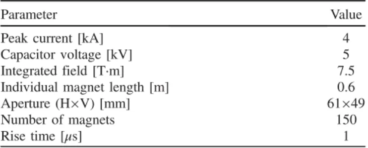
Table II shows the preliminary parameters for such an extraction kicker system. The number of 150 magnets was calculated such that the1.5σoscillation limit is respected and also provides a sufficient margin for installation of up to ten spare modules. Each 600-mm-long magnet module has an aperture of61mm ×49mm: These dimensions allow space for an alumina beam vacuum chamber. Each magnet is powered by an LHC-like solid state generator[43]with a peak current and voltage of only 4 kA and 5 kV, respectively [8,40]. A low inductance of the single turn magnet allows one to achieve a1μs field rise time, which is also essential in terms of the feasibility of protection devices.
For the LHC extraction system, each generator contains two parallel branches, each rated for a full load current.
0.0 0.5 1.0 1.5 2.0 2.5 3.0 3.5
0.0 0.5 1.0 1.5 2.0 2.5
Load Voltage (kV)
Elapsed Time (µs)
FIG. 10. Measured load voltage pulse for four Marx stages (precharge¼800V=stage) into a1.18Ωresistive load.
TABLE II. Extraction kicker magnet parameters for 50 TeV[40].
Parameter Value
Peak current [kA] 4
Capacitor voltage [kV] 5
Integrated field [T·m] 7.5
Individual magnet length [m] 0.6
Aperture (H×V) [mm] 61×49
Number of magnets 150
Rise time [μs] 1
This ensures that, in the event that the switches in one branch fail to turn on, the parallel branch provides the required current. The 150 modules for FCC extraction include ten spares. Hence, a single branch can be used in each FCC extraction generator, greatly simplifying the generator design[43].
A beam screen is required, since the circulating beam passes through the aperture of the extraction kicker magnets. As per the LHC dump system, it is envisaged to provide beam screening by placing an alumina tube in the aperture of the dump magnets. The inner surface of the alumina tube will be coated with a suitable, uniform, thickness (∼2μm) of conductor. However, the alumina tube requires an increase in the aperture of the magnet: The aperture dimensions shown in TableII, for the extraction kicker magnet, include an allowance for the alumina tube.
During the field rise time, eddy currents will be induced in the coating, increasing the field rise time[44]. This will be compensated for by overshooting the field in the dump kicker magnets, which slightly increases the voltage and current for the solid state generators[43].
B. Dilution kicker system
The FCC-hh 50 TeV bunch energy density at the dump absorber has been reviewed, and requirements for a dilution system have been formulated[8,40]. In order to allow for a conventional carbon absorber, a sophisticated dilution kicker system is required. Several dilution patterns have been analyzed and optimized towards a pattern which is reasonably producible by kicker hardware: A spiral will be painted from the outside to the inside of the dump block [18,40,43,45]. This pattern requires a vertical and horizon- tal kicker system oscillating at a frequency of ∼50kHz, with an amplitude decay from 100% to∼50% in350μs.
With a bunch separation of >1.8mm (for 25 ns bunch spacing) and a spiral pitch of>20mm, no trace crossing or bunch overlay occur: A dump block radius in the range of 70–80 cm is required[46].
The dilution system is very technologically challenging.
The basic idea is based on the LHC dilution system but with significant modifications. The feasibility of the FCC dilution is ensured by using a conservative design: It will be a segmented system and comprises a total of 85 outside vacuum magnets, each with a length of 1.5 m [8,40]. A focusing triplet in the dump line is used to reduce the required aperture at the vertical dilution system and, hence, relax the kicker hardware parameters[8]. As per the LHC, lumped inductance magnets will be used, each ∼1.5m long, to give a reasonable inductance per magnet (∼2.3μH to∼2.6 μH). The oscillation frequency will be constant at
∼50kHz (in comparison with 14.2 kHz for the LHC), for a damped sine (H)/cosine (V) wave. No beam screen is required, since the circulating beam does not pass through the aperture of the dilution kicker magnets.
Because of the long sweep path, the high-frequency (f) oscillation is sensitive to frequency mismatches between the vertical and horizontal dilution kicker systems. A maximum frequency mismatch of Δf=f¼0.2% is toler- ated, which results in a temperature increase, of the dump block, of∼100°C compared to the nominal sweep pattern.
The impact of randomly distributed frequency errors of all generators is less critical, and larger errors than Δf=f¼ 0.2% might be acceptable, which is still under study [8].
Segmenting the horizontal and vertical dilution systems into 29 and 56 modules, respectively, has the advantage that the impact of faulty individual modules is not as significant as for a less-segmented system. The vertical system is more challenging due to the large aperture: This situation has already been improved by using a focusing triplet structure in the dump line to reduce the horizontal aperture require- ments for the vertical system[43]. Nevertheless, the maxi- mum current in the vertical dilution system is∼16kA, and a driving voltage of∼19kV is required. The vertical system has to cope with the increasing horizontal aperture: Hence, two vertical magnet types with different apertures have been introduced (TableIII).
Horizontal and vertical systems would use the same generator design which provides the required current and voltage parameters with a 50 kHz sinus oscillation. The vertical system would be triggered5μs after the horizontal one, which is acceptable for scheduled dumps (as the horizontal system can be triggered5μs before the extrac- tion kickers). However, this will be an issue in the event of an asynchronous dump, since the beam would be painted on the horizontal axis before the spiraling starts after5μs.
The resulting crossings, on the dump, of the beam are a potential issue for the dump material, and, hence, this situation is being further studied.
IV. CONCLUSIONS
First considerations for the FCC-hh injection and extrac- tion systems have been made based on the present optics requirements. To achieve the fast rise and fall times and TABLE III. Dilution kicker magnet parameters [8,40], with a triplet.
Parameter Horizontal Vertical
Deflection (mrad) 0.13 0.25
Integrated field (T·m) 22 42
Rise time [μs] 5 5
Magnetic length [m] 43.5 83.5
Gap height [mm] 30 34=40
Gap width [mm] 30 40=46
Inductance [μH] 2.3 2.6
Current [kA] 12 16
Voltage [kV] 12 19
Number of magnets 29 56
Oscillation frequency [kHz] 50 50
flattop duration, for the injection kicker system, solid state generators based on both the inductive adder and Marx generator concepts have been presented: Both concepts appear to be feasible. Advantages and disadvantages of the Marx, with respect to the IA, have been discussed. In order to prove the principle and to test the performance, a prototype inductive adder has been built at CERN using a nanocrystalline core and SiC MOSFET switches.
Furthermore, a Marx generator prototype has also been developed by ISEL, Portugal, and is the subject of an ongoing collaboration agreement.
For the beam dump system, a segmented extraction kicker concept has been developed together with a dilution kicker system to achieve an optimized dump pattern. The segmented extraction kicker system has several advantages:
Short magnets will keep the inductance low, which allows for fast rise times, and the subsequently high number of modules will keep the required kick strength per module low. Thus, a prefire of one module would lead only to a circulating beam oscillation of1.5σ, which would not result in an asynchronous dump of the beam. The individual module parameters seem feasible and will allow the requirements to be achieved using solid state switches.
The dilution kicker system still needs to be optimized;
However, the basic concept of horizontal and vertical kicker magnets powered by solid state generators delivering a sinus oscillation is considered feasible. An optimized dump pattern has been studied: Considering the dump block material parameters, no trace crossings are allowed for nominal operations—hence, a spiral is the optimum pattern to be painted onto the dump block.
Further studies will be needed for both injection and extraction systems to develop detailed solutions and to adapt to changing design parameters.
[1] The LHC Main Ring, LHC Design Report Vol.I, edited by O. S. Brüning et al. (CERN, Geneva, 2004), https://cds .cern.ch/record/782076.
[2] The LHC Injector Chain, LHC Design Report Vol. III, edited by M. Benedikt et al. (CERN, Geneva, 2004), https://cds.cern.ch/record/823808.
[3] Induction Accelerators, edited by K. Takayama and R. J.
Briggs (Springer, New York, 2011), ISBN: 978-3-642- 13916-1.
[4] M. J. Barnes, Kicker systems, CERN Yellow Reports, 2018,https://doi.org/10.23730/CYRSP-2018-005.229.
[5] E. Renner et al., Design and Evaluation of FCC-hh Injection Protection Schemes, inProceedings of IPAC’18, Vancouver, BC, Canada (JACoW Publishing, Geneva, Switzerland, 2018) pp. 854–857, https://doi.org/10 .18429/JACoW-IPAC2018-TUPAF059.
[6] A. Chmielinska, M. J. Barnes, W. Bartmann, F. Burkart, and B. Goddard, Preliminary estimate of beam induced power deposition in a FCC-hh injection kicker magnet, in
Proceedings of the IPAC’17, Copenhagen, Denmark (JACoW, Geneva, 2017).
[7] D. Woog, M. J. Barnes, L. Ducimeti`ere, J. Holma, and T. Kramer, Design of an inductive adder for the FCC injection kicker pulse generator, in Proceedings of IPAC’17, Copenhagen, Denmark(JACoW, Geneva, 2017).
[8] E. Renner, Machine protection of the Future Circular Hadron Collider FCC-hh: Injection and extraction, M.Sc. diploma thesis, Vienna University of Technology, 2018,http://cds.cern.ch/record/2648770.
[9] A. Chmielinska, M. J. Barnes, F. Caspers, B. K. Popovic, and C. Vollinger, Measurements of electromagnetic proper- ties of ferrites as a function of frequency and temperature, J. Phys. Conf. Ser.1067, 082018 (2018).
[10] A. Chmielinska et al., FCC injection kicker magnet design, impedance and heating aspects, in Proceedings of FCC Week 2018, https://indico.cern.ch/event/656491/
contributions/2947268/.
[11] T. Krameret al., Performance studies for protection against asynchronous dumps in the LHC, in Proceedings of the International Particle Accelerator Conference, Kyoto, Japan(ICR, Kyoto, 2010).
[12] T. Kramer, LHC beam dump system analysis of beam commissioning, performance and the consequences of abnormal operation, doctoral thesis, Graz University of Technology, Graz, Austria 2011,http://cds.cern.ch/record/
1392619?ln=en.
[13] M. J. Barneset al., Inductive adders for replacing thyratron based modulators at CERN, in Proceedings of EPE’15 Geneva Switzerland(2015).
[14] D. Woog, M. J. Barnes, A. Ferrero Colomo, J. Holma, and T. Kramer, First prototype inductive adder for the FCC injection, inProceedings of IPAC’18, Vancouver, Canada (JACoW, Geneva, 2018).
[15] J. Holma and M. J. Barnes, Evaluation of components for the high precision inductive adder for the CLIC damping rings, in Proceedings of the 3rd International Particle Accelerator Conference, New Orleans, LA, 2012(IEEE, Piscataway, NJ, 2012).
[16] J. Holma, M. J. Barnes, and A. Ferrero Colomo, Demon- stration of feasibility of the CLIC damping ring extraction kicker modulators, inProceedings of IPAC’18, Vancouver, Canada(JACoW, Geneva, 2018).
[17] J. Holmaet al., A pulse power modulator with extremely flat-top output pulses for the Compact Linear Collider at CERN, Ph.D. thesis, Aalto University publication series, Doctoral Dissertation 196/2015, Helsinki, Finland, 2015, https://cds.cern.ch/record/2130258.
[18] T. Krameret al., FCC-hh injection and extraction kicker topologies and solid state generators, in Proceedings of FCC Week 2016, Rome, Italy(2016).
[19] E. J. Goweret al., Analog amplitude modulation of a high voltage, solid state inductive adder, pulse generator using MOSFETs, in Proceedings of the International Power Modulator Symposium and High-Voltage Workshop, Hollywood, CA, 2002.
[20] J. Holmaet al., Preliminary design of the pulse generator for the CLIC DR extraction system, inProceedings of the PPC, Chicago, 2011, pp. 1353–1358.
[21] J. Holma and M. J. Barnes, Pulse power modulator devel- opment for the CLIC damping ring kickers, CERN Technical Report No. CLIC-Note-938, 2012, https://cds .cern.ch/record/1448259.
[22] J. Holma, M. J. Barnes, and D. Woog, Measurements on 12.5kV inductive adders with200ppm pulse flatness over 900 ns for CLIC damping ring kickers at CERN, in Proceedings of the 2018 IEEE International Power Modu- lator and High Voltage Conference (IPMHVC), Jackson, 2018.
[23] D. Wooget al., Magnetic core and semiconductor switch characterisation for an inductive adder kicker generator, inProceedings of FCC Week 2017,https://indico.cern.ch/
event/556692/contributions/2604327/.
[24] W. L. Willis, in Pulse-Voltage Circuits, 1st ed., edited by R. E. Dollinger and W. James Sarjeant (Tab Books, New York, 1989), Chap. 3, ISBN: 0-8306-9094-8.
[25] J. A. Casey, F. O. Arntz, M. P. J. Gaudreau, and M.
Kempes, Solid-state Marx bank modulator for the next linear collider, in Proceedings of the Pulsed Power Conference, 2003, pp. 641–644.
[26] A. Krasnykh, R. Akre, S. Gold, and R. Koontz, A solid-state Marx type modulator for driving a TWT, in Proceedings of the 24th International Power Modulator Symposium Norfolk, VA, 2000.
[27] R. Phillips, M. P. J. Gaudreau, M. Kempkes, K. Ostlund, and J. Casey, Affordable, short pulse Marx modulator, in Proceedings of the IEEE International Vacuum Electronics Conference 2013, pp. 455–456.
[28] S. C. Glidden and H. D. Sanders, Solid state Marx gen- erator, inProceedings of the Power Modulator Conference 2006.
[29] T. Beukers, C. Burkhart, M. Kemp, R. Larsen, M. Nguyen, J. Olsen, and T. Tang, P1-Marx modulator for the ILC, in Proceedings of the IEEE Power Modulator and High Voltage Conference 2010, pp. 21–22.
[30] M. A. Kemp, A. Benwell, C. Burkhart, D. MacNair, and M.
Nguyen, The SLAC P2 Marx, inProceedings of the IEEE Power Modulator and High Voltage Conference 2012, pp. 1721–1728.
[31] L. M. Redondo, A. Kandratsyeu, M. J. Barnes, S.
Calatroni, and W. Wuensch, Solid-state Marx generator of the Compact Linear Collider breakdown studies, in Proceedings of the International Power Modulator and High Voltage Conference, San Francisco, 2016,https://doi .org/10.1109/IPMHVC.2016.8012824.
[32] L. M. Redondo and J. Fernando Silva, Repetitive high- voltage solid-state Marx modulator design for various load conditions,IEEE Trans. Plasma Sci.37, 1632 (2009).
[33] M. A. Kemp, Solid state Marx modulators for emerging applications, in Proceedings of the 26th International Linear Accelerator Conference (LINAC12), Tel Aviv, Israel, 2012.
[34] S. Fukuoka, K. Fan, K. Ishii, T. Sugimoto, and J.
Matsumoto, Development of a fast kicker system for
J-Parc main-ring injection, in Proceedings of IPAC’13, Shanghai, China, 2013, pp. 684–686.
[35] H. Canacsinh, L. M. Redondo, J. F. Silva, and B. Borges, Voltage droop compensation based on resonant circuit for generalized high voltage solid-state Marx modulator, in Proceedings of the 2016 IEEE Applied Power Electronics Conference and Exposition (APEC), Long Beach, CA, 2016, pp. 3637–3640,https://doi.org/10.1109/APEC.2016 .7468392.
[36] M. J. Barnes, L. M. Redondo, A. Kandratsyeu, and T.
Fowler, Marx prototype pulse generator design and initial results, inProceedings of FCC Week 2018,https://indico .cern.ch/event/656491/contributions/2947267/.
[37] L. M. Redondo, A. Kandratsyeu, and M. J. Barnes, Marx generator prototype for kicker magnets based on SiC MOSFETs,IEEE Trans. Plasma Sci.46, 3334 (2018).
[38] W. Bartmannet al., Dump system concepts for the Future Circular Collider, Report No. CERN-ACC-2017-0079, 2017.
[39] A. Lechneret al., FCC-hh protection absorbers and dumps, inProceedings of FCC Week 2018,https://indico.cern.ch/
event/656491/contributions/2930779/.
[40] E. Renner et al., Optimization of the FCC-hh beam extraction system regarding failure avoidance and mitiga- tion, in Proccedings of the IPAC’18, Vancouver, BC, Canada (JACoW Publishing, Geneva, Switzerland, 2018), https://doi.org/10.18429/JACoW-IPAC2018-TUPA F058.
[41] R. Filippini and J. Uythoven, Review of the LBDS safety and reliability analysis in the light of the operational experience during the period 2010-2012, Report No. CERN-ATS-Note-2013-042 TECH, 2013,https://cds .cern.ch/record/1566431.
[42] M. A. Fraser et al., Considerations on an upgrade pos- sibility of the LHC beam dump kicker system, inProceed- ings of IPAC’16, Busan, Korea, 2016, pp. 3631–3633.
[43] W. Bartmann, M. J. Barnes, F. Burkart, B. Goddard, T.
Kramer, A. Lechner, N. Magnin, and E. Renner, FCC–hh:
Extraction and dilution kicker,https://indico.cern.ch/event/
656491/contributions/2947271/attachments/1631682/
2601592/Renner_FCC_week_2018_ExtDil_Kicker.pdf.
[44] M. J. Barnes, T. Fowler, M. G. Atanasov, T. Kramer, and T. Stadlbauer, Effect of a metallized chamber upon the field response of a kicker magnet: Simulation results and analytical calculations, in Proceedings of the 3rd International Particle Accelerator Conference, New Orleans, LA, 2012 (IEEE, Piscataway, NJ, 2012), pp. 3686–3688, available athttp://www.JACoW.org.
[45] T. Kramer et al., Considerations for the injection and extraction kicker system of a 100 TeV centre-of-mass FCC-hh collider, in Proceedings of IPAC’16, Busan, Korea (2016).
[46] A. Lechneret al., Dilution requirements for the FCC-hh dump, inProceedings of FCC Week 2018,https://indico .cern.ch/event/656491/contributions/2947272/attachments/
1631698/2601617/2018_12_04_fccdump.pdf.
![FIG. 2. Simplified schematic of an inductive adder [15].](https://thumb-eu.123doks.com/thumbv2/9dokorg/1065436.70569/3.918.93.431.69.313/fig-simplified-schematic-inductive-adder.webp)

![Figure 8 shows a simplified circuit of a modern solid state Marx generator [31,32]. One advantage of the Marx generator over the inductive adder is that the Marx does not require magnetic cores to directly generate the output pulse.](https://thumb-eu.123doks.com/thumbv2/9dokorg/1065436.70569/7.918.102.422.65.386/simplified-generator-advantage-generator-inductive-magnetic-directly-generate.webp)
![Figure 9 shows a prototype, four-stage, Marx generator developed by ISEL University in conjunction with the company EPS, both of Lisbon, Portugal [36]](https://thumb-eu.123doks.com/thumbv2/9dokorg/1065436.70569/8.918.492.822.795.1028/figure-prototype-generator-developed-university-conjunction-company-portugal.webp)