Journal Pre-proofs
Full Length Article
Wetting Properties, Recrystallization Phenomena and Interfacial Reactions between Laser Treated Cu Substrate and SAC305 Solder
József Hlinka, Zsolt Fogarassy, Ágnes Cziráki, Zoltán Weltsch
PII: S0169-4332(19)32943-5
DOI: https://doi.org/10.1016/j.apsusc.2019.144127
Reference: APSUSC 144127
To appear in: Applied Surface Science Received Date: 21 July 2019
Revised Date: 12 September 2019 Accepted Date: 19 September 2019
Please cite this article as: J. Hlinka, Z. Fogarassy, A. Cziráki, Z. Weltsch, Wetting Properties, Recrystallization Phenomena and Interfacial Reactions between Laser Treated Cu Substrate and SAC305 Solder, Applied Surface Science (2019), doi: https://doi.org/10.1016/j.apsusc.2019.144127
This is a PDF file of an article that has undergone enhancements after acceptance, such as the addition of a cover page and metadata, and formatting for readability, but it is not yet the definitive version of record. This version will undergo additional copyediting, typesetting and review before it is published in its final form, but we are providing this version to give early visibility of the article. Please note that, during the production process, errors may be discovered which could affect the content, and all legal disclaimers that apply to the journal pertain.
© 2019 Published by Elsevier B.V.
Wetting Properties, Recrystallization Phenomena and Interfacial Reactions Between Laser Treated Cu Substrate and SAC305 Solder
József Hlinka a, Zsolt Fogarassy b, Ágnes Cziráki c, Zoltán Weltsch a,d
a Budapest University of Technology and Economics, Faculty of Transportation Engineering and Vehicle Engineering, Budapest, Hungary;
H-1111 Budapest, Műegyetem rkp. 3.
b Institute for Technical Physics and Materials Science, Centre for Energy Research, Hungarian Academy of Sciences, Budapest, Hungary;
H-1121 Budapest, Konkoly-Thege Miklós út 29-33.
c Eötvös Loránd University, Department of Materials Physics, Budapest;
H-1117 Budapest, Pázmány Péter sétány 1/a.
d John von Neumann University, GAMF Faculty of Engineering and Computer Science, Kecskemét, Hungary; H-6000 Kecskemét, Izsáki út 10.
email address:
József Hlinka jozsef.hlinka@gjt.bme.hu Fogarassy Zsolt fogarassy@mfa.kfki.hu Cziráki Ágnes a.cziraki@freemail.hu
Zoltán Weltsch weltsch.zoltan@gamf.uni-neumann.hu (corresponding author) Abstract
Effect of laser treatment has been studied on the wetting ability of Cu substrate during soldering with SAC305 solder paste. The contact angle of molten solder drops on Cu substrate changes when the substrates treated with different Nd:YAG laser powers. The correlations between the extraordinary change of wetting angle and the surface interaction between the melt pool of solder alloy and Cu plates are studied. A texture formation was found in the laser treated Cu substrate, which supports the diffusion of the Sn atoms. The thickness of Cu3Sn interface layer is increasing with increasing laser power helping the formation of Cu6Sn5 phase, and resulting a better metallic bonding in solder joints.
Keywords: Cu, Laser treatment, Nd:YAG, SAC solder, Wetting angle
Graphical abstract
1. Introduction
The Sn-Ag-Cu eutectic alloy was found the most promising soldering material as an alternative for the lead-free soldering alloys [1, 2]. During the soldering process, between the Cu substrate and the melt pool of SAC305 solder alloy contact develops leading to chemical interaction along the contact surface. The nature of this interaction depends on many parameters including surface contaminations (mainly the adsorbed oxygen), surface roughness, and surface (local) microstructure.
To improve the surface wettability, in order to achieve good quality solder joints, the removal of oxygen contamination is inevitable from the copper surface. Recently the laser treatment has been proposed and, successfully applied for removing the copper oxide from the surface [3]. Besides the removal of copper oxide, thermal and mechanical effects or surface melting may also include in the ablation mechanism at lower power than those at which cleaning is initialized [4, 5]. Localised surface melting was found to occur even at relatively low power density of laser beam. According to the optical micrographs “wavelike” rings are formed around the spot of laser beam. Such wavelike surface morphology hints to the resolidification of molten surface layer. At higher power, debris began to appear around the edge of craters as a result of ejection of ionised material or plasma-induced shock waves causing explosive material ejection [4]. According to that investigation, the copper oxide was removed successfully, but the question is how the laser spot topography affects surface wettability for soldering.
Microstructure of copper surface layer was studied after laser irradiation [6, 7, 8] and it was found, that columnar crystals formed in the molten pool perpendicular to the surface and new preferential orientation distribution is formed in the vicinity of surface layer as a consequence of temperature gradient in the molten pool. Theoretical calculation also revealed [6, 7, 9, 10]
that surface energy change on the irradiated substrate material regularly depends on the variation of applied laser power, which improve the mutual wettability between the solder alloy and the irradiated copper sheet.
In the present work, after the wettability measurements, the interfacial structure was investigated between the SAC305 solder paste and the laser treated Cu substrate on the cross section of the sample (solder/substrate), in order to understand the wettability changing of the laser treated Cu surface.
2. Experimental
2.1. Sample preparation
The measurements were performed with Senju M705-GRN360-KV Lead free SAC305 solder paste, which consist of Sn96.5Ag3Cu0.5 solder alloy powder. This is a usual commercial soldering paste with a mixture of solder alloy powder and flux. The amount of the used solder paste for a wettability measurement was 90±2 mg.
The wetting angle of solder pastes were examined on Cu ETP R240 (CW004A) copper plates (15x15x1 mm) as substrates. This type of copper is widely used for electrical and electronic applications. Before the measurements the copper plates were grinded and polished to remove the oxide layer and reach similar surface properties in every sample and washed with 96 % ethanol (C2H6O).
2.2. Laser treatments of Cu substrate
The laser used in the study was Rofin DY 027, Nd:YAG pulsed laser with emission of 1064 nm wavelength laser beam. The laser beam was focused directly onto a 0.4 mm diameter spot on the surface of copper plate. During the laser surface treating process, the laser beam was traversed across the copper samples by means of a laser scanner at speed of 500 mm/min.
The laser scanning speed must be controlled properly to ensure that a 40 x 40 mm square area can be treated by laser. Different laser powers, from 100 to 2500 W, were used in this process.
The laser was used in continuous wave. Argon gas was used as shielding gas to protect the samples from oxidation during laser irradiation with the flow-rate of 12.5 l/min.
2.3. Wetting angle measurements
The wetting experiments were performed in a wetting angle measuring system which can measure the wettability using sessile drop method [11], taking the methodological issues summarized by Sobczak [12] into account.
The measurements can be performed in inert (Ar) atmosphere. The heat required for the measurements provided by a resistance-heated tube furnace which can ensure the measuring temperature up to 1473 K [13]. In this paper the measuring temperature was not high, the melting temperature of investigated solder is below 523 K.
At the beginning of the wetting angle measurements the samples were positioned into the furnace at ambient conditions. The temperature was raised up to the measuring temperature.
The contact angle values of the drop were measured directly from its images. The total uncertainty of the measured values was ±1˚.
After the wetting angle measurement, the furnace was switched off and was left to cool to ambient temperature. After that, the furnace was dismounted and the sample was removed.
2.4. Structural characterisation
X ray diffraction measurements (XRD) were used to study the microstructure of the Cu substrates before and after laser treatments applying a Philips X’pert equipment.
For the analyses of the crystal structure transmission electron microscopy (TEM) and scanning electron microscopy (SEM) were applied. TEM studies were carried out in a Philips CM-20, working at 200 keV. The TEM was equipped with a Bruker X-ray detector (EDS). The samples were cross-sectional thinned by ion beam milling for the investigations.
3. Results
3.1. Wetting experiments
In Fig. 1 the contact angle of molten SAC305 alloy drop on Cu substrate is plotted versus the change of laser power applied during the previous surface treatment. It is surprising, that correlation is not monotonic between the quantities. Within the small power (below 400 W) the wettability increasingly deteriorates but this tendency turns to oppose at around 500 W i.e., the wetting is gradually improved and reaches saturation value. Fig. 1. shows that the contact angle decreased from 25.2 to 19.2°, which indicate that the surface energy increased until the 2500 W Nd:YAG laser irradiation.
Figure 1. Contact angle as function of laser power applied at the Cu substrate treatment 3.2. XRD-measurements
The crystal orientation on the copper surface was examined by X-ray diffraction analysis before and after the laser treatments. In Fig. 2. the relative intensities are presented for different samples.
Comparing the relative intensity data of copper powder with XRD result of untreated Cu surface, the difference clearly shows the preferred orientation of the copper plate is (220) crystal face, which is the consequence of previous rolling process, applied during the sample preparation. At 400 W irradiation the original preferred orientation of the Cu substrate further increases, so the texture development is more pronounced, than before the surface treatment. It means, that local heat treatments associated with the laser irradiation is insufficient to cause local melting in the surface layer. Recrystallization is taking place only, and the preferred orientation growth crystallites is more pronounced resulting the higher relative intensity of (220) reflection. As it is obvious from Fig. 1., that this kind of structural change proceeds in solid state, resulting in increased grain growth which does not promote the wettability on the copper surface. Contrary, the transient increase of wetting angle was observed, which hints to the wettability decrease in this range of pre-treatment. In addition, the intensity of (200) reflection increases compared to the untreated state beyond 500 W irradiation power, showing the increasing number of crystal orientation of <100> crystal direction. This tendency is shown by the diagram in Fig. 2.
Figure 2. Relative intensities detected by XRD measurements on powder Cu sample [14]
(taken from ASTM data system) and the laser treated Cu surface
In agreement with the earlier investigation [7, 9] these power values can already result local melting in the vicinity of copper surface. Consequently, the crystal structure in the surface layer reflects the growing mechanism from molten state in which high temperature gradient exists, due to the intensive unidirectional heat supply. Under such circumstances the preferential growth (highest growing rate) is favoured in the <100> crystal direction during the solidification. The thickness of modified layer is a function of the applied laser power. The rate of solidification is higher at lower power range, the observed anomaly in the wettability can be associated with the direction dependence of relative XRD intensities at 500 W laser power. (See Fig. 1.)
3.3. SEM and TEM analysis
In order to understand the interfacial structures between the drop and the substrate, the cross section of solidified samples was characterized by TEM study after each wetting experiment.
Fig. 3.a shows the cross sectional TEM picture of the untreated sample. The right side of the picture exhibits the microstructure of the untreated Cu substrate which is typical after rolling process in agreement to the XRD investigations. Comparing the microstructure of the Cu substrates treated with different laser powers it can be seen (See Fig. 3.) that the characteristic structure caused by rolling process gradually changes.
Figure 3. Cross sectional bright field TEM picture taken on the interface of the untreated (a), treated with 300 W (b), 500 W (c) and 2500 W (d) laser power Cu substrate and the SAC
solder drop.
At 300 W laser power only a recrystallization takes place, resulting waviness of the Cu surface (See Fig. 3.b). By applying larger laser power, the Cu substrate is melted and then rapidly resolidified during the unidirectional and Cu grains nucleate and grow. The most convenient growing direction is <100> at the Cu surface (See Fig. 3.c) confirming the (100) texture, detected by XRD measurements.
According to the selected area diffraction study was investigated. At the solder-substrate interface the crystal structure of the interface layer corresponds to the Cu3Sn phase. The structural details of the transition Cu3Sn layers are more visible on Fig. 3. depending on laser performance (laser power applied for Cu substrate before soldering). In the transition layer the Cu3Sn crystallites form columnar structure perpendicular to the Cu substrate surface. The average grain size of the Cu3Sn crystallites is the smallest on the Cu substrate irradiated with 300 W laser power among the investigated samples, and the largest in the sample irradiated with 2500 W laser power, where the elongated Cu3Sn crystallites spread out all of the wideness of the interface layer. This sample exhibits the best wetting property among the investigated samples.
Table 1. Thickness of transition layer in function of laser irradiation.
Laser power (W) Average thickness of the transition layer (nm)
0 330
300 370
500 510
2500 400
The thickness of Cu3Sn grains is increasing with increasing laser powers (see Table 1.). At the same time the total thickness of the transition layer is the largest at 500 W laser power, but the SAED (Selected Area Electron Diffraction) studies revealed, that in this case the transition layer consists of two kinds of crystallites forming double layers (See Fig. 4.a). As the dark field picture shown in Fig. 4.b, a new phase appears on the top of the columnar Cu3Sn interface layer.
This thinner (about 100-120 nm) layer consists of small Cu41Sn11 (ASTM 30-0510) crystallites based on their electron diffractions pattern. This phase and this double layered structure were detected only in the sample irradiated with 500 W laser power causing the observed extreme behaviour in wetting properties (See Fig. 1.).
Figure 4. On the a) a Bright-field TEM image of the sample treated by 500W laser power, which exhibits double layered structure of the interface layer. On the b) a Dark-field TEM image taken on the sample treated with 500 W laser power using the reflections of Cu41Sn11
phase.
On the solder side of the transition layer (inside the drop) Cu6Sn5 (ASTM 45-1488) and Cu6,2Sn5 (ASTM 47-1575) phases were detected in all of the investigated samples.
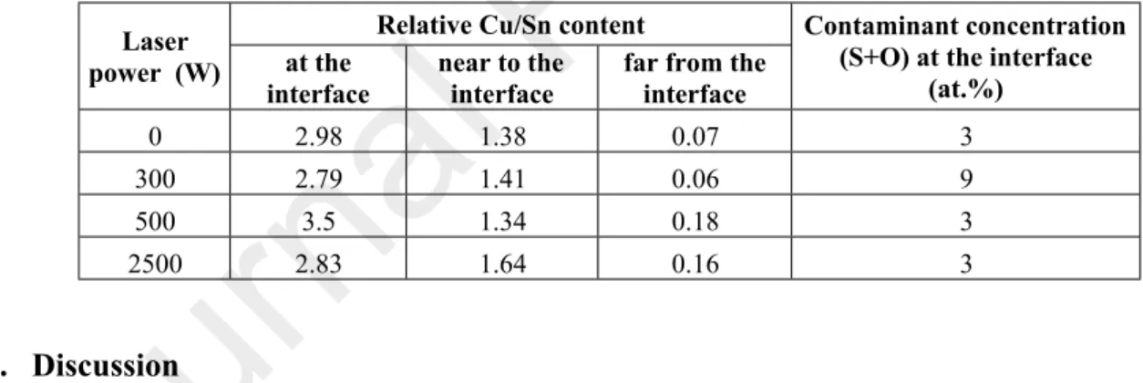
3.4. Results of elements analysis (EDS)
The EDX elemental analyses were performed along the sample cross section confirmed by the results of TEM investigations. Table 2. shows the relative Cu/Sn contents measured at three different points of the SAC305 solder drops. The counted relative Cu/Sn concentrations in the Cu-Sn phases identified by selected area diffraction are the following; (Cu3Sn) 3, (Cu41Sn11) 3.7, (Cu6Sn5) 1.2 and (Cu6.2Sn5) 1.25. As it is collected in Table 2., the relative Cu/Sn concentration is about 3 near to the interface of the Cu substrate and the SAC solder, which corresponds to the Cu3Sn phase detected by SAED. Only exception is the sample treated with 500 W laser power, where 3.5 Cu/Sn relative content was measured. Taking account, the result of TEM this higher value is understandable, because the interface layer consists of a wider Cu3Sn and a thinner Cu44Sn11 phases in this sample according to the TEM study (See Fig. 4.).
Near to the interface the relative Cu contents are between 1.34-1.64 values, which correspond to the (Cu6Sn5) 1.2 and (Cu6.2Sn5) 1.25 phase observed by TEM investigations. Far from the interface (5-10 µm inside the solder drop) the relative Cu content decreases below 0.2 according to the SEM measurements. Remarkable that the Cu content increases slightly inside the solder drop, where the Cu substrate was treated with higher laser power.
The contaminant concentration (S+O) was investigated at the interface with EDS, the results are in Table 2. The contaminant concentration is significantly increasing at sample prepared on the 300 W laser irradiation Cu surface. The other investigated TEM samples contaminant concentration at the interface were similar.
Table 2. Changes of the Cu-Sn contents in the transition layer and inside the drop.
Relative Cu/Sn content Laser
power (W) at the
interface near to the
interface far from the interface
Contaminant concentration (S+O) at the interface
(at.%)
0 2.98 1.38 0.07 3
300 2.79 1.41 0.06 9
500 3.5 1.34 0.18 3
2500 2.83 1.64 0.16 3
4. Discussion
Recent experiments show that the laser treatment over 400 W laser power has been successfully applied to polycrystalline Cu substrate improving the soldering wettability, so better quality of solder joined was achieved. When the energy of laser treatment is less than 400 W, the Cu substrate surface does not melt, only the grain size grows as an effect of heating.
During this grain grow the contaminations diffuse from the grain boundaries to the Cu surface decreasing the wetting ability. Near to 500 W laser power the Cu surface melts and the surface contaminants evaporate clearing the substrate surface and enabling a better wetting. Increasing the laser power the melted volume of Cu substrate increases, and a higher amount of contaminations segregates from the melted volume on the Cu surface. This could be compensated with the effect of the texture formation discussed below. However, we can also assume that after a sufficiently large amount of melted volume the larger part of the contamination will precipitate from the copper solution near to the solid phase, which also increase the wetting.
Metallic bonding in solder joints is achieved by filler alloy, which form Cu-Sn intermetallic compounds of Cu3Sn and Cu6Sn5. Cu3Sn forms a layer on the Cu substrate with a volume diffusion controlled process. Sn atomic diffusivities are different along various crystal orientations of Cu, and the most convenient in <100> direction [14].
In the present work the XRD investigations revealed that the laser treatment of the Cu substrate surface causes recrystallization process. Below 500 W laser power a recrystallization process takes place near to the Cu surface taking more dominant the original (220) texture caused by rolling, which unfavourable for Sn atomic diffusion into the Cu substrate. This is one of the reason next to the surface contamination increase why the soldering wettability is worse, than without laser treatment under 400 W laser treatment. Over 500 W laser irradiation the Cu surface melts, and most of the crystallites resolidified in <100> direction, which is the favourable (lowest activation) crystallographic direction for Sn atomic diffusion, hence promoting the growth of Cu3Sn interface.
According to the present TEM study the thickness of Cu3Sn interface layer increases with the increasing laser power treated preliminary on the Cu surface. The Cu3Sn crystallites form a columnar structure perpendicular to the Cu substrate surface. Their perpendicular grain boundaries act as fast diffusion channels for Cu atoms helping the formation of Cu6Sn5 and Cu6.26Sn5 phases in the solder drop, because the formation of these phases takes place with grain boundary diffusion mechanism. The most clearly visible grain boundary channels were found in the Cu3Sn interface on the Cu surface irradiated with the highest laser power.
Any kind of precipitates with Ag contents were not detected in the interface by TEM investigations, which result confirms the earlier opinions [11]. The Ag atoms do not inhibit the formation of intermetallic compound layers of Cu3Sn and Cu6Sn5. The addition of Ag believed to affects the growth orientation and the coarsening behaviour of Cu6Sn5 grains changing the interfacial energy between the molten solder and interfacial intermetallic compounds.
5. Conclusion
Recent experiments show that the laser treatment over 400 W laser power has been successfully applied on polycrystalline Cu substrate to improve the wettability of SAC305 solder. When the energy of laser treatment is less than 400 W, the surface of the Cu substrate does not melt, only the size of the grains grows as an effect of heating.
Besides of the removal copper oxide from the surface over 500 W of laser treatment, a <100>
texture formation was found in the resolidified surface layer where laser irradiation was investigated. The <100> texture formed during the resolidification of Cu substrate layer is the most convenient for the atomic diffusivities of Sn atoms, helping the growth of Cu3Sn interface.
The thickness of Cu3Sn interface layer thrive with increasing laser power, and their perpendicular grain boundaries act as fast diffusion channels for Cu atoms helping the formation of Cu6Sn5 phase in solder drop.
Acknowledgement
This article was supported by GINOP-2.3.3-15-2016-00041 financed by the Hungarian Government and co-financed by the European Structural Fund.
References
[1] W.H. Zhong, Y.C. Chan, M.O. Alam, B.Y. Wu, J.F. Guan, Effect of multiple reflow processes on the reliability of ball grid array (BGA) solder joints, J Alloys Compd., 414 (2006) 123-130. DOI: 10.1016/j.jallcom.2005.07.047
[2] I. Shohji, T. Yoshida, T. Takahashi, S. Hioki, Tensile properties of Sn–Ag based lead- free solders and strain rate sensitivity, Mater. Sci. Eng., A, 366(1) (2004) 50-55. DOI:
10.1016/j.msea.2003.09.057
[3] D.A. Wesner, M. Martin, F. Lupp, E.W. Kreutz, Cleaning of copper traces on circuit boards with excimer laser radiation, Appl. Surf. Sci., 96/98 (1996) 479-483. DOI:
10.1016/0169-4332(95)00499-8
[4] A. Kearns, C. Fischer, K. G. Watkins, M. Glasmacher, H. Kheyrandish, A. Brown, W.M.
Steen, P. Beahan, Laser removal of oxides from a copper substrate using Q-switched Nd:YAG radiation at 1064 nm, 532 nm and 266 nm, Appl. Surf. Sci., 127-129(1-4) (1998) 773-780. DOI: 10.1016/S0169-4332(97)00741-1
[5] M. Czagány, P. Baumli, G. Kaptay, The influence of the phosphorous content and heat treatment on the nano-micro-structure, thickness and micro-hardness of electroless Ni-P coatings on steel, Appl. Surf. Sci., 423 (2017) 160-169. DOI:
10.1016/j.apsusc.2017.06.168
[6] Z. Zhao, C. Wang, M. Li, L. Wang, Nd:YAG laser surface treatment of copper to improve the wettability of Sn3.5Ag solder on copper, Surf. Coat. Technol., 200(7) (2005) 2181- 2186. DOI: 10.1016/j.surfcoat.2005.01.006
[7] Z. Zhao, C. Wang, M. Li, L. Wang, L. Kong, The effects of pulsed Nd:YAG laser irradiation on surface energy of copper, Appl. Surf. Sci., 252(12) (2006) 4257-4263. DOI:
10.1016/j.apsusc.2005.07.005
[8] J. Hlinka, Z. Weltsch, Analysis of Laser Treated Copper Surfaces, Periodica Polytechnica Transportation Engineering, 47(2), (2019) 140-145. doi:
https://doi.org/10.3311/PPtr.11561.
[9] M. Yang, M. Li, C. Wang, Interfacial reactions of eutectic Sn3.5Ag and pure tin solders with Cu substrates during liquid-state soldering, Intermetallics, 25 (2012) 86-94. DOI:
10.1016/j.intermet.2012.02.023
[10] B. Vehovszky, T. Jakubík, M.Treszkai, Thermal Examination of a Simplified Exhaust Tube-Heatshield Model, Periodica Polytechnica Transportation Engineering, 47(3), (2019) 190-195. doi: https://doi.org/10.3311/PPtr.12109.
[11] J.O. Suh, K.N. Tu, N. Tamura, Dramatic morphological change of scallop-type Cu6Sn5 formed on (001) single crystal copper in reaction between molten SnPb solder and Cu, Appl. Phys. Lett., 91 (2007), 51907. DOI: 10.1063/1.2761840
[12] N. Sobczak, M. Singh, R. Asthana, High-temperature wettability measurements in metal/ceramic systems – Some methodological issues, Curr. Opin. Solid State Mater. Sci., 9(4-5) (2005) 241-253. DOI: 10.1016/j.cossms.2006.07.007
[13] J. Hlinka, Z. Weltsch, J. Berzy, A. Szmejkál, Impovement of Sessile Drop Method for the Wetting Angle Determination, Perner’s Contacts, 6(Special Issue 2) (2011) 64–71.
http://pernerscontacts.upce.cz/PC_012011.pdf
[14] R.P. Van Ingen, R.H.J. Fastenau, E.J.J. Mittemeijer, Laser ablation deposition of Cu‐Ni and Ag‐Ni films: Nonconservation of alloy composition and film microstructure, Appl.
Phys., 76(3) (1994) 1871-1883. DOI: 10.1063/1.357711
Captions of figures
Figure 1. Contact angle as function of laser power applied at the Cu substrate treatment
Figure 2. Relative intensities detected by XRD measurements on powder Cu sample (taken from ASTM data system) and the laser treated Cu surface
Figure 3. Cross sectional bright field TEM picture taken on the interface of the untreated (a), treated with 300W (b), 500W (c) and 2500W (d) laser power Cu substrate and the SAC solder drop.
Figure 4. On the a) a Bright-field TEM image Electron microscopic picture of the sample treated by 500W laser power, which exhibits double layered structure of the interface layer. On the b) a Dark-field TEM image taken on the sample treated with 500 W laser power using the reflections of Cu41Sn11 phase.
Captions of tables
Table 1. Thickness of transition layer in function of laser irradiation.
Table 2. Changes of the Cu-Sn contents in the transition layer and inside the drop.

![Figure 2. Relative intensities detected by XRD measurements on powder Cu sample [14]](https://thumb-eu.123doks.com/thumbv2/9dokorg/1313569.105642/6.892.117.773.121.558/figure-relative-intensities-detected-xrd-measurements-powder-sample.webp)