Electrosynthesis of CdS/MoS
2Using Electrodeposited MoS
x: A Combined Voltammetry − Electrochemical Quartz Crystal
Nanogravimetry Study
Kongshik Rho, Eun Bee Sohn, Su Jin Lee, Peter S. Toth, Abbas Vali, Noseung Myung,* Csaba Janáky, and Krishnan Rajeshwar*
Cite This:ACS Appl. Energy Mater.2021, 4, 7562−7570 Read Online
ACCESS
Metrics & More Article Recommendations*
sı Supporting InformationABSTRACT: Here, we describe a strategy for preparing CdS/MoS2 heterostructures using initially electrodeposited MoSx on a polycrystalline gold substrate. The excess sulfur intrinsic to the electrodeposited MoS3 surface was derivatized with Cd to form spherical CdS/MoS2 particles by judicious adjustment of the medium pH and interfacial electrochemistry. The progression of this conversion was monitored by a combination of cyclic/
linear sweep voltammetry coupled with electrochemical quartz crystal nanogravimetry. The electrodeposited MoSx and CdS/MoS2 films were further characterized by scanning electron microscopy, energy-dispersive X- ray analysis, laser Raman spectroscopy, and X-ray photoelectron spectrosco- py. Heterojunction formation between MoS2 and CdS particles was confirmed by high-resolution transmission electron microscopy as well as via Kelvin probe measurements of the contact potential differences, with and
without the presence of CdS on the MoS2 surface. The nonoptimized CdS/MoS2 heterostructures showed improved photoelectrochemical response compared with CdS or MoS2for oxidation of sulfite species.
KEYWORDS: chalcogenide, hydrogen evolution reaction, thinfilm, photoelectrochemistry, semiconductor
1. INTRODUCTION
Transition metal dichalcogenides are currently of much interest as earth abundant and cost-effective electrocatalyst alternatives to platinum group metals for the hydrogen evolution reaction (HER).1,2 For example, molybdenum disulfide (MoS2) has been extensively studied with this application in perspective.3 Amorphous molybdenum sulfide (MoSx) has also emerged as an efficient HER electro- catalyst.4−7 The stoichiometry and sulfur content of MoSx films (which can be controlled by the precursor, MoS42− or Mo2S122−) have been shown to influence the HER electro- catalytic activity.5 Other than for HER, molybdenum sulfides have also been explored for use in solar cells,1,2 lithium batteries,8 electrochemical sensors,9 and electrochemical supercapacitors.10
Electrodeposition11 has been extensively used for the preparation of molybdenum sulfides4−6,10,12−16 because of easy scalability, mild process conditions, and overall simplicity.
Especially, the product is conveniently obtained as a film whose composition is easily controlled depending on the choice of electrolytes and deposition conditions (e.g., potential). For example, oxidative (i.e., anodic) deposition was shown to result in MoS3 while cathodic deposition produced MoS2 films from the same MoS42−precursor.5 On
the other hand, MoS6 films were electrodeposited from a Mo2S122− precursor.5 In this study, anodic electrodeposition was used to prepare the MoSx “precursor” film on a polycrystalline gold surface.
Heterostructures of CdS/MoS2 have been shown in many studies17−30 to offer enhanced photoelectrochemical (PEC) performance for the HER. Both MoS2 and CdS share a hexagonal unit cell structure affording an intimate hetero- junction, as elaborated further in what follows. In particular, CdS is an important “cocatalyst” because of its broad-band light absorption and negative conduction band edge. While an impressive array of preparation strategies have been brought to bear for preparing CdS/MoS2 heterostructures (see, for example, the listing in ref 18), electrodeposition has been used only in two studies.19,24In ref 19, CdS layers werefirst prepared on a fluorine-doped tin oxide (FTO) substrate by cathodic electrodeposition. The MoS2layers were then loaded
Received: March 19, 2021 Accepted: July 22, 2021 Published: August 9, 2021 Downloaded via UNIV OF SZEGED on September 22, 2021 at 11:35:26 (UTC). See https://pubs.acs.org/sharingguidelines for options on how to legitimately share published articles.
on the CdS film by chemical bath deposition. On the other hand, in ref 24, electrodeposition was only utilized to electrodeposit Cd metal on a Mo mesh; the composite was then converted to CdS/MoS2 by thermal sulfurization. In particular, we are not aware of precedence for a derivatization strategy such as that presented below using the precursor MoSx surface chemistry/electrochemistry.
As in our companion studies,31−35the combination of linear sweep or cyclic voltammetry (LSV or CV) and electrochemical quartz crystal nanogravimetry (EQCN) offered insights into the film conversion process. Product confirmation was furnished by a variety of ex situ chemical characterization tools in concert.
2. RESULTS AND DISCUSSION
2.1. Electrosynthesis and Characterization of MoSx. Figure 1contains combined CV-EQCN data for a Au-EQCN
electrode in a 0.1 M KNO3 electrolyte containing 2 mM (NH4)2MoS4(pH = 6.5). The potential scan started at−0.2 V and cycled between +0.4 and−1.1 V at a scan rate of 50 mV/s.
In thefirst scan, an anodic peak at∼+0.3 V with a decrease (mass increase) in frequency was observed and the mass increase continued until the potential was scanned to +0.2 V with potential reversal at +0.4 V. A cathodic wave at∼−0.65 V was subsequently observed with an increase (mass loss) in frequency. The increase in frequency associated with the cathodic wave occurred in two steps during thefirst cycle, each beginning at∼−0.6 and∼−0.8 V. However, voltammograms obtained from the second and subsequent cycles only showed a single step in frequency (Figure 1). At potentials beyond
∼−1.0 V, a small decrease in frequency due tofilm formation and a pronounced current surge (attributable to HER) were observed. This trend of oxidative deposition and reductive stripping was repeated in the following cycles, demonstrating the reversibility of redox reactions occurring in the potential window between−0.8 and +0.4 V. A net increase in mass with the number of cycles resulted partially from cathodic deposition of MoS2from MoS42−beyond ∼−1.0 V; notably, the depositedfilm was not stripped offduring the following anodic scan.
Therefore, at potentials beyond ∼−1.0 V, both HER and film deposition occur, the first involving obviously no mass change and the second involving mass gain.
All of the CV-EQCN features inFigure 1 can be assigned based on previous studies. MoS3 films were shown to be electrodeposited via a two-electron oxidation reaction4−6
MoS MoS 1
8S 2e
42
3 8
→ + +
− −
(1) Anodic oxidation of MoS42−(the precursor also used in this study) was also shown to yield a 4:1 S/Mo ratio or a MoS4film on afluorine-doped tin oxide electrode5
MoS42−→MoS4+2e− (2) According to the previous studies,4−6 oxidative deposition beginning at ∼0.0 V can be attributed to the formation of MoS3 along with elemental sulfur, which is cathodically stripped to MoS42− according to the reverse of reaction 1.
From the fact that the frequency returned to the original value during the reverse scan at ∼−1.0 V (Figure 1), it can be deduced that all of the depositedfilms are reduced during the cathodic scan, suggesting that reaction 1 proceeds almost reversibly. The observed (minor) decrease in frequency (film formation) beyond potentials of ∼−1.0 V (Figure 1) can be assigned to the reduction of MoS42−to MoS2viareaction 34,12 orreaction 414
MoS42−+ 2H O2 +2e−→MoS2+2HS− +2OH− (3)
MoS42−+ 4H++2e−→MoS2+ 2H S2 (4) Unlike the MoS3 produced by oxidation of MoS42−, the cathodically electrodeposited MoS2 film remained stable during the following cycles even in acidic electrolytes (see below).4 Evidence for this follows from the trend seen in the EQCN data where the frequency did not return to the previous value in subsequent cycles (Figure 1). The decrease in frequency at potentials beyond−1.0 V remained low because of the correspondingly low concentration of MoS42−generated by the reverse ofreaction 1(or reaction 2).
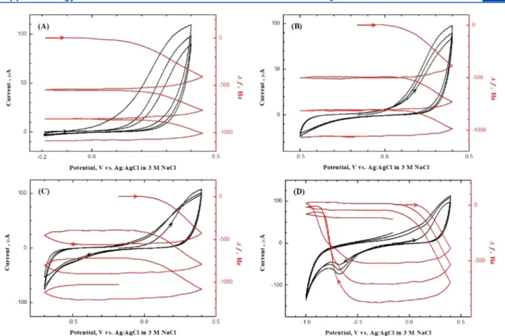
What happens when the potential window encompassed by the CV-EQCN data is systematically expanded? Figure 2 contains the results; the termination potential was expanded systematically from −0.2 V (Figure 2A) to −1.0 V (Figure 2D). The positive potential limit was maintained constant in all of the cases at +0.4 V. The data inFigure 2A reflectreaction 1, and no film dissolution was observed during the returning negative-going scans, as indicated by the fact that the EQCN frequency remained constant. When the potential window was extended to more negative potentials, cathodic stripping of the anodically deposited MoSxfilm (according to the reverse of reactions 1and2) was observed during the cathodic scan, as evidenced from the frequency increase from∼−0.5 V (Figure 2B) until the potential scan was reversed at −0.7 V (Figure 2C). The increase in frequency continued until the potential was scanned to∼0.0 V. As the potential was further scanned to
−1.0 V (Figure 2D), the decrease in frequency could be seen at potentials beyond∼−0.9 V. As mentioned earlier, this signaled the formation of MoS2viareactions 3and4. A subtle aspect of these data is that MoSxfilms were cathodically stripped in two distinct stages only in thefirst cycle (Figures 1and2D).
Figure 3shows an LSV scan with EQCN frequency changes for a MoSx-modified Au electrode in a 0.1 M KNO3 blank Figure 1. Cyclic voltammograms (black lines) along with EQCN
frequency changes (red lines) for a Au electrode in a 0.1 M KNO3 electrolyte containing 2 mM (NH4)2MoS4(pH = 6.5). The arrows indicate the potential scan direction. Scan rate: 50 mV/s.
ACS Applied Energy Materials www.acsaem.org Article
electrolyte (pH = 6.5). As shown in the figure, a cathodic current flow increased slowly without concomitant frequency change until the potential was scanned to about−0.6 V, when a composite twin cathodic wave at∼−0.75 V appeared with a mass decrease in two distinct stages. A slight mass gain at negative potentials of ∼−1.0 V also mimics the trends seen above. Thus, the essential features on thefirst return stripping scan in Figures 1and 2D were also captured here. The two- stage stripping sequence seen in thefirst cycle in thesefigures may be accommodated by the possibility that the MoSx film
contains different species.4,8 Alternatively, initial stripping can be assigned to the dissolution of surface layers, followed by the stripping of bulk layers.
No cathodic wave or frequency changes at∼−0.75 V were observed in a control LSV-EQCN scan after potential cycling of the MoSx-modified electrode between 0.0 and−0.7 V at 50 mV/s in a 0.1 M KNO3blank electrolyte (pH = 6.5) (Figure S1). Clearly, the first feature of the stripping sequence disappeared during the precycling treatment.
The sulfur in MoS3possesses a different oxidation state from sulfur in MoS2 contrasting with the oxidation state of molybdenum, which is +4 in both MoS2 and MoS3. MoS3 contains bridging S−S2−and S2−anions with a theoretical ratio of 1:1.7 Figure S2 contains X-ray photoelectron spectroscopy (XPS) data for a MoS3film electrodeposited in a 0.1 M KNO3 electrolyte containing 2 mM (NH4)2MoS4 at +0.4 V for 1 h.
The signal with binding energy at 229.3 eV (Figure S2A) in the high-resolution Mo 3d region is attributed to the Mo(IV) ions in MoS3.4,7 Another set of peaks at 232.5 and 235.6 eV is assigned to the Mo(VI) species in MoO3, formed adventi- tiously during the electrodeposition and/or sample transfer during the measurement. A peak at 226.6 eV due to S 2s appeared next to the Mo 3d region.36The peak at the binding energy of 162.9 eV in the S 2p region (Figure S2B) can be assigned to bridging S22−.4 Elemental analysis by energy- dispersive X-ray (EDX) revealed an atomic ratio of S/Mo in thesefilms to be∼3.8 (Figure S2C,D), a value consistent with that expected fromreaction 1. Thus, the XPS and EDX data, taken together, confirmed the successful oxidative deposition of MoS3with elemental sulfur on the FTO substrate.
Figure 2.Cyclic voltammograms (black line) along with EQCN frequency changes (red line) for a Au electrode in a 0.1 M KNO3electrolyte containing 2 mM (NH4)2MoS4(pH = 6.5) with increasingly negative potential limits, (A)−0.2 V, (B)−0.5 V, (C)−0.7, and (D)−1.0. Scan rate:
50 mV/s.
Figure 3. Linear sweep voltammogram (black line) with EQCN frequency changes (red line) for the MoSx-modified Au electrode in a 0.1 M KNO3 electrolyte (pH = 6.5). The MoSx film was electrodeposited at +0.4 V for 160 s in a 0.1 M KNO3 electrolyte containing 2 mM (NH4)2MoS4. Scan rate: 50 mV/s.
2.2. Activation of the Electrodeposited MoSxSurface.
This is key to our strategy to convert the MoSxlayers to CdS/
MoS2 heterostructures, as described in the next section. For now, we explore the nuances of the activation step. Activation, herein, refers to the irreversible reductive removal of S atoms (see above) from the MoSxsurface, leaving behind MoS2.4,5To this end, LSV-EQCN experiments were conducted on a MoSx- modified electrode (as inFigure 3) in 0.5 M H2SO4 (pH = 0.3).
When the pH of the supporting electrolyte was decreased from 6.5 to 3.5 using H2SO4 (Figure 4A), trends in voltammograms and frequency changes were maintained except for increased frequency changes after∼−1.1 V. Recall that this is assignable to the reduction of MoS42−to MoS2(see above). The observed EQCN frequency change in Figure 4A suggested that dissolution to MoS42−and reduction to MoS2 occurred together during the cathodic scan, as diagnosed from the incomplete stripping of the MoSxfilm at∼−1.1 V.
When pH was further lowered to 0.3, the cathodic current monotonically increased with potential while the frequency change was almost stable after∼−0.5 V, implying stability of the electrogenerated MoS2films in an acidic electrolyte (Figure 4B). Considering the slow deposition of MoS2films at negative potentials due to the competing HER and fast oxidative deposition of MoSx, as shown in Figure 1, conversion of anodically deposited MoSxinto MoS2could be an alternative strategy for the controlled electrosynthesis of MoS2.
The systematic shift in the onset of (the monotonic) cathodic currentflow to more positive potentials as the pH was lowered (from∼6.5 to 3.5,Figures S1and4A,B, and 0.3) was entirely consistent with the trend to be expected for the HER.
The successful transformation (activation) of MoSx into MoS2was further confirmed by XPS and EDX analysis (Figure S3). Again, signals with binding energy at 229.3 and 232.5 eV (Figure S3A) were attributed to Mo(IV) in MoS2and Mo(VI) in MoO3, respectively.4,7,8 The peak at 161.9 eV in the S 2p region (Figure S3B) was due to terminal S2−.4,9Again, the peak at the binding energy of 162.9 eV can be assigned to the bridging S22−.4 Another peak at 168−171 eV was assigned to sulfate adsorbed on the surface.16EDX analyses of the MoS2 films converted from MoSx afforded an elemental stoichio- metric atomic ratio of ∼1:2.3 (Figure S3C,D), as expected from the successful synthesis of MoS2 from anodically electrodeposited MoSxfilms. The results from XPS and EDX in Figures S2 and S3 confirmed that MoS3 was anodically
electrodeposited by oxidation of MoS42−and thus-synthesized MoS3 was successfully transformed into MoS2 by electro- reduction. Scanning electron microscopy (SEM) images of anodically deposited MoSx films and MoS2films (Figures S2 and S3) indicated thatfilms consisted of nanoparticles clearly segregated and uniformly distributed on the substrates.
2.3. Transformation of the Activated MoSxSurface to CdS/MoS2 and Characterization of Product. Shown in Figure 5is a linear sweep voltammogram accompanied by the
corresponding EQCN frequency change for a MoSx-modified electrode in 0.5 M H2SO4also containing 10 mM CdSO4. The MoSxfilms were pre-electrodeposited on the Au substrate by the same procedure as shown inFigure 3.
Contrasting with the increase (mass decrease) in the frequency in a 0.5 M H2SO4 blank electrolyte (Figure 4), thedecreasein frequency (mass increase) started at∼−0.5 and continued until∼−1.0 V, followed by a substantial decrease due to deposition of bulk cadmium beyond ∼−1.0 V. A cathodic wave at−0.5 V is due to the reduction of MoSxinto MoS2and sulfide, which resulted in CdS/MoS2by the reaction of Cd2+with sulfide ions or hydrogen sulfide
Figure 4.Linear sweep voltammogram (black line) along with EQCN frequency changes (red line) for a MoSx-modified electrode in (A) 0.1 M KNO3electrolyte (pH = 3.5) and (B) 0.5 M H2SO4(pH = 0.3). Scan rate: 20 mV/s.
Figure 5.Linear sweep voltammogram (black line) along with EQCN frequency changes (red line) for the MoSx-modified electrode in 0.5 M H2SO4 containing 10 mM CdSO4. Inset: A control linear sweep voltammogram (black line) along with EQCN frequency changes (red line) for a bare Au electrode in 0.5 M H2SO4 containing 10 mM CdSO4. Scan rate: 20 mV/s.
ACS Applied Energy Materials www.acsaem.org Article
H S2 + Cd2+→CdS+2H+ (5) The inset shows a control linear sweep voltammogram along with EQCN frequency changes for a bare Au electrode in 0.5 M H2SO4 containing 10 mM CdSO4, which proves that the deposition in Figure 5 that began at ∼−0.5 V is from the formation of CdS, not cadmium.
Laser Raman spectroscopy, XPS, EDX, and SEM were performed to probe the composition and morphology of the CdS/MoS2 heterostructures. To this end, a MoSx film was anodically electrodeposited on the FTO electrode at +0.4 V for 1 h from a 0.1 M KNO3 electrolyte containing 2 mM (NH4)2MoS4. Next, the MoSx-modified electrode was subjected to potentiostatic reduction at−0.6 V for 30 min in 0.5 M H2SO4containing 10 mM CdSO4. Figure 6A shows a Raman spectrum for the resultant sample. The peaks at 297.7 and 595.5 cm−1were characteristic 1 LO and 2 LO vibrational modes for CdS.18,22Additional peaks at 376 and 406 cm−1in the inset were indexed to the E2gand A1gvibrational modes of MoS2,18,22indicating successful conversion of MoSxto MoS2. MoS2is built from layers of Mo sandwiched between layers of S, and Raman spectroscopy has been used to determine the number of layers using frequency difference.37The observed frequency difference of ∼30 cm−1 implied that MoS2 was deposited as a bulkfilm rather than as a few monolayers.37The attenuation of the MoS2Raman signals (seeFigure 6A and the
inset) could be ameliorated by shrinking the reduction time to 500 s; now the relative intensity trend was reversed (seeFigure S4).
XPS was employed to further investigate the surface chemical composition and valence state of the various elements in the CdS/MoS2sample. Two peaks at 405.0 and 411.8 eV were assigned to Cd 3d5/2and 3d3/2, respectively, characteristic of Cd2+ in CdS (Figure 6B).18,19,21 The peaks at binding energies of 229.3 and 232.3 eV (Figure 6C) were again assigned to Mo(IV) in MoS2 and Mo(VI) in MoO3, respectively.4,7 Next to the Mo 3d doublets, a singlet with a binding energy of 226.9 eV is from S 2s, which is also a typical feature of MoS2.4,18Similarly, peaks at 162.9 and 161.6 eV in the S 2p spectrum (Figure 6D) corresponded to the oxidation state of S2− in MoS2. EDX analysis also confirmed that the ratio of Cd/Mo/S was ∼1:1:3, demonstrating formation of CdS/MoS2(Figure S5).
The morphology of the CdS/MoS2 samples was charac- terized by SEM and EDX elemental mapping measurements. A typical SEM image displayed inFigure 7A revealed spherical CdS/MoS2particles with a diameter ranging from 0.49 to 1.75 μm, uniformly deposited on the MoS2layers. The inset shows a magnified CdS/MoS2particle revealing that the morphology was very different from MoS2or MoS3(cf.,Figures 7A andS2, S3). A side view of the composite in Figure 7B shows that CdS/MoS2particles were formed on the MoS2 layer that, in Figure 6.(A) Laser Raman spectrum and high-resolution X-ray photoelectron spectra for CdS/MoS2in (B) Cd 3d, (C) Mo 3d, and (D) S 2p binding energy region. See the text for sample preparation details. The excitation wavelength for the Raman spectrum was 532.05 nm.
turn, was transformed from MoSx. Elemental mapping measurements of a single particle in Figure 7B clearly demonstrated that S, Mo, and Cd were homogeneously dispersed in the particle (Figure 7C). X-ray diffraction of the as-prepared CdS/MoS2 particles indicated them to be amorphous.
High-resolution transmission electron microscopy (HR- TEM) images of a CdS/MoS2 particle (Figure 8) showed
that the CdS particles did not merely sit on a MoS2 layer.
Instead, these data confirmed the SEM-based conclusions mentioned above that CdS/MoS2particles were formed on the (underlying) MoS2 layer. The lattice fringes from the (200) planes in CdS and the (002) planes in MoS2 were clearly visible (Figure 8b) and attested to heterojunction formation.
Films prepared on Au/quartz supports for EQCN measure- ments are not optimal for photoelectrochemical (PEC) characterization because they are too thin. Therefore, micro- meter-thick CdS/MoS2 films were electrosynthesized for this specific purpose (see Experimental Section below for details).
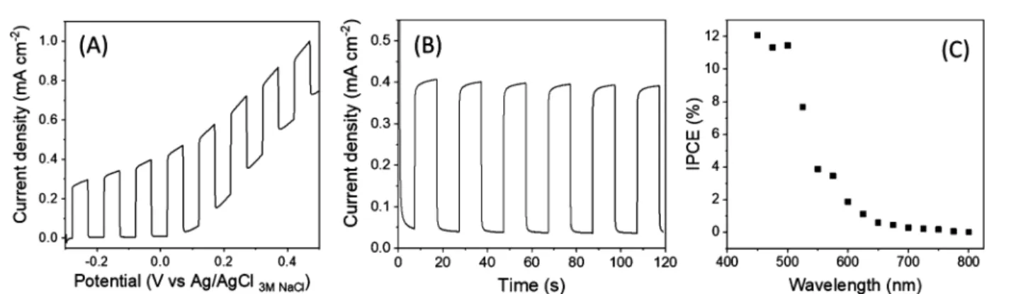
The PEC activity and internal-photon-to-electron-conversion efficiency (IPCE) of the CdS/MoS2 samples were evaluated using sulfite as a redox probe. Sodium sulfite is a facile hole scavenger for this purpose.Figure 9A shows the PEC activity of an electrodeposited and heat-treated CdS/MoS2film under chopped light illumination. Compared to the negligible photocurrent for the bare CdS and MoS2 samples (Figures S6 and S7), the photocurrent was significantly enhanced for the CdS/MoS2heterojunction electrode, reaching ca. 0.4 mA cm−2 at +0.1 V (vs Ag/AgCl). Figure 9B contains corresponding transient photocurrent data at afixed potential of +0.1 V in the same electrolyte. The good rectangularity of the photocurrent transients in Figure 9B and the relative absence of spikes diagnosed that electron−hole recombination was suppressed by heterojunction formation. This is consistent with the proposed vectorial carrier separation, as shown in Figure 10. Such an enhancement mechanism has been discussed before in the literature (cf., refs 18 and 19). The IPCE trace (action spectrum) of the CdS/MoS2 film is displayed in Figure 9C. The maximum IPCE was achieved below 500 nm, with a cutoff value at ∼580 nm. This value suggested that the majority of the photocurrent originated from the CdS part of the heterojunction electrode, and the role of MoS2 was simply to promote the vectorial separation of charge carriers generated in CdS (mostly by siphoning Figure 7.SEM images of CdS/MoS2: (A) top view and (B) side view. The inset in the A frame shows a typical CdS/MoS2particle. (C) Elemental mapping images of S, Mo, and Cd in the particle.
Figure 8.(A) HR-TEM image CdS/MoS2particles inFigure 7after thermal annealing at 400°C for 60 min in a nitrogen atmosphere and (B) magnified image of the selected frame from image (A).
ACS Applied Energy Materials www.acsaem.org Article
electrons before they recombined with the photogenerated holes in CdS, seeFigure 10).
Additional, conclusive evidence for heterojunction formation between CdS and MoS2 was accrued from surface photo- voltage spectroscopy (SPS) and Kelvin probe measurements.
SPS was applied to probe the contributions of CdS and MoS2 to the photovoltage in the heterojunction (Figure S8). Two maxima could be seen in the photovoltage spectrum around 550 and 800 nm corresponding to the band gaps of CdS (2.4 eV) and MoS2(1.3 eV).38,39The contact potential difference (CPD) values (Figure S8) (replicated three times) were: 325
±5, 590±4, and 542± 11 meV for CdS, MoS2, and CdS/
MoS2samples, respectively. The Fermi levels calculated using these CPD values were ca.−4.7,−5.0, and−4.9 eV in the case of CdS, MoS2, and CdS/MoS2 samples, respectively. This confirmed that there was Fermi level equilibration in the heterojunction. Based on the valence bond (VB) energy values (from ambient pressure ultraviolet (UV) appearance photo- electron spectroscopy (APS) measurements) and the optical band-gap information, a band diagram of the CdS/MoS2
heterojunction was constructed (Figure 10), which shared features with those reported in the literature was observed.38,39 Further optimizations of the CdS/MoS2 heterojunction, beyond the scope of this study, would be needed for these samples to be utilized in practical applications such as the HER 3. MATERIALS AND METHODS
Ammonium tetrathiomolybdate ((NH4)2MoS4), sodium sulfide (Na2S), cadmium sulfate hydrate (CdSO4·8/3H2O), potassium nitrate (KNO3), and sodium sulfite (Na2SO3) were bought from Sigma-Aldrich and used without further purification. The pH of each solution was adjusted with 1 M H2SO4 or 1 M NaOH, as needed.
Details of the electrochemical instrumentation including the potentiostat, electrodes, and EQCN are given elsewhere.31−34Briefly, all electrochemical experiments were performed at room temperature in a conventional three-electrode cell using an AT-cut, Au-coated quartz crystal (geometric area, 0.2 cm2) working electrode, a Pt counter electrode, and a Ag/AgCl/3 M NaCl reference electrode. All potentials mentioned above are quoted with respect to this reference electrode. The electrolytes were degassed with high-purity nitrogen prior to the electrochemical measurements, and a nitrogen blanket was used during measurement.
The photoelectrochemical (PEC) experiments were performed per details given elsewhere.33 Briefly, a sealed, custom-designed one- compartment, three-electrode glass cell was used. A MoSx film was anodically electrodeposited on the FTO electrode using consecutive depositions steps at +0.3 +0.4, and +0.5 V for 300 s, from a 0.1 M KNO3 electrolyte containing 2 mM (NH4)2MoS4. Next, the MoSx- modified electrodes were subjected to potentiostatic reduction at
−0.5,−0.6, and−0.7 V for 300 s in 0.5 M H2SO4containing 10 mM CdSO4solution, resulting in the CdS/MoS2sample. For comparative purposes, MoS2 and CdS films were also electrosynthesized. The MoS2film was deposited at +0.3 +0.4, and +0.5 V for 300 s from a 0.1 M KNO3 electrolyte containing 2 mM (NH4)2MoS4, and then activated at−0.5,−0.6, and−0.7 V for 300 s in 0.5 M H2SO4. A CdS film was also deposited at−0.5,−0.6, and−0.7 V for 300 s in 0.5 M H2SO4containing 10 mM CdSO4. The electrochemically deposited films were heat-treated at 400°C in a tube furnace for 30 min in Ar flow (150 cm3/min) prior to use.
The depositedfilms were irradiated with a 300 W xenon arc lamp contained in a Muller Elektronik-Optik LAX 1530 housing and connected to a Muller Elektronik-Optik SVX 1530 power source. The incident light intensity on the electrode surface, as measured with a Newport model 70260 radiant power meter/model 70268 probe, was
∼100 mW/cm2in all experiments described below. The exposed area of the indium tin oxide (ITO) surface was 0.2 cm2. In other measurements (in Szeged), modified FTO electrodes were used as the working electrode, with a Pt plate and Ag/AgCl/3 M NaCl being employed as counter and reference electrodes, respectively. The applied light source was a Newport LCS-100 type solar simulator operated at full output. The radiation source was placed 18 cm away Figure 9.Photoelectrochemical activity of CdS/MoS2films in a 0.1 M Na2SO3solution. (A) Photovoltammogram recorded at a scan rate of 5 mV/
s. (B) Transient photocurrent profile and (C) photoaction spectrum. The data in frames (B) and (C) were acquired at afixed potential of +0.1 V vs Ag/AgCl.
Figure 10. Band diagram, together with proposed charge carrier paths, constructed from the Kelvin probe data (Figure S9) and optical data from the literature (refs38,39).
from the illuminated working electrode surface (100 mW cm−2flux).
The cell contained an aqueous solution of 0.1 M Na2SO3, which was saturated with Ar. Photovoltammograms were recorded using 5 mV s−1potential sweep in parallel with periodically interrupted irradiation (0.1 Hz). IPCE measurements were carried out on a Newport Quantum Efficiency Measurement System (QEPVSI-B) in the same single-compartment, three-electrode electrochemical cell. The wave- length range was 800−400 nm (Δλ= 25 nm step size). The CdS/
MoS2-modified FTO electrode was held at +0.1 V constant potential during the measurements. The electrochemically active area of the film on the FTO surface was 1 cm2in these cases.
Film morphology and composition were obtained on a JEOL model JSM-7610F ultrahigh-resolution field-emission scanning electron microscope (FESEM) equipped with an energy-dispersive X-ray emission analysis (EDX) probe. High-resolution transmission electron microscopy (HR-TEM) used a JEOL model JEM-2100F instrument. For the TEM sample preparation, the particles were scraped offthe support electrode surface.34They were then dispersed by sonication in methanol followed by immobilization on a carbon grid for examination. Prior to the examination, the particles were thermally annealed as needed.
X-ray photoelectron spectra were obtained on a Ulvac-PHI Model PHI Quantera-II instrumentfitted with a monochromatic Al KαX-ray source. Laser Raman spectra were obtained on a Nanophoton model RAMANtouch spectrometer equipped with a 532.05 nm laser and a grating with 2400 lines mm−1. Contact potential differences (CPDs), surface photovoltage spectroscopy (SPS), and ambient pressure ultraviolet (UV) appearance photoelectron spectroscopy (APS) were measured on a KP Technology APS04 Kelvin probe instrument equipped with a 2 mm diameter gold alloy-coated tip. The Fermi level (EF) of the tip was determined relative to a silver reference target (EF, Au tip = −4.40 eV). Instrumentation details for other photo- electrochemical measurements are given elsewhere.40
4. CONCLUSIONS
This work has demonstrated a general approach to electro- synthesizing heterojunctions based on two metal chalcoge- nides. The key is to be able to activate the underlying
“precursor” chalcogenide surface by suitable electrochemical pretreatment. Thereby, the interfacial activity of a reactive chalcogenide species serves to generate the overlayer as needed after the electrolyte composition is appropriately modified.
This approach was illustrated here for the specific instance of CdS/MoS2 using an anodically electrodeposited MoSx
“template” layer. This layer was electroreductively activated to generate MoS2 and S2− species. Subsequent interfacial precipitation of added Cd2+ with the interfacial S2− species resulted in CdS/MoS2 nanoparticle formation on the MoS2 bottom layer. Heterojunction formation was confirmed by HR- TEM as well as via Kelvin probe measurements of the CPDs.
The resultant CdS/MoS2 heterojunctions showed enhanced PEC activity relative to its components. However, further optimizations would be needed to translate thesefindings to practical HER (or other electrocatalysis/photocatalysis) applications.
■
ASSOCIATED CONTENT*sı Supporting Information
The Supporting Information is available free of charge at https://pubs.acs.org/doi/10.1021/acsaem.1c00814.
LSV-EQCN data, high-resolution XPS data, laser Raman spectral data, EDX profiles, photovoltammetry, and Kelvin probe measurement results (PDF)
■
AUTHOR INFORMATION Corresponding AuthorsNoseung Myung−Department of Applied Chemistry, Konkuk University Glocal Campus, Chungju, Chungbuk 27478, Korea; Email:myung@kku.ac.kr
Krishnan Rajeshwar−Department of Chemistry&
Biochemistry, The University of Texas at Arlington, Arlington, Texas 76109, United States; orcid.org/0000- 0003-4917-7790; Email:rajeshwar@uta.edu
Authors
Kongshik Rho−Department of Applied Chemistry, Konkuk University Glocal Campus, Chungju, Chungbuk 27478, Korea
Eun Bee Sohn− Department of Applied Chemistry, Konkuk University Glocal Campus, Chungju, Chungbuk 27478, Korea
Su Jin Lee− Department of Applied Chemistry, Konkuk University Glocal Campus, Chungju, Chungbuk 27478, Korea
Peter S. Toth−University of Szeged, Szeged H-6720, Hungary
Abbas Vali−Department of Chemistry&Biochemistry, The University of Texas at Arlington, Arlington, Texas 76109, United States
Csaba Janáky− University of Szeged, Szeged H-6720, Hungary; orcid.org/0000-0001-5965-5173 Complete contact information is available at:
https://pubs.acs.org/10.1021/acsaem.1c00814
Notes
The authors declare no competingfinancial interest.
■
ACKNOWLEDGMENTSThis research was supported by the Basic Science Research Program through the National Research Foundation of Korea ( N R F ) , t h e M i n i s t r y o f E d u c a t i o n ( N R F - 2016R1D1A1B02010133). P.S.T. was supported by the János Bolyai Research Scholarship of the Hungarian Academy of Sciences and supported by the ÚNKP-20-5 New National Excellence Program of the Ministry for Innovation and Technology (National Research, Development and Innovation Fund). K.R. thanks Profs. Efstathios Meletis and Seong Jin Koh (Materials Science & Engineering, The University of Texas at Arlington) for discussion. Finally, two anonymous reviewers are thanked for constructive criticisms of an earlier manuscript version.
■
(1) Rajeshwar, K.; Macaluso, R. Chalcogenides: Solid-StateREFERENCES Chemistry. In Encyclopedia of Inorganic and Bioinorganic Chemistry;John Wiley & Sons: New York, 2020.
(2) Morales-Guio, C. G.; Hu, X. Amorphous Molybdenum Sulfides as Hydrogen Evolution Catalysts. Acc. Chem. Res.2014,47, 2671−
2681.
(3) For example: Voiry, D.; Salehi, M.; Silva, R.; Fujita, T.; Chen, M.; Asfa, T.; Shenoy, V.; Eda, G.; Chhowalla, M. Conducting MoS2 Nanosheets as Catalysts for Hydrogen Evolution Reaction.Nano Lett.
2013, 6222−6227.
(4) Vrubel, H.; Hu, X. Growth and Activation of an Amorphous Molybdenum Sulfide Hydrogen Evolving Catalyst.ACS Catal.2013, 3, 2002−2011.
(5) Mabayoje, O.; Liu, Y.; Wang, M.; Shoola, A.; Ebrahim, A. M.;
Frenkel, A. I.; Mullins, C. B. Electrodeposition of MoSx Hydrogen
ACS Applied Energy Materials www.acsaem.org Article
Evolution Catalysts from Sulfur-Rich Precursors. ACS Appl. Mater.
Interfaces2019,11, 32879−32886.
(6) Merki, D.; Fierro, S.; Vrubel, H.; Hu, X. Amorphous Molybdenum Sulfide Films as Catalysts for Electrochemical Hydro- gen Production in Water.Chem. Sci.2011,2, 1262−1267.
(7) Zhang, W.; Zhou, T.; Zheng, J.; Hong, J.; Pan, Y.; Xu, R. Water- Soluble MoS3 Nanoparticles for Photocatalytic H2 Evolution.
ChemSusChem.2015,8, 1464−1471.
(8) Wu, Q.; Abraham, A.; Wang, L.; Tong, X.; Takeuchi, E. S.;
Takeuchi, K. J.; Marschilok, A. C. Electrodeposition of MoSx: Tunable Fabrication of Sulfur Equivalent Electrodes for High Capacity or High Power.J. Electrochem. Soc.2020,167, No. 050513.
(9) Wang, T.; Du, K.; Liu, W.; Zhang, J.; Li, M. Electrochemical Sensors Based on Molybdenum Disulfide Nanomaterials. Electro- analysis2015,27, 2091−2097.
(10) Falola, B. D.; Wiltowski, T.; Suni, I. I. Electrodeposition of MoS2 for Charge Storage in Electrochemical Supercapacitors. J.
Electrochem. Soc.2016,163, D568−D574.
(11) Rajeshwar, K. Electrosynthesized Thin Films of Group II-VI Compound Semiconductors, Alloys and Superstructures.Adv. Mater.
1992,4, 23−29.
(12) Ponomarev, E. A.; Neumann-Spallart, M.; Hodes, G.; Levy- Clement, C. Electrochemical Deposition of MoS2 Thin Films by Reduction of Tetrathiomolybdate.Thin Solid Films1996,280, 86−89.
(13) Ponomarev, E. A.; A-Yaron, A.; Tenne, R.; L-Clement, C.
Electrochemical Deposition of Quantized Particle MoS2Thin Films.J.
Electrochem. Soc.1997,144, L277−L279.
(14) Thomas, S.; Smith, D. E.; Greenacre, V. K.; Noori, Y. J.;
Hector, A. L.; de Groot, C. H.; Reid, G.; Bartlett, P. N.
Electrodeposition of MoS2 from Dichloromethane. J. Electrochem.
Soc.2020,167, No. 106511.
(15) Redman, D. W.; Rose, M. J.; Stevenson, K. J. Electrodeposition of Amorphous Molybdenum Chalcogenides from Ionic Liquids and Their Activity for the Hydrogen Evolution Reaction.Langmuir2017, 33, 9354−9360.
(16) Li, Q.; Walter, E. C.; van der Veer, W. E.; Murray, B. J.;
Newberg, J. T.; Bohannan, E. W.; Switzer, J. A.; Hemminger, J. C.;
Penner, R. M. Molybdenum Disulfide Nanowires and Nanoribbons by Electrochemical/Chemical Synthesis. J. Phys. Chem. B 2005, 109, 3169−3182.
(17) Zong, X.; Yan, H.; Wu, G.; Ma, G.; Wen, F.; Wang, L.; Li, C.
Enhancement of Photocatalytic H2 Evolution on CdS by Loading MoS2as Cocatalyst under Visible Light Irradiation.J. Am. Chem. Soc.
2008,130, 7176−7177.
(18) Lin, L.; Huang, S.; Zhu, Y.; Du, B.; Zhang, Z.; Chen, C.; Wang, X.; Zhang, N. Construction of CdS/MoS2 Heterojunction from Core−Shell MoS2@Cd-MOF for Efficient Photocatalytic Hydrogen Evolution.Dalton Trans.2019,48, 2715−2721.
(19) Liu, Y.; Yu, Y.-X.; Zhang, W.-D. MoS2/CdS Heterojunction with High Photoelectrochemical Activity for H2 Evolution under Visible Light: The Role of MoS2.J. Phys. Chem. C2013,117, 12949− 12957.
(20) Li, L.-L.; Yin, X.-L.; Pang, D.-H.; Du, X.-X.; Xue, H.; Zhou, H.- W.; Yao, Q.-X.; Wang, H.-W.; Qian, J.-C.; Yang, J.; Li, D.-C.; Dou, J.- M. One-pot Synthesis of MoS2/CdS Nanosphere Heterostructures for Efficient H2Evolution under Visible Light Irradiation.Int. J. Hydrogen Energy2019,44, 31930−31939.
(21) Zheng, Z.; Qiao, Y.; Cai, Y.; He, Y.; Tang, Y.; Li, L. MoS2 Decorated CdS Hybrid Heterojunction for Enhanced Photoelec- trocatalytic Performance under Visible Light Irradiation. J. Colloid Interface Sci.2019,533, 561−568.
(22) Zheng, W.; Feng, W.; Zhang, X.; Chen, X.; Liu, G.; Qiu, Y.;
Hasan, T.; Tan, P.; Hu, P. A. Anisotropic Growth of Nonlayered CdS on MoS2 Monolayer for Functional Vertical Heterostructures. Adv.
Funct. Mater.2016,26, 2648−2654.
(23) Ji, J.; Sun, B.; Shan, F.; Li, Q.; Huang, F.; Song, Y.; Wang, F.
Optimization of CdS@MoS2 Core-Shell Nanorod Arrays for Enhanced Photoresponse for Photo-Assistant Electrochemical Water
Splitting under Solar Light Illumination.RSC Adv.2016,6, 100115−
100121.
(24) Zhu, X.; Wang, P.; Zhang, Q.; Wang, Z.; Liu, Y.; Qin, X.;
Zhang, X.; Dai, Y.; Huang, B. CdS-MoS2 Heterostructures on Mo Substrates via In Situ Sulfurization for Efficient Photoelectrochemical Hydrogen Generation.RSC Adv.2017,7, 44626−44631.
(25) Yin, X.-L.; Li, L.-L.; Jiang, W.-J.; Zhang, Y.; Zhang, X.; Wan, L.- J.; Hu, J.-S. MoS2/CdS Nanosheets-on-Nanorod Heterostructure for Highly Efficient Photocatalytic H2 Generation under Visible Light Irradiation.ACS Appl. Mater. Interfaces2016,8, 15258−15266.
(26) Li, Q.; Shan, F.; Sun, B.; Song, Y.; Wang, F.; Ji, J. Photo- Assisted Electrocatalysis of CdS-MoS2 Hybrid for Hydrogen Evolution Reaction: Morphology-Dependent Photoelectroactivity of p-n Junction Photocathode under Bias Potential. Int. J. Hydrogen Energy2017,42, 5549−5559.
(27) Zhang, J.; Zhu, Z.; Feng, X. Construction of Two-Dimensional MoS2/CdS p-n Nanohybrids for Highly Efficient Photocatalytic Hydrogen Evolution Reaction. Chem. - Eur. J. 2014, 20, 10632−
10635.
(28) Zong, X.; Wu, G.; Yan, H.; Ma, G.; Shi, J.; Wen, F.; Wang, L.;
Li, C. Photocatalytic H2 Evolution on MoS2/CdS Catalysts under Visible Light Irradiation.J. Phys. Chem. C2010,114, 1963−1968.
(29) Ji, J.; Guo, L.; Li, Q.; Wang, F.; Li, Z.; Liu, J.; Jia, Y. A Bifunctional Catalyst for Hydrogen Evolution Reaction: The Interactive Influences between CdS and MoS2on Photoelectrochem- ical Activity.Int. J. Hydrogen Energy2015,40, 3813−3821.
(30) Xu, J.; Cao, X. Characterization and Mechanism of MoS2/CdS Composite Photocatalyst Used for Hydrogen Production from Water Splitting under Visible Light.Chem. Eng. J.2015,260, 642−648.
(31) Jee, H.-W.; Paeng, K.-J.; Myung, N.; Rajeshwar, K. Electro- deposition of Cobalt Selenide Thin Films: An Electrochemical Quartz Crystal Microgravimetry Study.J. Electrochem. Soc.2017,164, D861−
D866.
(32) Jee, H.-W.; Paeng, K.-J.; Son, Y.; Jang, Y.; Rho, K.; Myung, N.
Electrosynthesis of Cobalt Telluride Thin Films by Voltammetry Combined with Electrochemical Quartz Crystal Microgravimetry.J.
Electrochem. Soc.2019,166, H3035−H3039.
(33) Myung, N.; Choi, S.; Lee, W.; Jeong, S.; Rajeshwar, K.
Synthesis of Au/ZnO Composite Nanorod Arrays via Electro- deposition Followed by Galvanic Replacement. ECS Electrochem.
Lett.2013,2, D33−D36.
(34) Jee, H.-W.; Paeng, K.-J.; Myung, N.; Rajeshwar, K. Electro- chemical Deposition of a Metal-Organic Framework and Subsequent Conversion to Cobalt Selenide.ACS Appl. Electron. Mater. 2020,2, 1358−1364.
(35) Myung, N.; Park, H.-Y.; Jee, H.-W.; Sohn, E. B.; Lee, S. J.;
Paeng, K.-J.; Rhee, I.; Vali, A.; Rajeshwar, K. Electrosynthesis of MoTe2 Thin Films: A Combined Voltammetry-Electrochemical Quartz Crystal Crystal Microgravimetry Study of Mechanistic Aspects.J. Electrochem. Soc.2020,167, No. 116510.
(36) Shang, M.; Qi, H.; Du, C.; Huang, H.; Wu, S.; Zhang, J.; Song, W. One-Step Electrodeposition of High-Quality Amorphous Molybdenum Sulfide/RGO Photoanode for Visible-Light Sensitive Photoelectrochemical Biosensing.Sens. Actuators, B2018,266, 71−
79.
(37) Lee, C.; Yan, H.; Brus, L. E.; Heinz, T. F.; Hone, J.; Ryu, S.
Anomalous Lattice Vibrations of Single and Few-Layer MoS2.ACS Nano2010,4, 2695−2700.
(38) Zheng, Z.; Qiao, Y.; Cai, Y.; He, Y.; Tang, Y.; Li, L. MoS2 Decorated CdS Hybrid Heterojunction for Enhanced Photoelec- trocatalytic Performance under Visible Light Irradiation. J. Colloid Interface Sci.2019,533, 561−568.
(39) Li, Y.; Xu, C.-Y.; Zhang, B.-Y.; Zhen, L. Work Function Modulation of Bilayer MoS2 Nanoflake by Backgate Electric Field Effect.Appl. Phys. Lett.2013,103, No. 033122.
(40) Vali, A.; Sarker, H. P.; Jee, H.-W.; Kormányos, A.; Firouzan, F.;
Myung, N.; Paeng, K.-J.; Huda, M. N.; Janáky, C.; Rajeshwar, K.
Electrodeposition of Silver Vanadate Films: A Tale of Two Polymorphs.ChemPhysChem.2019,20, 2635−2646.