Development of Complex Curricula for Molecular Bionics and Infobionics Programs within a consortial* framework**
Consortium leader
PETER PAZMANY CATHOLIC UNIVERSITY
Consortium members
SEMMELWEIS UNIVERSITY, DIALOG CAMPUS PUBLISHER
The Project has been realised with the support of the European Union and has been co-financed by the European Social Fund ***
**Molekuláris bionika és Infobionika Szakok tananyagának komplex fejlesztése konzorciumi keretben
***A projekt az Európai Unió támogatásával, az Európai Szociális Alap társfinanszírozásával valósul meg.
VLSI Design Methodologies
3D Integration
(VLSI tervezési módszerek)
(3D Integrációjú Áramkörök)
PÉTER FÖLDESY
The topics are covered in this chapter:
• Why to integrate circuits in 3D
• What are the existing solution
• Stacking of packages or chips in 3D
• Silicon growth, real 3D monolithic technology
• Waferlevel bonding
• 3D interconnect solutions
• Pros. and contra against 3D integration
• Thermal issues
• Test and yield problems
www.itk.ppke.hu
Section I
Why and how to integrate circuits in 3D
www.itk.ppke.hu
Why to integrate circuits in 3D
• The motivation to go 3D is basically threefold:
• Reach higher integration, smaller size
• Integrate non compatible technologies like different semiconductor technologies, nanotech and biotech systems
• 3D integration would allow multicore processors and other high
connectivity architectures to adopt interconnection topologies
Why to integrate circuits in 3D in details:
• include multifunctionality,
• increased performance,
• reduced power,
• small form factor,
• reduced packaging,
• Increased yield and reliability,
• flexible heterogeneous integration
www.itk.ppke.hu
Some idealistic advantages:
• The average wire length drops by a factor of Nlayers1/2.
• In a current three layer technology, the average wire length decreased by a factor of at most 31/2 or 42%.
• Power would drop by a factor of Nlayers1/2
• Wire (RC) delay would drop by a factor of Nlayers
• Combined with the limited number of interconnections and the self-heating caused performance drop, the result is
mostly reduction in energy and not speed!
The main approaches to achieve several goals:
• Stacking of packages or chips in 3D
• The individual planar layers are fabricated independently in a classic way. Later on the layers are combined.
• Silicon growth, real 3D monolithic technology
• The layers are built on each other step-by-step
• Waferlevel bonding and other back-end-of-the-line (BEOL) compatible technologies
• Wafer bonding is a process of joining two or more wafers prior to dicing and packaging.
• Interconnection could be wire bonding, micro bumbs,
www.itk.ppke.hu
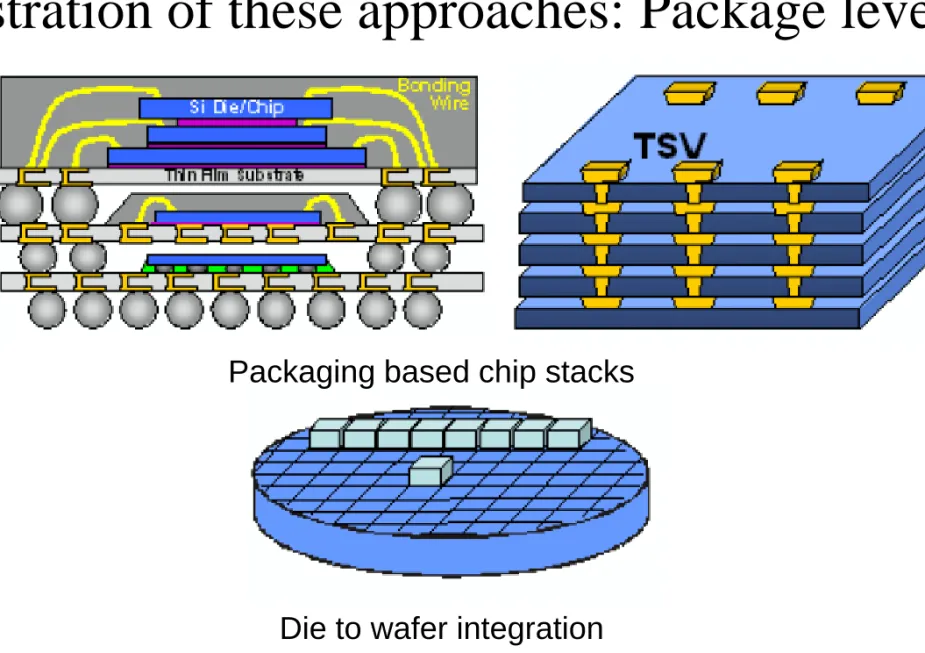
Illustration of these approaches: Package level
Packaging based chip stacks
Die to wafer integration
Illustration of these approaches: Silicon growth
Transistors formed inside the on-chip interconnect layer on a piece of
recrystallized silicon film
Transistors formed on single-crystal silicon films layer by layer
www.itk.ppke.hu
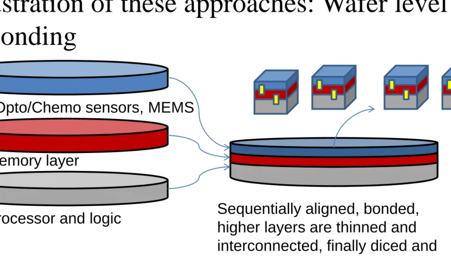
Illustration of these approaches: Wafer level bonding
Sequentially aligned, bonded, higher layers are thinned and interconnected, finally diced and packaged
Processor and logic Memory layer
I/Os, Opto/Chemo sensors, MEMS
Comparison of different technologies
Method Heterogeneous Testing (high yield)
Interlayer via density
Fabrication difficulty (price) Die stacking
(MCM)
Yes No Low (~100 um
pitch)
Low
Wafer bonding Yes No High (~5 um
pitch)
Medium
Silicon growth No No High Medium-High
Die to wafer Yes Yes High High
Section II
Detailed description of the different solutions
www.itk.ppke.hu
Die stacking (Multiple Chip Module – MCM)
• The simplest option for 3D integration is stacking of successively smaller dies.
• Die alignment requirements are not very precise
• Connection: wire bonding or flip-chip bonding
• While simple to produce, the benefits of die
stacking are limited. Connections are limited in number.
• Flip chips and multichip modules are now
www.itk.ppke.hu
Multiple Chip Module (MCM).
The idea is to decrease the average spacing between ICs in an electronic system compared to PCBs. The fundamental aspect of MCM technology is chip interconnection, which includes connecting I/O conductors on a chip to an substrate.
Multiple Chip Module (MCM).
POWER5 MCM with four processors and four 36 MB external L3 cache dies on a
ceramic multi-chip module.
Categories based on substrate:
• MCM-L - laminated MCM.
The substrate is a multi-layer laminated PCB.
• MCM-D - deposited MCM.
The modules are deposited on the base substrate using thin film technology.
• MCM-C - ceramic substrate.
www.itk.ppke.hu
Other stacked die solutions
• Mobile Internet devices (MIDs) are an obvious
target segment to benefit from the space, power and cost savings
• Cell phones are the primary consumers, Netbooks, Global Positioning System(GPS) systems and digital cameras are next in popularity.
• The stacked combinations:
• Logic + Memory, Logic + CMOS image sensors, stacked DRAM modules, Logic + MEMS and other sensors
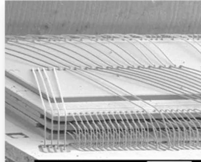
Illustration of the stacked dies
The dies are bonded out and to each other. The stack is placed in a BGA package.
Stacked dies with high density wire bonded interconnections
www.itk.ppke.hu
Wafer bonding
• Wafer bonding is a process of joining two or more wafers prior to dicing and packaging.
• Bonding creates interlayer (or intertier) vias while isolating the transistors from adjoining layers.
• Usually SOI layers are used, as the SOI process
scales better to many layers since each layer is very
thin, which aids in dissipating heat from the lower
layers.
Different approaches to Wafer bonding
• The challenge of developing a reliable, repeatable, low-cost bonding technology.
• Three different methods for wafer-level bonding today:
• 1) Metal-to-metal thermocompression bonding;
• 2) Conductive and non-conductive polymer adhesives
• 3) Direct oxide bonding (also known as “fusion,”
“covalent,” or “molecular” bonding).
• Each of these processes has both advantages and
www.itk.ppke.hu
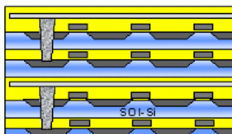
Wafer bonding styles
SOI face-to-back bonding with thin layers. Dashed line indicates bonded Interface.
Face-to-face bonding
Face-to-back bonding with thick layers and deep vias.
Silicon growth: Recrystallized layer forming
• Growing substrate layers above complete, metalized wafers. Typically special, power
transistors are created for better heat and power distribution.
• These techniques include Beam Recrystallization, Epitaxial Growth, and Solid Phase Crystallization.
• One drawback of these techniques is that layers
must be homogeneous since layers are created in
immediate succession on the same equipment.
Section III
3D interconnection solutions
www.itk.ppke.hu
3D Interconnection methods
• Wire bonding, classic technique in 2D as well
• Individual die are stacked and wire-bonded in this technique.
• Thermosonic ball and stitch bonding uses force, heat and ultrasonic energy to form both the ball and stitch bonds.
www.itk.ppke.hu
• Electrical proximity connection based on inductive or capacitive couplings:
• As reliable as wireline, much cheaper, scales very well.
• Inductive coupling. Less sensitive to distance, can transmit effectively power. Gain from multiple metal layers. It can reach a clock rate of 1-5 GHz and data rate of 1-5 Gb/s per channel crossing about 10 um spacing and 30-50 um pitch.
• Capacitive coupling needs less distant pads (few um), used in face-to-face interconnections.
• Through silicon vias, TSV
• There are two types of through via interconnect technologies.
• Through via bulk and through via Silicon on Insulator (SOI).
• Have the greatest interconnect density with disadvantage of the greatest cost.
• The first and second wafers are placed face to face and as the tier grows higher layers are placed face to back.
• Connection is provided by filling tungsten in DRIE etched wafers.
Comparison of interconnections
www.itk.ppke.hu
Technology Version Assembly Layer limit Vertical pitch
Wire bonded Die ~5 35-100 um
Mico-bump 3D package Die Heat 25-50 um
Micro-bump Face-to-face Die/wafer 2 10-100 um
Contactless Capacitive Die 2 50-200 um
Contactless Inductive Die Heat 30-100 um
TSV Bulk Wafer Heat, yield 50 um
TSV SOI Wafer Heat, yield 5 um
Section IV
Pros. and contra of 3D integration
www.itk.ppke.hu
Drawbacks of 3D integration
• Thermal issues
• Limited testability
• Yield
• Connection is much larger than active devices
• CAD tool support limited
• Mechanical problems
• Cost
Thermal issues
• Silicon has high thermal resistance
• Aside from costs and technological hurdles, the main challenge facing 3D integration is heat
dissipation.
• IC cooling has traditionally been handled by a heatsink attached to the top of the chip package.
• The 3D integration decreases the chip footprint,
increases self-heating and the power density at the
www.itk.ppke.hu
Thermal issues
• In a two layer 3D technology, the package thermal resistance must be roughly halved in order to
maintain the same temperature. That is not easy considering a 1 cm by 200 um die.
• The most promising technology is microchannels, which are etched into the substrate. It forms
channels through which cooling liquid could be pumped. Up to 100-200 W/cm
2operational!
• Dummy thermal vias are also used frequently.
Thermal issues: microchannels for cooling
Concept of IC with through-silicon vias (TSVs) and inter-layer cooling channels that is enclosed in a sealed case
Source: ETH Zurich in Switzerland
www.itk.ppke.hu
Thermal issues
• The increased heat density leads to degraded performance.
• Doubling the heat density without any improvement in
cooling capacity will lead to more than a 30% degradation in performance.
• Compare with the 42% speed advance in a hypothetical three layer technology that we calculated!
• Increased need for static and transient temperature
measurement during operation and thermal characterization.
• A possible way is to integrate temperature sensors in which field the Budapest University of Technology & Economics (BME) – EET developed outstanding solutions.
Thermal issues
• The thermal issues are less important in certain lower power devices like DRAMs.
• So, integrating DRAMs directly above CPUs may be a very attractive option since the DRAMs will not add much
power.
• Such solution is provided by Tezzaron Inc. with fixed layer structure and given memory layer.
• Note that the increased interconnect density gives not only thermal conductivity, but energy savings due to the
decreased interconnect capacitance
www.itk.ppke.hu
Testing and yield
• The electrical testing is limited in many solutions (except for later integration of known good dies).
• The electrical testing unfortunately strictly linked to mechanical and electrical analysis. Which is a crucial drawback of the 3D CAD tool development.
• The mechanical impact of the trench and the metal filling on the behavior of the CMOS components and the reliability is also unknown in depth.
Remember, the silicon is piezoresistive!
Connection is much larger than active devices
• The interconnection pitch is larger than the device size (due to TSV aspect ratio cannot be higher than 20-50, the wafer thickness cannot be less than 5-10 um. The current TSV pitch is roughly 2-5 um,
while device size is 20-30 nm).
• Dense interconnection causes congestion.
• No sense to split small modules, like logic gates.
www.itk.ppke.hu
Conclusions
• The 3D integration is propagated in many fields, like high density fast imagers, or mobile phone highly integrated system-in-a-packages (SiP).
• The main drawbacks are the yield, self-heating, testing
problems that has several exotic solutions (like microfluidic cooling channels inside the stacks).
• True 3D integration might be a reduction in power and size, rather than an increase in speed.
• The CAD tools and standards are not mature enough for real 3D integrated ICs.
Recommended literature
Handbook of 3D Integration: Technology and Applications of 3D Integrated Circuits (2 Vol. Set) Philip Garrou (Editor), Christopher Bower (Editor), Peter Ramm (Editor)
Publisher: Wiley-VCH (October 21, 2008)
www.itk.ppke.hu