Diamond & Related Materials 119 (2021) 108573
Available online 20 August 2021
0925-9635/© 2021 The Authors. Published by Elsevier B.V. This is an open access article under the CC BY-NC-ND license
(http://creativecommons.org/licenses/by-nc-nd/4.0/).
Diaphite-structured nanodiamonds with six- and twelve-fold symmetries
P ´ eter N ´ emeth
a,b,*, Kit McColl
c, Laurence A.J. Garvie
d, Christoph G. Salzmann
e, Chris J. Pickard
f,g, Furio Cor ` a
e, Rachael L. Smith
e, Mohamed Mezouar
h,
Christopher A. Howard
i, Paul F. McMillan
e,**aInstitute for Geological and Geochemical Research, Research Centre for Astronomy and Earth Sciences, E¨otv¨os Lor´and Research Network, Buda¨orsi út 45, 1112 Budapest, Hungary
bResearch Institute of Biomolecular and Chemical Engineering, University of Pannonia, Egyetem út 10, Veszpr´em 8200, Hungary
cDepartment of Chemistry, University of Bath, Bath BA2 7AX, UK
dCenter for Meteorite Studies, Arizona State University, Tempe, AZ 85287-6004, USA
eDepartment of Chemistry, University College London, 20 Gordon Street, London WC1H 0AJ, UK
fDepartment of Materials Science & Metallurgy, University of Cambridge, 27 Charles Babbage Road, Cambridge CB3 0FS, UK
gAdvanced Institute for Materials Research, Tohoku University, Aoba, Sendai 980-8577, Japan
hESRF-The European Synchrotron, 71 Avenue des Martyrs, Grenoble 38000, France
iDepartment of Physics & Astronomy, University College London, London, UK
A R T I C L E I N F O Keywords:
Nanodiamonds Diaphite
Ultra-high-resolution TEM Density functional calculations Six - and twelve-fold symmetries sp2- and sp3- bonded nanomaterials
A B S T R A C T
Nanodiamonds (ND) with 1-5 nm dimensions found in meteorites or produced by chemical vapour deposition (CVD) and detonation synthesis are typically described in terms of an sp3-bonded carbon network. However, ultra-high-resolution transmission electron microscopy (uHRTEM) combined with density functional theory (DFT) modelling leads to a different structural interpretation. uHRTEM imaging and nanodiffraction studies of many NDs show six-fold symmetry features whose identity has long been controversial. We also observe diffraction patterns with twelve equally-spaced and symmetrically but unequally arranged reflections, indicating structures with crystallographically-forbidden ideal and distorted twelve-fold symmetry. Structural models based on our DFT calculations lead to an interpretation of these unusual features found throughout the meteoritic and CVD samples in terms of sp3 domains arranged around and coherently bonded to graphitic domains embedded within the diamond matrix. The bonding at the sp2-sp3 interface can explain the unusual features observed in electron energy-loss spectra (EELS) below the onset of the main diamond C1s core-loss edge leading to pre- dictions of low-dimensional conductivity behaviour. The presence of sp2- as well as sp3-bonded regions allows us to interpret previously unexplained features of the Raman spectra and EELS data of ND materials.
1. Introduction
Nanodiamonds (ND) are 1-5 nm sized grains of carbon that are abundant in primitive meteorites. Understanding their origin and sig- nificance represent topics of intense interest leading to continued debate among planetary scientists [1–3]. Related carbon nanoparticles with ultrahard properties are formed by detonation synthesis from organic precursors [4], by laser ablation [5] and ball-milling processes [6]. Such materials have unique mechanical properties that are widely used in commercial abrasives and lubricants [7]. The high hardness and wear
resistance of diamond combined with the surface frictional properties of NDs leads to their incorporation in polymer and metallic nanocomposite blends [7]. Because of their adaptable surface chemistry and low toxicity, they are also being developed for biomedical applications [7–10]. Introducing nitrogen point defects produces paramagnetic N–V defects for field-emission [11], sensing [12], and quantum computing [13] applications, while fluorescent NDs for optoelectronics applications are now being prepared in nuclear reactors [14]. Chemical vapour deposition (CVD) techniques produce diamond thin films that are composed of <10-nm-sized ND domains, that exhibit unique
* Correspondence to: P. N´emeth, Institute for Geological and Geochemical Research, Research Centre for Astronomy and Earth Sciences, E¨otv¨os Lor´and Research Network, Buda¨orsi út 45, 1112 Budapest, Hungary.
** Corresponding author.
E-mail addresses: nemeth.peter@csfk.org (P. N´emeth), p.f.mcmillan@ucl.ac.uk (P.F. McMillan).
Contents lists available at ScienceDirect
Diamond & Related Materials
journal homepage: www.elsevier.com/locate/diamond
https://doi.org/10.1016/j.diamond.2021.108573
Received 8 July 2021; Received in revised form 11 August 2021; Accepted 16 August 2021
semiconducting and surface chemical properties, and high mechanical and chemical resistance, which make them ideal for a wide range of applications [15–16].
Studies of these ND materials by transmission electron microscopy (TEM), X-ray diffraction (XRD), and spectroscopic techniques, combined with computational predictions have led to the generally accepted view that their structures consist of an sp3-bonded diamond network. That interpretation is supported by the extreme hardness and mechanical resistance observed both for individual ND grains and thin films formed by CVD [16]. Both cubic (c) and hexagonal (h) stacking arrangements of the tetrahedrally bonded layers are determined to occur within ND grains [1,17], while other dense sp3-bonded structures have also been proposed [18–19]. Imaging, diffraction, and spectroscopic data also support the existence of C-H species, as well as other functional groups such as -COOH, decorating and passivating the surface of ND grains, and that both the ND grains as well as crystalline nanodomains within CVD samples might be covered by poorly crystalline graphite or amorphous carbon [7,20–22]. Although the ensemble of these observations and interpretations appear to constitute a complete and consistent picture of the internal structure of NDs, they do not explain key features of high- resolution TEM (HRTEM) imaging and nanodiffraction results, or pre- edge features observed in electron-energy loss spectroscopy (EELS) data [23–24], or the Raman spectra [7,15,25–26].
We present a detailed investigation of the structures of ND grains from meteorite samples and nanodomains within CVD-produced mate- rials beginning with ultra-high resolution TEM (uHRTEM) imaging and nanodiffraction results. We then report density functional theory (DFT)- based structural modelling and ab initio calculations of the local elec- tronic structure, combined with EELS and Raman spectroscopies. Our structural and spectroscopic analyses are consistent with ND grains containing sp2-bonded few-layered graphene intimately and coherently bonded to specific diamond surfaces within the sp3-bonded structure:
this structure is referred to as diaphite [27–30]. We suggest that the presence of the diaphite structures within the ND grains leads to the 6- and 12-fold symmetries observed in the imaging and nanodiffraction results, as well as giving rise to the distinctive EELS and Raman features.
Our results and their interpretation lead to a new appreciation of ND structures that can ultimately suggest control of their properties for future materials applications [28,31–32].
2. Experimental
2.1. Sample origins and preparation
Carbonaceous residues, obtained from Orgueil and Murchison CI chondrite meteorites [2], and a 1 cm2 CVD-produced nanodiamond film [15] on Si substrate were provided by Gary Huss (University of Hawaii, USA) and Robert Nemanich (Arizona State University, USA), respec- tively. Fragments of the meteorite samples were subjected to acid treatment (HF, HCl and HClO4), which removes sp2-bonded carbon as well as extraneous mineral components, although some indigenous SiC remains.
2.2. X-ray diffraction
Two 50-μm-sized samples of ND aggregates from the Murchison meteorite were mounted at the end of glass fibres and studied using a 2
×2 μm X-ray beam (λ =0.3738 Å) at the ID27 beamline of the ESRF-EBS synchrotron facility in Grenoble, France. 2D maps of 25 points in sample 1 and 36 points across sample 2 were obtained and they were integrated with the Dioptas software [33]. Both samples exhibited a homogeneous nanodiamond structure. Weak reflections from the SiC were also detected. Selected results from the mapping study are shown in Fig. S1.
2.3. TEM experiments, image processing and simulation
Small droplets (ca. 2 ml) of Murchison and Orgueil nanodiamond residues in water suspension were dried on Cu grids coated with lacy-C.
Tweezers were used to select and remove ND aggregates from the CVD- produced film and the samples were crushed in a WC mortar under water and deposited on the TEM grid. Data were acquired from electron- transparent areas of the samples protruding into the holes of the carbon- support film. The spatially averaged intensity distributions (Fig. 1f) were calculated from electron diffraction (ED) patterns following L´ab´ar [34]
using ProcessDiffraction software (version 8.7.1.: https://www.energia.
mta.hu/~labar/ProcDif.htm). Bright- (BF) and dark-field (DF) scanning TEM (STEM) images (Figs. 1-5, 7, Fig. S3) were acquired with a JEOL ARM200F aberration-corrected scanning transmission electron micro- scope (200 keV, 0.08-nm point resolution). Fast Fourier transforms (FFT) obtained from the TEM images were calculated using Gatan Dig- ital Micrograph (DM) 3.5 software. For TEM image simulations we used simulaTEM software [35] based on the DFT-generated structures of Fig. 6 applying the following parameters: voltage 200 keV, sample thicknesses of 5.0 nm (Fig. 6e), 2.0 nm (Fig. 6f), 4.2 nm (Fig. 6g) and 2.8 nm (Figs. 4f, 6f), defocus spread -40.546 nm, spherical aberration 0.01 mm, defocus spread 3.8 nm, beam spread 0 mrad, astigmatism ampli- tude 0 nm and azimuth angle 30◦.
2.4. Imaging NDs with uHRTEM
Understanding the structural details of nanoscale features contained within NDs requires resolving interatomic spacings below 0.13 nm, which is possible with the ultra-high resolution provided by aberration- corrected microscopes. Using conventional HRTEM techniques, we can only expect to resolve the 0.206 nm (111) diamond fringes, thus limiting information we can obtain about the ND structure. In particular, such limited spatial resolution leads to imaging the characteristic C–C dumbbell shapes as single dots and does not provide any additional details about the nanostructural organisation. Here we report uHRTEM images obtained with aberration-corrected microscopes with a resolu- tion of ~0.1 nm. These uHRTEM images reveal (111) diamond fringes as well as the 0.126 nm and 0.109 nm spacings corresponding to diamond (220) and (113). Achieving this high degree of spatial resolution is critical to understanding the new observations reported here.
Although aberration-corrected TEMs can provide the necessary res- olution of interatomic spacings down to below 0.05 nm [36], imaging ND structures is faced with several particular challenges. First, the thickness of the sample needs to be approximately that of the thickness of an individual ND, which is on the order of a few nanometers. Samples with this limited thickness cannot be produced by focussed ion-beam thinning, that itself might lead to ambiguity in interpretation due to potential surface modification, hence we crushed our ND samples and investigated their thin edges. Second, the ND structure is sensitive to damage by the 200 keV electron beam, and this requires rapid (on the order of a few seconds) image capture. Third, image contrast is low because C is a material with low atomic number. To overcome these difficulties, we combined BF and DF imaging with fast image scanning (several seconds). DF images taken at the edges of the grains allowed us to eliminate the possibility of overlapping nanostructures contributing to the BF data. Our uHRTEM images clearly exhibit 0.126 and 0.109 nm fringes corresponding to diamond (220) and (113) spacings, testifying to the ultrahigh spatial resolution of the TEM data, and allowing us to proceed to develop a detailed understanding of the internal ND struc- tures. We note that no evidence for amorphisation was observed to be present at the edges of the studied grains, thus we can assign all of the features observed inside the grains as pristine and characteristic of the NDs.
Diamond & Related Materials 119 (2021) 108573
2.5. EELS
EELS data from Murchison ND, terrestrial diamond (Minas Gerais) and natural graphite (Morocco) were acquired with a VG HB5 STEM operating at 100 keV and equipped with a cold-field-emission gun (FEG). The energy resolution corresponded to ~300 meV based on the FWHM measurement of the zero-loss peak. The sample was scanned with ~1 nm diameter probe size and the microscope was operated with a probe semi-angle of 11 mrad, a collection angle of 12.5 mrad, and a probe current of ~0.5 nA. Spectra were recorded with a Gatan 666 electron energy-loss spectrometer attached to the top of the microscope column. The EELS spectra were acquired with a dispersion of 0.1 eV per channel from areas of 10 ×10 nm and with acquisition times ranging from 2 to 8 s. For each core-loss edge region recorded, we also collected the dark current for the core-loss edge, the low-loss region, and its corresponding dark current. The core-loss spectra were processed ac- cording to the method described in [23]. The Ni L3-edge of NiO with a peak maximum at 853.2 eV was used to calibrate the spectrometer. We further calibrated and processed the diamond spectra using the pro- cedure described in [23]. Chemical analyses based on the EELS data showed ~0.5-1.4 at.% N and up to 1.1 at.% O present within the natural ND samples (Fig. S2).
2.6. Raman spectroscopy
The CVD-produced ND film and a 50-100 μm-sized grain composed of aggregated NDs from the Murchison ND sample were investigated with Raman spectroscopy. The spectra were taken using a Renishaw InVia microscope with 514.5, 488 and 785 nm laser excitation wave- lengths through an Olympus 50×objective and a spot size of ~3 μm.
Spectra were obtained using incident laser powers <2 mW at the sample for 10-20 s. We did not observe any transformation of the samples under these irradiation conditions. Initial spectra were obtained for the intact Murchison ND aggregate grain: later data were obtained following treatment with ultrapure moisture-free acetone to remove traces of epoxy used to immobilize the samples for transportation. As the sample encountered the solvent it spontaneously separated into micron- to submicron sized ND aggregates that were collected and mounted on a WC needle tip supported above an InSb wafer, or else directly examined on the wafer surface. All spectra (Fig. 9, Fig. S7) are presented without subtraction of any fluorescence background. Comparison spectra were also obtained for single crystal, natural flake graphite (Madagascar, from CAH personal collection) and natural Type 1a diamond samples provided by PFM (Fig. S6). Raman spectra calculated by DFT for dia- phite units with different extents of few-layered graphene (g) and dia- mond (d) units are shown in Fig. 9 and Fig. S8.
2.7. DFT calculations
First-principles calculations were performed using the periodic DFT code CRYSTAL17 [37]. Electronic exchange and correlation were described using the hybrid exchange functional B3LYP. An all-electron atom-centred Gaussian basis set was used to describe the C atom, available from the CRYSTAL online database (http://www.crystal.unito.
it/) with the online label (C_6–21_G*_dovesi_1990). The self-consistent field (SCF) procedure was performed up to a convergence threshold of
∆E =10−8 Hartree (Ha) per unit cell. The Coulomb and exchange series were truncated with thresholds of 10−7, 10−7, 10−7, 10−7 and 10−14. Full geometry optimizations (lattice parameters and atomic positions) were performed on all structures, using the default convergence criteria Fig. 1. TEM images of nanodiamond aggregates from the Murchison and Orgueil meteorites and laboratory-produced CVD sample. (a) DF low-magnification STEM image of a sample from the Orgueil meteorite reveals an aggregate of 1-3-nm-sized nanodiamonds. Optical image (left inset) of a 100-μm chip consisting of nanodiamond aggregates separated from the Murchison meteorite. (b) Portion of the same DF STEM image magnified to show further structural detail. White arrows are used to indicate the same region of the nanodiamond sample in both images. Lattice fringes with 0.21-nm spacing corresponding to the (111) diamond are highlighted by the parallel lines. (c) BF STEM image of a nanodiamond aggregate from the Murchison meteorite. Note that the black lines at the edge of grains (marked by black arrows) arise from defocussing effects in the image, rather than to any structural features. (d) DF STEM image of the CVD produced sample shows
~5-7 nm size grains. (e) Magnified portion of the DF STEM image of (d). (f) Electron diffraction pattern and calculated spatially averaged intensity distributions [34]
of Murchison and CVD nanodiamonds. Diffraction rings are continuous for Murchison and are spotty for the CVD-produced sample indicating random arrangement of small ND grains for the former and larger domain size for the latter.
P. N´emeth et al.
in CRYSTAL17. Reciprocal space was sampled using a Pack-Monkhorst net, with a shrinking factor of IS = 6 [38]. Dispersion forces were included using the semiclassical D3 scheme proposed by Grimme [39–41]. The diaphite structures calculated in this work were the same as those described previously27. Atom-projected electronic density of
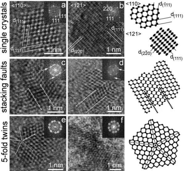
states were obtained for the type 2 diaphite structure with designation (g =3, d =3) that refers to the number of graphitic (g) and diamond (d) layers included in the calculation [27] (Fig. S4). The total electronic density of states was partitioned into contributions from individual atoms. To provide a comparison with the experimental EELS spectra, the Fig. 2. uHRTEM images and FFT patterns for sp3-bonded carbon structures showing stacking faults and twins in diamonds from Orgueil and Murchison meteorites. a) and b) single-crystal 〈110〉and 〈121〉 diamonds and their corresponding structure models shown at right. c) and d) c-h stacking disordered diamonds with their structure models also shown at right. White arrows in the FFT patterns point to streaked reflections. e) and f) cyclic five-fold {111} twins formed within the nanodiamond structures. Dotted lines mark the twin interfaces.
Fig. 3.Hexagonal features from HRTEM data pre- sented in previous reports. a) A six-fold symmetry grain from detonation soot (adapted with permission from [1], Fig. 14a of [1]). The hexagonal features, previously mistakenly attributed to 〈0001〉 lonsda- leite, match the characteristics of type 2 diaphite imaged with ~0.2 nm resolution HRTEM. b) Grain with six-fold symmetry from a detonation produced ND (adapted with permission from [24], Fig. 1a of [24]). The FFT (insert) calculated from the marked regions shows hexagonally arranged reflections with
~0.21 nm spacings. White lines correspond to 0.2 nm-1. Note that the black lines at the edge of grains (marked by black arrows) arise from defocus effects in the image and are not due to structural features.
Diamond & Related Materials 119 (2021) 108573
C 1s state for each individual atom was aligned at zero energy. A shift of +7.5 eV was then applied to correct for a systematic error between the calculated energies of C 1s and 2p levels.
Raman spectra were calculated using DFT for structures with des- ignations (g =5, d =1), (g =3, d =3) and (g =1, d =5) (Fig. 9, Fig. S8).
To obtain Raman intensities using the coupled perturbed Kohn-Sham (CPKS) method [42], full geometry optimizations (lattice parameters and atomic positions) were performed using tighter convergence criteria. The thresholds for the maximum and root mean square (rms) of the forces were set to 0.00015 Ha and 0.0001 Ha, respectively, with the maximum and rms displacements set to 0.00045 Ha and 0.0003 Ha, respectively. The data are presented as orientationally and polarization averaged powder spectra. We note that these calculations do not take
account of electronic effects such as resonance enhancement observed experimentally with different laser excitation wavelengths for graphitic structures [26,43].
3. Results and discussion
3.1. Stacking faults and twins within ND
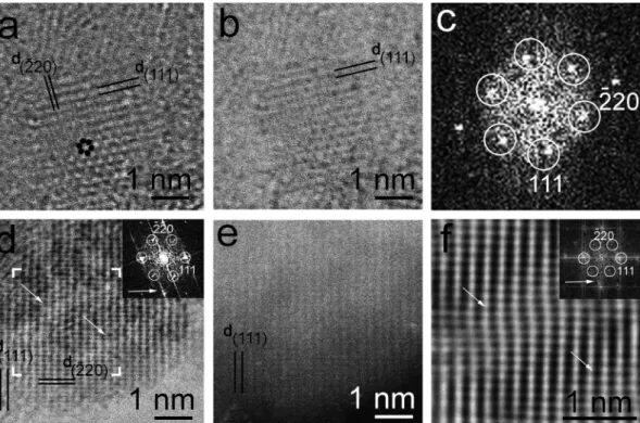
Both the natural and CVD-produced samples studied here revealed features typical of nanocrystalline diamond when imaged at low reso- lution (Fig. 1). A main difference between the natural and CVD NDs is in the respective grain or domain sizes; the natural samples are charac- terized by smaller individual ND grains (1-3 nm) than the ND regions Fig. 4.Grains exhibiting six-fold symmetry reveal the presence of intimately bonded 〈0001〉 graphene units in diamond (Type 2 diaphite). (a) BF and corresponding (b) DF TEM images of a 〈121〉 projected diamond nanocrystal from Orgueil meteorite. (c) FFT calculated from (a) shows hexagonally arranged reflections (outlined by white circles) with ~0.21 nm spacings. Hexagonal rings of C atoms are clearly visible (outlined by black circles in a). (d) BF and corresponding (e) DF images of a
〈121〉 projected individual ND from Murchison meteorite. ~1-nm-wide regions of lighter colour (indicated by white arrows) inclined to (111) diamond planes occur for (d) and give rise to streaking of reflections on the FFT (inset). (f) TEM image calculated with the structure model of type 2 diaphite along 〈121〉 projection shows no evidence for the occurrence of hexagonal rings of graphene but reproduces the image contrast as well as the hexagonally arranged FFT diffraction features of the area marked by white corners in (d).
Fig. 5. BF (a) and corresponding DF (b) images of
〈121〉 (indicated by black arrows) and 〈110〉(indi- cated by white arrows) projected type 2 diaphite from the CVD sample. The outlines of the differently projected grains and the (000l) graphene d- spacings are clearly visible for the DF image. (i) FFT calculated from (i) shows hexagonally arranged (marked by white circles) and graphene (marked by black ar- rows) reflections with ~0.21 nm and ~0.33 nm spacings and indicate 〈121〉 and 〈110〉 oriented nanocrystals, respectively.
P. N´emeth et al.
formed within the synthetic sample (5-7 nm). As mentioned above, uHRTEM images of both grains reveal fringes with 0.206 nm, 0.126 nm, and 0.109 nm corresponding to diamond {111}, {202} and {113} re- flections, respectively, with single crystalline diamond observed only rarely. ND 〈011〉and 〈121〉projections are recognized by the conspic- uous 71◦ cross fringes of {111} diamond spacings and the 90◦ cross fringes of {111} and {220} diamond spacings, respectively (Fig. 2a, b).
Defects are abundant in all grains (Fig. 2c, d). Both stacking faults and {111} cyclic reflection twins, which give rise to grains displaying five- fold (Fig. 2e, f) and eight-fold (Fig. S3) rotation symmetries recog- nized in the diffraction patterns, are commonly observed. Similar cyclic twinning arrangements have been shown to produce pseudo-pentagonal and icosahedral symmetries and external morphologies among laboratory-produced diamonds [44].
3.2. ND grains exhibiting six-fold symmetry patterns
Grains displaying conspicuous hexagonal-fringe patterns with
~0.21 nm spacings and hexagonally arranged reflections in their cor- responding FFT patterns have been recorded in previous HRTEM studies of natural [17] and detonation NDs [1,24] (Fig. 3a,b).
Such hexagonal features have previously been assigned to the 〈0001〉 projection of ordered h-diamond (lonsdaleite) domains. That explana- tion was countered by the analysis of N´emeth et al. [17,45], who used uHRTEM techniques to study key samples and proposed that such pat- terns were in fact formed by two- and four-layer thick {113} cubic diamond twins projected along 〈121〉diamond. However, our DFT cal- culations have now shown that such a 〈121〉 projected {113} diamond twinning pattern is inherently unstable, and that the observed hexagonal
symmetry features arise instead from 〈0001〉 graphene units intergrown with and covalently bonded to the 〈121〉 surfaces of diamond domains, i.
e., type 2 diaphite structures [27–28,31–32,43] (Figs. 4, 5). In the case of the ND (Fig. 4) and CVD (Fig. 5) grains studied here, our fully relaxed DFT calculations indicate that the six-fold symmetry structures and corresponding diffraction patterns that appear throughout the uHRTEM patterns occur due to sp3 diamond regions covalently bonded to graphitic layered units to form coherent interfaces with the surrounding diamond matrix (Fig. 6).
Such nanostructures can be difficult to recognize in uHRTEM images, but their characteristic six-fold diffraction signature is readily apparent in corresponding FFT patterns (Figs. 4, 5). We note that the intensities of the hexagonally arranged reflections may depend on the widths of the graphene units as well as their orientation relative to the viewing di- rection, as discussed below (Fig. 6). In addition, diaphite grains are mixed with single crystalline and defective diamond structures (Fig. 2a- d), and this can cause distortion of the hexagonal symmetry patterns observed in the FFT. This is due to the fact that diamond projected along
〈110〉 gives rise a distorted hexagonal pattern with two sets of {111}, corresponding to ~0.21 nm interlayer spacings, and one set of {002}
diamond fringes, corresponding to ~0.18 nm interlayer spacings (arising due to thickness effects), in which the angle between the cross fringes of {111} diamond is 71◦, whereas between (111) and (002) fringes it is 54◦.
In addition to the challenges associated with obtaining uHRTEM images of NDs and also bulk diamond materials with spatial resolution sufficient to recognize the presence of diaphite nanostructures, addi- tional constraints are introduced by difficulties in recognizing the characteristic features of diaphite directly from the images. These are highlighted by data shown in Fig. 4d. Although the grain shown here is very thin (~ 2-3 nm), the hexagonally arranged C atoms are difficult to distinguish from the surrounding 〈121〉projected diamond. The uHR- TEM image shows ~1-nm-wide white contrast regions (Fig. 4d), while the corresponding FFT reveals streaked hexagonally arranged re- flections (Fig. 4d). The occurrence of the white contrast regions and the invisibility of the hexagonally arranged C atoms are in good agreement with the calculated TEM image, that was developed using a structure model of type 2 diaphite along 〈121〉 projection (Fig. 4f). However, because the CVD grains are larger (~5 nm) than natural NDs (~1-3 nm), the hexagonal features are more clearly visible (Fig. 5). One particularly interesting image from study of the CVD material shows the character- istic interlayer separation of graphene (Fig. 5), corresponding to the
〈110〉 projection of a type 2 diaphite structure (Fig. 6a).
Calculated TEM images based on our structural models demonstrate that the characteristic few-layered graphene units of type 2 diaphite and the six-fold symmetry are only observed along specific viewing di- rections, i.e., with grains appropriately oriented with respect to the electron beam. The six-fold symmetry features of diaphite become replaced by the distorted hexagonal features of diamond as the grains are rotated out of the preferred orientation (Fig. 6a-h).
3.3. ND grains and regions with regular and distorted twelve-fold symmetry
Some grains within the meteoritic ND residues and domains in the CVD-produced samples exhibit complex uHRTEM images and their corresponding FFTs reveal twelve spots with 0.21 nm spacings (Fig. 7).
FFTs with twelve diffraction spots arranged in a symmetrical 6 × 2 pattern indicating slightly distorted twelve-fold symmetry are also observed (Fig. 7h). uHRTEM images displaying regular twelve-fold rotational symmetry evidenced by FFTs have all twelve ~0.21 nm re- flections rotated by 30◦with respect to each other (Fig. 7e-g). One such image had previously proposed to be assigned to twelve {113} twin domains [17], but that interpretation is unlikely because of the inherent instability of such 〈121〉 projected {113} twin structures [27]. The twelve-fold rotation represents a crystallographically forbidden Fig. 6. Interpretation of grains with six-fold symmetry in terms of type 2 dia-
phite nanostructures. (a-d) DFT relaxed models of type 2 diaphite nano- structures consisting of three diamond and three graphene (d =3, g =3) units viewed in different projections with their corresponding (e-g) calculated uHRTEM images. At the top (a-d) are shown the type 2 diaphite structural motifs along various observation directions. The corresponding calculated TEM images (e-g) illustrate the challenge for recognizing the characteristic graphene units in diaphite nanostructures with randomly oriented projections along the viewing axis. Although (a) and (b) are both 〈110〉 projected type 2 diaphite structures, the graphene interlayer spacing is barely visible for (e) only and is hidden for (f). Similarly, although hexagonally arranged C atoms are clearly observed for (c and g) they are invisible for (d and h).
Diamond & Related Materials 119 (2021) 108573
symmetry element, but it can be generated by the orientationally directed bonding of the sp3 diamond matrix around the type 2 diaphite core structures (Fig. 7i). In particular, such arrangements have been reported for “twisted” bilayer graphene [46–47]. The relative rotation of graphene sheets gives rise to FFTs with 2 ×6, i.e., ideally 12, equally spaced graphene diffraction spots. Ideally, the rotation is 30◦, but arbitrary rotation about 30-60◦angles between the graphene sheets has also been reported [47]. Since the appearance of the twisted graphene layers on diffraction patterns are identical to the arrangements and d- spacings of the reflections we observe on FFTs for some ND grains (Fig. 7a-h), we suggest that the observed regular and distorted twelve- fold rotational symmetry arises from the rotation of stacked graphene units in type 2 diaphite nanostructures (Fig. 7i-j).
3.4. Explaining the unusual but characteristic pre-edge EELS features of NDs
The C K edge EELS of NDs show pre-edge features that are not ex- pected to occur for bulk diamond at 282.5 (A), 284.7 (B) and 286.5 (C) eV, with a further shoulder appearing on the main diamond edge at 287.8 eV (D) [23–24] (Fig. 8a). We used DFT methods to calculate the unoccupied p-projected electronic density of states (UDOS) for a representative type 2 diaphite structure containing graphene and dia- mond (designation: g =3, d =3) units [27] (Fig. 8b-c, Figs. S4-S6).
These calculations led to a semi-quantitative understanding of the un- occupied states and gave insights into the origin of the additional C K
edge spectral features [23–24] (Fig. 8a). Core-loss edges are dominated by transitions from a core level to localized, site-specific, symmetry- projected, UDOS. For carbon, the C K edge spectral features are domi- nated by C 1s transitions to UDOS states with p-like character. The total UDOS in our calculations was partitioned into contributions from the individual atoms (Fig. 8b-c, Figs. S4-S6), showing that the Fermi level for the sp2 region is contained within the gap of the sp3 matrix. We note that part of the calculated atom-projected DOS for the interface atoms bonding between the sp2 graphene units and the sp3 domains straddles the Fermi level, raising interesting possibilities for localized electronic conduction. The contribution from the occupied states has been removed from the DOS shown in Fig. 8a. The sp2-sp3 interface causes a misalignment of the C-1s states, by up to 1 eV, with the core levels for the sp2 atoms at higher and those of the sp3 atoms at lower energies. In- spection of the calculated electron density patterns shows that the shift is due to partial polarity of the interfacial sp2-sp3 bonds. Because of the local nature of electronic transitions measured in EELS, the UDOS atomic projections were realigned such that the zero of the energy for each atom coincides with its C1s core state (Fig. S5): this alignment demonstrates the influence of the sp2-sp3 interface on the energy levels (Fig. 8c) and the result matches well with measured EELS spectra (Fig. 8a). The shift to higher energy of the C1s states for the sp2 interface atoms reduces their separation from the conduction band states, and causes appearance of the low-energy EELS feature A. We thus assign the weak A feature to carbon atoms at the sp2-sp3-bonded interface. The B and C features are transitions associated with the graphene-like layers at Fig. 7. uHRTEM images and FFT patterns of nanodiamonds exhibiting both regular and distorted twelve-fold symmetry compared with model diaphite structures.
Grains from Orgueil (a), Murchison (b and c) and a laboratory produced CVD sample (d) and their corresponding FFTs (e-h). White lines correspond to 0.2 nm-1. White and black circles indicate two lattices with hexagonally arranged reflections (compare with Fig. 4a, b). The twelve-fold symmetry of (c) is distorted on the image (marked by white arrow) as well as on FFT (h). (i) Structure model of two vertically stacked graphene units (“twisted” graphene) rotated by 30◦respect to each other gives rise to twelve-fold rotational symmetry. (j) FFT of the model structure (i) shows reflections arranged according to perfect twelve-fold rotation. 20◦
“twisted” rotation of two graphene units results in an image (k) and corresponding FFT (l) with distorted symmetry, which are similar to the observation (c) and (h).
Grey lines on panels (i) and (k) mark 0.21 nm spacings.
P. N´emeth et al.
the core of the diaphite domains. Taking the feature D at 287.8 eV as the onset of the conduction band for diamond, bands B and C occur within the diamond band gap, while in a perfect sp3 lattice the pre-edge peak A at 282.5 eV would be located below the Fermi level. Its presence in the ND EELS spectra requires modification of the electronic structure beyond that associated with a point defect.
We note that other interpretations for the additional EELS peaks have also been proposed. For example, the B and C peaks have been assigned to fullerene-like structures on the ND surface [24]. Although these have been reported to occur among other shocked samples [48], no such structures were observed in our HRTEM studies of meteoritic NDs. It is important to note that the dark features occurring at the edge of the NDs, that has been used as evidence to suggest the existence of fullerene/
graphene structures [24], can be confused with the effect of defocusing an HRTEM image (see black arrows in Figs. 1c and 4b). It is also known that NDs must be decorated with C–H groups to achieve valence satu- ration, accompanied by some surface structural relaxation [20,24].
Oxygenated surface defects could also give rise to additional EELS pre- peaks with similar energy loss values [49–50]. However, the charac- teristic 288 eV feature of -COOH species is absent from our results, and EELS data from a cluster of 2-5 nm NDs showed a barely detectable signal at the O1s position (Fig. S2). It has also recently been suggested that peak A, which occurs below the Fermi level for diamond (282.8 eV), can be assigned to three-coordinated carbon atoms around vacancy (V) sites associated with nitrogen-vacancy (N–V) centres [24]. Although this remains a possible alternative interpretation for this peak, our ND EELS results indicate only 0.5-1.4 at.% N present within the samples studied (Fig. S2), which is too low to result in a distinct accompanying C1s peak. Previous experimental and simulation studies have shown that
the probability of forming a significant concentration of N–V defects is low for 2-5 nm NDs [51].
3.5. Raman spectroscopic signatures associated with the presence of diaphite domains within NDs
Raman spectroscopy is a well-established technique for character- ization of carbon materials, and several reports of its application to natural and synthetic NDs have appeared in the literature, but the results are not fully explained. Most studies carried out using blue-green (514.5, 488 nm) to UV (325, 245 nm) laser excitation show spectra that are dominated by broad bands between 1550 and 1620 cm-1, while the expected peak near 1332 cm-1 due to crystalline diamond is often significantly lowered in intensity or even absent, as shown by others [7,15,25–26,43] and also in our results (Fig. 9, Fig. S7). This result is surprising, even taking into account that the sp3-bonded features can be broadened, shifted in position and develop marked asymmetry due to the nanosized domains combined with the presence of hexagonal stacking sequences within the diamond material [52–54].
The features at higher wavenumber occur beyond the available vibrational density of states (vDOS) for sp3-bonded diamond structures and are typically assigned to the “G” band of sp2-bonded domains within graphitic or amorphous carbon structures [15–16,26,43]. It could be suggested that such sp2-bonded material might have been incompletely removed by acid digestion from the original sample, or was developed as layers surrounding the ND particles. However, as we discuss below, the Raman features assigned to sp2-bonded structures within the ND sam- ples studied here do not correspond to those expected for typical graphitic materials. Additional broad “D” bands appearing between Fig. 8. EELS spectra of nanodiamonds compared with calculated data based on type 2 diaphite nanostructures. (a) Unusual pre-edge EELS features (A: 282.5 eV, B:
284.7 eV, C: 286.4 eV, D: 287.8 eV) of Murchison nanodiamond in comparison to ordinary diamond and graphite. b) and c) Local atomic structure and atom- projected unoccupied electronic density of states (UDOS) with p-type symmetry of the (g =3, d =3) diaphite structure (Fig. S4). b) Local structure of the dia- phite interface, colour-coded to show atoms composing the sp2 ‘bulk’ (graphene) region, the sp2 ‘interface’ atoms, sp3 atoms at the interface in highly-distorted tetrahedral geometry and sp3 ‘bulk’ (diamond) atoms. c) Atom-projected unoccupied electronic density of states for the selected atoms indicated in b), with the C 1s core states aligned at zero energy, to provide a comparison with the experimental EELS spectra. Complete atom-projected unoccupied electronic density of states functions for the diaphite structure (Fig. S4) are provided in Figs. S5-6.
Diamond & Related Materials 119 (2021) 108573
1300 and 1330 cm-1 for graphitic structures as they become disordered and Raman selection rules are relaxed [26], and this can interfere with the structural interpretation of bands assigned to the sp3-bonded ma- terial. In particular, it is well known that the intensity of the “G” and “D” band features of graphitic carbonaceous materials is greatly enhanced due to electron-phonon coupling and resonant effects that vary with Raman excitation wavelength across the visible-UV range [26,43].
However, it is also important to note that the intrinsic Raman cross- section of sp2-bonded structures is significantly greater than that of diamond-structured materials, independent of resonance enhancement effects. Previous researchers have estimated that the main graphitic Raman feature is between 25 and 200 times more intense than that of diamond based on experimental data [15,26,55,56]. Our DFT results presented below that do not consider any electron-phonon or resonant enhancement effects are in agreement with this estimate, indicating that the matrix elements responsible for the Raman scattered intensity of the characteristic C-C stretching vibrations are several hundred times greater for sp2- compared with sp3-bonded structures (Fig. 9, Fig. S8).
Early ND studies were carried out for “diamond-like” films contain- ing ~10 nm domains prepared by CVD [15]. The Raman spectra were unusual in that they contained three broad bands and additional peaks or shoulders occurring across the 1100-1600 cm-1 region. The authors noted that the two strongest features at 1590 and 1355 cm-1 were similar to the vibrational modes for graphite and diamond, although they ruled out the presence of a micron-scale composite of the two phases [15].
Nemanich et al. [15] did identify a small sharp peak at 1332 cm-1 due to the presence of crystallites of cubic diamond within some samples. The authors concluded that the CVD “nanodiamond” films contained some regions with macroscopic diamond that included within or were sur- rounded by amorphous or at least poorly crystalline sp2-bonded graphitic material. Such signatures of “bulk” diamond are often observed in the Raman spectra of shocked meteoritic and detonation diamond samples [7,15,25–26,43]. Their absence for our samples in- dicates (a) that any regions representing large volumes of well- crystallized diamond are not present in the ND materials examined, and (b) that the Raman data obtained with excitation wavelengths spanning the near-IR to visible ranges were dominated by signatures from sp2-bonded regions included within the cubic-hexagonal stacking structures of the diamond matrix (Fig. 9). Nemanich et al. also noted an unexplained band at ~1140 cm-1 [15]. Such a feature has been assigned to the presence of trans-polyacetylene structures within the ND sample [26], although such an assignment has been questioned for CVD samples [57].
Our Raman studies of a CVD ND film provided by R. Nemanich using visible (488, 514 nm) laser excitation showed a similar range of spectral features to those predicted by our DFT calculations for type 2 diaphite structures containing d =3, g =3 layers (Fig. 9, Figs. S7, S8). When excited by 785 nm laser radiation, both Murchison ND and CVD dia- mond samples are dominated by a broad asymmetric band at 1280-1290 cm-1, that can be assigned to C-C stretching vibrations within sp3- bonded c-h stacked diamond layers [52–54]. Such a main Raman signal is also predicted by our DFT calculations for diaphite structures (Fig. 9, Figs. S7, S8). In the case of Murchison, the featureless asymmetric Raman band extending between ~1000-1450 cm-1 could encompass the range expected for disordered c-h stacked sp3-bonded nanostructures [27,5 2-54]. The 785 nm spectrum for CVD ND also exhibits a clear shoulder near 1200 cm-1 that can be attributed to the presence of h- stacked units within the structure [54,55]. However, a second obvious shoulder near 1600 cm-1 is difficult to interpret on the basis of purely sp3-bonded structures. Features in both these regions are predicted to occur for type 2 diaphite structures (Fig. 9, Figs. S7, S8).
The Raman results obtained using blue-green (514.5, 488 nm) ra- diation are surprisingly different, for both samples. The CVD ND mate- rial exhibits a pattern showing clear maxima near 1200, 1300 and 1600 cm-1, with the highest wavenumber feature exhibiting two components near 1510 and 1640 cm-1. The Murchison sample exhibits a similar pattern for visible excitation, that is clearly different to the 785 nm spectrum (Fig. 9). The weakest feature at lowest frequency could be assigned to nanocrystalline diamond regions, although the fact that its wavenumber appears to shift with excitation wavelength is unexpected for purely sp3-bonded structures. However, such shifts due to resonant interactions might be expected for diaphite nanostructures, in which the sp2- and sp3- domains are coherently bonded together and there are cooperative electronic interactions at the graphitic-diamond interface, as revealed by our EELS experiments and DFT calculations (see Section 3.6 above). The higher frequency bands observed in the 1500-1600 cm-1 range are typically associated with graphitic (sp2-bonded) structures, and are predicted to occur for type 2 diaphite structures (Fig. 9).
Using 785 nm radiation, we observed an additional band near 820 cm-1 for the Murchison sample, that is not observed for any known graphitic or diamond structures, but is predicted by our DFT calculations for type 2 diaphite (Fig. 9). A feature near 1140 cm-1 is also predicted by our DFT results. As noted above, a peak at this wavenumber has been associated with trans-polyacetylene (tPA) structural units in CVD dia- mond samples [26], although that interpretation has been challenged [57]. There is no clear evidence for this feature in any of our spectra, although our Murchison sample with 488 nm excitation does show a very weak “bump” near this position. However, the meteoritic material is not expected to contain any significant contribution from tPA units.
We now address the unexpected and remarkable differences in relative intensity patterns observed for the Raman bands excited with Fig. 9. Raman spectra obtained for Murchison ND aggregates for samples as
shown in Fig. 1a compared with DFT calculated Raman spectra for d =3, g =3 diaphite (Fig. S8). The experimental spectra show broad features with relative intensities that depend on the excitation wavelength. Spectra obtained with a 785 nm laser (red) are dominated by a broad asymmetric band with maximum near 1200 cm-1 that can be assigned to sp3-bonded vibrations of a cubic- hexagonal layered diamond structure. With blue-green (514 and 488 nm) excitation, the main features are typically assigned to “G” and “D” bands of disordered graphitic structures. However, the main peak positions do not correspond to either of these “ideal” solutions. In addition the second order features between 2700 and 3000 cm-1 do not agree in their positions or relative intensities with those for disordered bulk graphite, few-layered graphene or c-h layer disordered diamond materials (Fig. S7). (For interpretation of the refer- ences to colour in this figure legend, the reader is referred to the web version of this article.)
P. N´emeth et al.
near-IR vs visible wavelengths. It is well known that semimetallic sp3- bonded structures exhibit strong electron-phonon interactions that result in resonance enhancement of their characteristic Raman modes along with dispersion of their wavenumber values according to the excitation wavelength [26,43]. Such intensity enhancement and dispersion characteristics are not available to wide-gap diamond struc- tured materials. Typically, the signal from sp3-bonded units is enhanced as the excitation wavelength is lowered. However, we observe the opposite behaviour for our ND samples that we suggest is associated with the unusual electronic structures developed within the sp2- and sp3- bonded diaphite nanostructures and at the interface between the two.
We must also consider the relative Raman response from sp2- and sp3-bonded structures in the absence of resonance enhancement. It has been estimated from experimental studies (that obviously include the excitation wavelength) that graphitic structures have matrix elements for Raman activity that are 20-200 times that of sp3-bonded structures [15,54,55]. Our DFT calculations for diaphite structures with different g/d ratios generally agree with this estimate (Fig. S8). We also note that
“normal” graphitic or graphene structures exhibit characteristic well- defined and strong second-order Raman signatures in the 2500-3100 cm-1 range [26,43]. However, we note that for defective graphitic ma- terials, the second order peaks are often broadened and reduced in in- tensity. These signals are notably absent or are significantly broadened, and shifted to uncharacteristically low wavenumbers for our spectra (Fig. 9, Fig. S7).
3.6. Significance of the presence of diaphite structures within NDs It has already been noted that the presence of diaphite structures within a diamond matrix can improve the mechanical resistance by increasing both the compressive and tensile strength of the sp3-sp2 bonded nanocomposite material [28,31–32,58]. We suggest that this improvement contributes to the remarkable qualities of NDs for abrasive applications and to the superior protection afforded to surfaces by CVD films. Further applications are suggested by our analysis of the elec- tronic properties of the incorporated graphene layers and their coher- ently bonded interfaces with the sp3 domains. These could lead to opportunities for conducting graphene-based nanostructures embedded within the wide-gap semiconducting diamond host with external con- tacts potentially created by laser waveguide channelling [59]. The presence of diaphite domains influences the local geometry and orga- nisation of the surrounding sp3-bonded layers due to the need to maintain coherent covalent bonding across the sp2-sp3 interface. That results in the unusual 6- and 12-fold symmetries observed in uHRTEM images and FFT diffraction figures discussed above. In our study, we examined >100 grains from Murchison, Orgueil and CVD nano- diamonds and observed these symmetry features in ~5% of the grains.
However, because of orientational effects relative to the HRTEM viewing direction noted above, the diaphite nanostructures are likely to be present in much larger concentration throughout the sample. Each 2- 3 nm ND grain is estimated to contain ~1000-2000 atoms [60]. Because only a small proportion of graphitic units is needed to direct the relative stacking of a much larger number of sp3-bonded layers extending around the diaphite core, these nanostructures can be thought to play an essential role in determining the internal structure of NDs. An energy- volume map showing the stability of diaphite nanostructures with different extents of the sp3- and sp2-bonded (g and d) domains existing across the phase space between diamond and graphite/graphene was presented previously [27–28]. The diaphite structures can be considered to form a polysomatic mineral series, similar to that seen in biopyribole minerals, that contain structural units ranging between single and double/multiple-chain silicate units to extended mica sheets [61]. We suggest that the diaphite structures similarly constitute a new class of elemental carbon materials.
4. Conclusions
In this work we report a new interpretation of ND structures based on our observation of unusual six- and twelve-fold symmetry objects within natural meteorite samples and laboratory-produced materials obtained by CVD. These remarkable structural features were first recognized by detailed analysis of uHRTEM images of materials that are typically described as “nanodiamond”. These symmetries cannot appear within fully sp3-bonded diamond structures, even considering twinning pat- terns available to cubic- and hexagonally-stacked layer arrangements.
The unusual symmetry objects are found to be ubiquitous among the large selection of ND grains and CVD crystalline domains studied here, and they reveal the presence and possibly widespread existence of a new class of diaphite-structured nanocarbons. Following structural models supported by DFT calculations, we suggest that the existence of diaphite core structures could explain the spectroscopic, TEM imaging and diffraction results of meteoritic and synthetic NDs. The diaphite nano- structured materials correspond to neither pure graphite nor diamond phases, and recognizing their presence now helps us understand the unique EELS and Raman data of NDs. We suggest that they may have been observed in previous studies of natural and synthetic ND samples, but have remained unidentified because of the challenges associated with the observation and interpretation of their characteristic features.
The presence of the diaphite nanostructures can be associated with the remarkable material properties that are observed or could be engineered for synthetic samples.
CRediT authorship contribution statement
P.N., L.A.J.G., K.M. and P.F.M. together initiated and coordinated different aspects of the project. P.N. and L.A.J.G. were involved in the HRTEM investigation, data analysis and interpretation. L.A.J.G. ob- tained the high-resolution EELS data. C.A.H. and P.F.M. performed the Raman measurements, analysis and interpretation. K.M. carried out the DFT calculations and modelling of type 2 diaphite and K.M., F.C. and C.
J.P. carried out the DOS calculations and interpretation of the EELS spectra. M.M. performed microbeam XRD scanning experiments and C.
G.S and R.L.S. simulated the HRTEM images. P.N. and P.F.M. led anal- ysis of the results and manuscript writing and figures were prepared by P.N., K.M., L.A.J.G. and C.G.S. All authors participated in discussion of the results and their interpretation and have given approval to the final version of the manuscript.
Declaration of competing interest
The authors declare that they have no known competing financial interests or personal relationships that could have appeared to influence the work reported in this paper.
Acknowledgements
We are grateful to the staff and for use of the facilities in the John M.
Cowley Center for High Resolution Electron Microscopy at Arizona State University (USA). P.N. acknowledges financial support from the Hun- garian National Research, Development and Innovation Office project NKFIH_KH126502, the J´anos Bolyai Research Scholarship and the ÚNKP-20-5-PE-7 New National Excellence Program of the Ministry for Innovation and Technology. L.A.J.G. was supported by a NASA Emerging Worlds grant NNX17AE56G. P.F.M., C.A.H. and F.C. received funding from the EU Graphene Flagship under Horizon 2020 Research and Innovation program grant agreement nos. 785219-GrapheneCore2 and 881603-GrapheneCore3. R.L.S. received a DTP studentship from the UCL department of Chemistry. This work made use of the ARCHER UK National Supercomputing Service (http://www.archer.ac.uk) via K.M.
and F.C.'s membership of the UK's HEC Materials Chemistry Consortium, which is funded by EPSRC (EP/L000202). K.M. and F.C. gratefully
Diamond & Related Materials 119 (2021) 108573 acknowledge HPC resources provided by the UK Materials and Molec-
ular Modelling Hub, which is partially funded by EPSRC (EP/P020194/
1), and UCL Grace and Kathleen HPC Facilities and associated support services, in completion of this work. C.J.P. is supported by the EPSRC through Grant No. EP/P022596/1. The authors acknowledge the Euro- pean Synchrotron Radiation Facility for provision of synchrotron beamtime at the beamline ID27.
Appendix A. Supplementary data
Supplementary data to this article can be found online at https://doi.
org/10.1016/j.diamond.2021.108573.
References
[1] T.L. Daulton, D.D. Eisenhour, T.J. Bernatowicz, R.S. Lewis, P.R. Buseck, Genesis of presolar diamonds: comparative high-resolution transmission electron microscopy study of meteoritic and terrestrial nano-diamonds, Geochim. Cosmochim. Acta 60 (1996) 4853–4872. https://www.sciencedirect.com/science/article/pii/S00167 03796002232?via%3Dihub.
[2] G. Huss, Meteoritic nanodiamonds: messengers from the stars, Elements 1 (2) (2005) 97–100. https://pubs.geoscienceworld.org/msa/elements/article-abstract/
1/2/97/137577/Meteoritic-Nanodiamonds-Messengers-from-the-Stars?red irectedFrom=fulltext.
[3] G.K. Ustinova, Production of anomalous Xe in nanodiamond in chondrites during the last supernova explosion predating the origin of the solar system, Geochem. Int.
49 (2011) 555–567. https://link.springer.com/article/10.1134/S0016702 911060103.
[4] J.A. Viecelli, S. Bastea, J.N. Glosli, F.H. Ree, Phase transformations of nanometer size carbon particles in shocked hydrocarbons and explosives, J. Chem. Phys. 115 (2001) 2730, https://doi.org/10.1063/1.1386418.
[5] G.W. Yang, J.B. Wang, Q.X. Liu, Preparation of nano-crystalline diamonds using pulsed laser induced reactive quenching, J. Phys. Condens. Mat. 10 (1998) 7923–7927, https://doi.org/10.1088/0953-8984/10/35/024.
[6] J.-P. Boudou, P.A. Curni, F. Jelezko, J. Wrachtrup, G. Balasubramanian, R. Reuter, P. Aubert, M. Sennour, A. Thorel, E. Gaffet, High yield fabrication of fluorescent nanodiamonds, Nanotechnology 20 (2009), 235602, https://doi.org/10.1088/
0957-4484/20/23/235602.
[7] V.N. Mochalin, O. Shenderova, D. Ho, Y. Gogotsi, The properties and applications of nanodiamonds, Nat. Nanotechnol. 7 (1) (2012) 11–23, https://doi.org/10.1038/
nnano.2011.209.
[8] M. Ivanov, O. Shenderova, Nanodiamond-based nanolubricants for motor oils, Curr. Opin. Solid State Mater. Sci. 21 (1) (2017) 17–24. https://www.sciencedirec t.com/science/article/pii/S1359028616301097.
[9] A.M. Schrand, S.A.C. Hens, O.A. Shenderova, Nanodiamond particles: properties and perspectives for bioapplications, Crit. Rev. Solid State Mater. Sci. 34 (2009) 18–74. https://www.tandfonline.com/doi/abs/10.1080/10408430902831987?jo urnalCode=bsms20.
[10] A.S. Barnard, Predicting the impact of structural diversity on the performance of nanodiamond drug carriers, Nanoscale 10 (19) (2018) 8893–8910. https://pubs.
rsc.org/en/content/articlelanding/2018/nr/c8nr01688g#!divAbstract.
[11] V.Y. Osipov, F. Treussart, S.A. Zargaleh, K. Takai, F.M. Shakhov, B.T. Hogan, A. Baldycheva, Photoluminescence from NV- centres in 5 nm detonation nanodiamonds: identification and high sensitivity to magnetic field, Nanoscale Res.
Lett. 14 (2019) 279. https://nanoscalereslett.springeropen.com/articles/10.1186/
s11671-019-3111-y.
[12] F. Brandenburg, R. Nagumo, K. Saichi, K. Tahara, T. Iwasaki, M. Hatano, F. Jelezko, R. Igarashi, T. Yatsui, Improving the electron spin properties of nitrogen-vacancy centres in nanodiamonds by near-field etching, Sci. Rep. 8 (2018) 15847. https://www.nature.com/articles/s41598-018-34158-4.
[13] M. Gulka, H. Salehi, B. Varga, E. Middendorp, O. Pall, H. Raabova, T. Cloitre, F.J.
G. Cuisinier, P. Cigler, M. Nesladek, Cs. Gergely., Simultaneous label-free live imaging of cell nucleus and luminescent nanodiamonds, Sci. Rep. 10 (2020) 9791.
https://www.nature.com/articles/s41598-020-66593-7.
[14] A.A. Shiryaev, J.A. Hinks, N.A. Marks, G. Greaves, F.J. Valencia, S.E. Donnelly, R.
I. Gonz´alez, M. Kiwi, A.L. Trigub, E.M. Bringa, J.L. Fogg, I.I. Vlasov, Ion implantation in nanodiamonds: size effect and energy dependence, Sci. Rep. 8 (1) (2018) 5099, https://doi.org/10.1038/s41598-018-23434-y.
[15] R.J. Nemanich, J.T. Glass, G. Lucovsky, R.E. Shroder, Raman scattering characterization of carbon bonding in diamond and diamondlike thin films, J. Vac.
Sci. Technol. A 6 (1988) 1783–1787. https://avs.scitation.org/doi/10.1116/
1.575297.
[16] R.J. Nemanich, J. Carlisle, A. Hirata, K. Haenen, CVD diamond—research, applications, and challenges, MRS Bull. 39 (6) (2014) 490–494. https://www.ca mbridge.org/core/journals/mrs-bulletin/article/cvd-diamondresearch-application s-and-challenges/259CD6D3BA75F89755E5AC12EB0EB05F.
[17] P. N´emeth, L.A.J. Garvie, P.R. Buseck, Twinning of cubic diamond explains reported nanodiamond polymorphs, Sci. Rep. 5 (2015) 18381, https://doi.org/
10.1038/srep18381.
[18] S. Bhargava, H.D. Bist, S. Sahli, M. Aslam, H.B. Tripathi, Diamond polytypes in the chemical-vapor-deposited diamond films, Appl. Phys. Lett. 67 (12) (1995) 1706–1708. https://aip.scitation.org/doi/10.1063/1.115023.
[19] J.M. Cowley, R.C. Mani, R.M.K. Sunkara, M. O’Keeffe, C. Bonneau, Structures of carbon nanocrystals, Chem. Mater. 16 (2004) 4905–4911. https://pubs.acs.org/
doi/abs/10.1021/cm0491429.
[20] A.S. Barnard, M. Sternberg, Crystallinity and surface electrostatics in diamond nanoparticles, J. Mater. Chem. 17 (2007) 4811–4819. https://pubs.rsc.
org/en/content/articlelanding/2007/jm/b710189a/unauth#!divAbstract.
[21] A.S. Barnard, G. Opletal, S.L.Z. Chang, Does twinning impact structure/property relationships in diamond nanoparticles? J. Phys. Chem. C 123 (2019) 11207–11215. https://pubs.acs.org/doi/10.1021/acs.jpcc.9b00142.
[22] Sh. Michelson, A. Hoffman, Hydrogen in nano-diamond films, Diam. Relat.
Materials. 14 (2005) 470–475. https://www.sciencedirect.com/science/article/
pii/S0925963505000166.
[23] L.A.J. Garvie, Surface electronic structure of meteoritic nanodiamonds, Meteorit.
Planet. Sci. 41 (2006) 667–672. https://onlinelibrary.wiley.com/doi/abs/10.1111 /j.1945-5100.2006.tb00982.x.
[24] S.L.Y. Chang, A.S. Barnard, C. Dwyer, C.B. Boothroyd, R.K. Hocking, E. Osawa, R.
J. Nicholls, Counting vacancies and nitrogen-vacancy centers in detonation nanodiamond, Nanoscale 8 (2016) 10548–10552. https://pubs.rsc.
org/en/content/articlelanding/2016/nr/c6nr01888b#!divAbstract.
[25] A.A. Shiryaev, A.V. Fisenko, I.I. Vlasov, L.F. Semjonova, P. Nagel, S. Schupple, Spectroscopic study of impurities and associated defects in nanodiamonds from efremovka (CV3) and orgueil (CI) meteorites, Geochim. Cosmochim. Acta 75 (2011) 3155–3165. https://www.sciencedirect.com/science/article/pii/S0016703 711001487.
[26] A.C. Ferrari, J. Robertson, Raman spectroscopy of amorphous, nanostructured, diamond-like carbon, and nanodiamond, Philos. Trans. R. Soc. A 362 (2004) 2477–2512. https://royalsocietypublishing.org/doi/10.1098/rsta.2004.1452.
[27] P. N´emeth, K. McColl, R.L. Smith, M. Murri, L.A.J. Garvie, M. Alvaro, B. P´ecz, A.
P. Jones, F. Cor`a, C.G. Salzmann, P.F. McMillan, Diamond-graphene composite nanostructures, Nano Lett. 5 (2020) 3611–3619. https://pubs.acs.org/doi /10.1021/acs.nanolett.0c00556.
[28] P. N´emeth, P.K. McColl, L.A.J. Garvie, C.G. Salzmann, M. Murri, P.F. McMillan, Complex nanostructures in diamond, Nat. Mater. 19 (2020) 1126–1131, https://
doi.org/10.1038/s41563-020-0759-8.
[29] H. Ohnishi, K. Nasu, K., Generation and growth of sp3-bonded domains by visible photon irradiation of graphite, Phys. Rev. B: Condens. Matter Mater. Phys. 80 (2009), 014112. https://journals.aps.org/prb/abstract/10.1103/PhysRevB.80.
014112.
[30] J. Kanasaki, E. Inami, K. Tanimura, H. Ohnishi, K. Nasu, Formation of sp3-bonded carbon nanostructures by femtosecond laser excitation of graphite, Phys. Rev. Lett.
102 (2009), 087402. https://journals.aps.org/prl/abstract/10.1103/Phy sRevLett.102.087402.
[31] S. Zhang, Q. Zhang, Z. Liu, D. Legut, T.C. Germann, S. Veprek, H. Zhang, R. Zhang, Ultrastrong p-bonded interface as ductile plastic flow channel in nanostructured diamond, ACS Appl. Mater. Interfaces 12 (3) (2020) 4135–4142. https://pubs.acs.
org/doi/10.1021/acsami.9b19725.
[32] Q. Zhang, C. Wanga, H. Zhang, S. Zhang, Z. Liu, D. Legut, S. Veprek, R. Zhang, Designing ultrahard nanostructured diamond through internal defects and interface engineering at different length scales, Carbon 170 (2020) 394–402.
https://www.sciencedirect.com/science/article/pii/S0008622320308010.
[33] C. Prescher, V.B. Prakapenka, DIOPTAS: a program for reduction of two- dimensional X-ray diffraction data and data exploration, High Press. Res 35 (3) (2015) 223–230. https://www.tandfonline.com/doi/abs/10.1080/08957959.201 5.1059835.
[34] J.L. L´ab´ar, Electron diffraction based analysis of phase fractions and texture in nanocrystalline thin film, part I: principles, Microsc. Microanal. 14 (2008) 287–295. https://www.cambridge.org/core/journals/microscopy-and-microana lysis/article/abs/electron-diffraction-based-analysis-of-phase-fractions-and-textur e-in-nanocrystalline-thin-films-part-i-principles/
B5D7456CC66291441CF7BF1DAF4A5CA7.
[35] A. G´omez-Rodríguez, L.M. Beltr´an-del-Río, R. Herrera-Becerra, SimulaTEM:
multislice simulations for general objects, Ultramicroscopy 110 (2010) 95–104.
https://www.sciencedirect.com/science/article/pii/S030439910900206X.
[36] Y. Jiang, Z. Chen, Y. Han, P. Deb, H. Gao, S. Xie, P. Purohit, M.W. Tate, J. Park, S.
M. Gruner, V. Elser, D.A. Muller, Electron ptychography of 2D materials to deep sub-ångstrom resolution, Nature 559 (2018) 343–349, https://doi.org/10.1038/ ¨ s41586-018-0298-5.
[37] R. Dovesi, A. Erba, R. Orlando, C.M. Zicovich-Wilson, B. Civalleri, L. Maschio, M. R´erat, S. Casassa, J. Baima, S. Salustro, B. Kirtman, Quantum-mechanical condensed matter simulations with CRYSTAL, Wiley Interdiscip. Rev. Comput.
Mol. Sci. 8 (2018) 1–36. https://onlinelibrary.wiley.com/doi/10.1002/
wcms.1360.
[38] H.J. Monkhorst, J.D. Pack, Special points for Brillouin-zone integrations, Phys.
Rev. B 13 (1976) 5188. https://journals.aps.org/prb/abstract/10.1103/PhysRev B.13.5188.
[39] S. Grimme, J. Antony, S. Ehrlich, H. Krieg H., A consistent and accurate ab initio parametrization of density functional dispersion correction (DFT-D) for the 94 elements H-Pu, J. Chem. Phys. 132 (2010), 154104. https://aip.scitation.org/doi/
10.1063/1.3382344.
[40] S. Grimme, S. Ehrlich, L. Goerigk, Effect of the damping function in dispersion corrected density functional theory, J. Comput. Chem. 32 (2011) 1456–1465.
https://onlinelibrary.wiley.com/doi/full/10.1002/jcc.21759.
[41] S. Grimme, A. Hansen, J.G. Brandenburg, C. Bannwarth, Dispersion-corrected meanfield electronic structure methods, Chem. Rev. 116 (2016) 5105–5154.
https://pubs.acs.org/doi/abs/10.1021/acs.chemrev.5b00533.
P. N´emeth et al.