www.small-journal.com
Patterning of Nanoparticle-Based Aerogels and Xerogels by Inkjet Printing
Franziska Lübkemann, Jan Frederick Miethe, Frank Steinbach, Pascal Rusch, Anja Schlosser, Dániel Zámbó, Thea Heinemeyer, Dominik Natke, Dorian Zok, Dirk Dorfs, and Nadja C. Bigall*
F. Lübkemann, J. F. Miethe, F. Steinbach, P. Rusch, A. Schlosser, Dr. D. Zámbó, T. Heinemeyer, D. Natke, D. Zok,
Dr. D. Dorfs, Prof. N. C. Bigall
Institute of Physical Chemistry and Electrochemistry Leibniz Universität Hannover
30167 Hannover, Germany
E-mail: nadja.bigall@pci.uni-hannover.de
F. Lübkemann, J. F. Miethe, P. Rusch, A. Schlosser, Dr. D. Zámbó, T. Heinemeyer, D. Natke, D. Zok, Dr. D. Dorfs, Prof. N. C. Bigall
Laboratory of Nano and Quantum Engineering Leibniz Universität Hannover
30167 Hannover, Germany
The ORCID identification number(s) for the author(s) of this article can be found under https://doi.org/10.1002/smll.201902186.
DOI: 10.1002/smll.201902186
1. Introduction
One key challenge for a technical and economical mastering of fields like sensors, energy harvesting, and components for elec- tronic devices is to develop upscalable and automatized procedures for the production of metal and semiconductor based thin-film coated electrode surfaces. Inkjet printing is a novel technique to deposit nanocrystals (NCs) on different surfaces, e.g. conducting foils, conducting glasses, electrodes, and many more. In contrast to conventional techniques (dip-coating, spin-coating, spray-coating)
Nanoparticle-based voluminous 3D networks with low densities are a unique class of materials and are commonly known as aerogels. Due to the high surface-to-volume ratio, aerogels and xerogels might be suitable materials for applications in different fields, e.g. photocatalysis, catalysis, or sensing. One major difficulty in the handling of nanoparticle-based aerogels and xerogels is the defined patterning of these structures on different substrates and surfaces. The automated manufacturing of nanoparticle-based aerogel- or xerogel-coated electrodes can easily be realized via inkjet printing. The main focus of this work is the implementation of the standard nanoparticle-based gelation process in a commercial inkjet printing system. By simultaneously printing semiconductor nanoparticles and a destabilization agent, a 3D network on a conducting and transparent surface is obtained. First spectro- electrochemical measurements are recorded to investigate the charge–carrier mobility within these 3D semiconductor-based xerogel networks.
Inkjet Printing
the inkjet printing process exhibits benefits of faster manufacturability, a lower material to sample casualty rate, and the production of defined areas with less coating material.
Plenty of scientists are using inkjet printing for the deposition of metal NCs[1–3] or semi- conductor NCs[4–9] to manufacture struc- tured electronic components for chip design and sensing.[6,10–12] In addition, some works on laser induced 3D printing for the fabrica- tion of porous materials can be found.[13,14]
Semiconductor NCs are of high interest, since the interconnection of crystal size, and shape and the opto electronic pro perties defined by the quantum confinement effects diversifies the field of obtainable systems.[15]
The main motivation for this work is inves- tigating aqueous semiconductor based nanoinks regarding the possibility to build up 3D porous networks in-situ during the printing process. Since the development of nanoparticle based aerogel structures,[16–19]
there is a high interest in these self-assembled 3D nanoparticle networks and in exploiting their suitability in different fields, e.g.
photo catalysis,[20–22] electrocatalysis,[23,24] and photo-electrochem- ical application like sensing.[12,25] By controlling the destabilization process of the nanocrystals, it is possible to obtain nanoparticle networks in which the nanoparticles are connected to each other in a defined way.[26–32] Nevertheless, there is a lack of possible tech- niques for forming these highly porous 3D aerogels into defined macroscopic shapes and patterns on conducting surfaces to make them suitable for spectro-electrochemical measurements or sensing application.
Here, we present the automatized manufacturing of porous 3D networks (also known as aerogels and xerogels) on conducting electrode surfaces via inkjet printing. Based on previous works on inkjet printing[9] and nanoparticle based gela- tion[26] we chose CdSe/CdS dot-in-rod shaped semiconductor heterostructures as building blocks. The standard gelation process is implemented by using a commercial office printer to simultaneously print the CdSe/CdS nanorod (NR) building blocks and the destabilization agent (H2O2) on conducting tin-doped-indium oxide (ITO) coated glass surfaces (Figure 1).
Due to this “gelation via inkjet printing” method, short GelVIP, porous 3D CdSe/CdS gel network-coated films can be obtained.
By drying the hydrogel under ambient conditions xerogels with a less porous network can be obtained, whereas by drying under supercritical CO2 conditions aerogels with a highly porous network are obtained. The photo-electrochemical pro- perties of the automatically manufactured 3D CdSe/CdS NR
© 2019 The Authors. Published by WILEY-VCH Verlag GmbH & Co.
KGaA, Weinheim. This is an open access article under the terms of the Creative Commons Attribution-NonCommercial License, which permits use, distribution and reproduction in any medium, provided the original work is properly cited and is not used for commercial purposes.
xerogel networks on electrode surfaces were measured to eluci- date charge carrier mobilities within the interconnected CdSe/
CdS NR networks, which lead to a deeper understanding of the charge carrier movement/diffusion within such a porous semiconductor gel structure. Therefore, we compared photo- electrochemical measurement data of the xerogel materials to those of simple submonolayers and multilayers of the nanopar- ticle building blocks. In future, the precise deposition of nano- particle-based xerogel-coated films via inkjet printing might enable the possibility to create small area patterned electrodes with several xerogels of different materials. Due to the flexibility of the inkjet printing method, the use of various semiconduc- tors with different band gap energies during the printing pro- cess would give the opportunity to built-up a multifunctional sensor consisting of different xerogel networks.
2. Results and Discussion
2.1. Printing of Different 3D Semiconductor Networks
The combination of the gelation process and the deposition of nanoparticles via inkjet printing enables the patterning of 3D highly porous semiconductor nanorod-based networks on con- ducting surfaces (Figure 1). The aqueous CdSe/CdS nanorod- based ink was prepared based on our previous work.[9,33,34] In the first step, the mixing ratio between the nanorods and the destabilization agent as well as the resulting gelation time have to be adjusted to the inkjet printing conditions, which are com- pletely different than the original solution-based synthesis route
destabilization agent, here H2O2, the mixing ratio of nanoparti- cles and destabilization agent, the concentration of nanorods in the aqueous nanoink, and the repetition of printing cycles the optimal ratio between homogeneity and coverage of the printed films was investigated (Figures S1–S3, Supporting Informa- tion). Morphological changes in the xerogel-coated films due to the variation of the mixing ratio of the nanoparticles and the destabilization agent were analyzed by scanning electron microscopy (SEM; Figure S4, Supporting Information). SEM images demonstrate that low amount of destabilization agent (mixing ratio of nanoink to H2O2 1 : 0.2) leads to a more com- pact or rather dense film with nearly the same morphology like a only nanoink coated film (Figure 2a). It can be anticipated that the oxidation of the surface ligands plays a crucial role in the formation of the assembled nanoparticle network, hence, the lower amount of H2O2 leads to the incomplete destabiliza- tion process and therefore the gel formation cannot take place.
By increasing the amount of destabilization agent (mixing ratio of nanoink to H2O2 1 : 0.4) it can be seen, that the porosity of the film increases prominently. However, further increase of the destabilization agent amount (mixing ratio of nanoink to H2O2 1:0.5) also leads to a dense and compact structure of the printed film. In this case, the high amount of destabilization agent oxidizes too many ligands on the nanoparticle surfaces, which manifest itself in a fast precipitation of the nanoparti- cles. Based on all parameter variations, the optimal printing parameters for our system were determined and are given in the Experimental Section. After the adjustment of the printing system, the nanorod-based network structures can be printed by in-situ formation of a hydrogel. Various drying methodolo- gies can be followed after the printing process to achieve dry printed nanorod networks. First, to obtain xerogel networks the film was printed under ambient conditions and was dried in a humidity chamber (73% of relative humidity) at ambient conditions. Due to capillary forces that occur during the drying as well as the printing process, the network contracts and is relatively compact compared to an aerogel network. Second, to achieve an aerogel network, a Kistler's method of supercritical drying must be applied.[35] To obtain aerogel films and to avoid drying in the meantime of the printing process, it is necessary to print and store the hydrogel film under humid conditions (73% of relative humidity). Afterward, certain steps after the printing process are necessary to obtain the aerogel structure.
Primarily, the water inside the pore system must be exchanged to acetone. The exchange was performed via Soxhlet extraction.
By using a critical point drying system, the acetone phase can be exchanged to liquid CO2 followed by supercritical drying.
The received aerogel networks show nearly no loss in volume Figure 1. Gelation via inkjet printing (GelVIP) process. Schematic illus-
tration of the cartridges and the printing process for automatized manu- facturing of 3D semiconductor network coated electrodes.
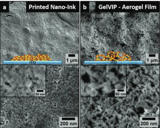
compared to the respective solvogels/hydrogels. To investigate the morphology and porosity of 3D printed network films, porous 3D CdSe/CdS NR network-coated films were printed and converted to both aerogels and xerogels. As comparison for the increase in porosity an identically treated film of CdSe/CdS NRs without the addition of the destabilization agent during the printing process was also printed. Figure 2 shows SEM images of a CdSe/CdS NR film (Figure 2a) printed in the absence of any destabilizing agent and a 3D NR based aerogel network film (Figure 2b). In the SEM images (Figure 2a) of the nanoink-only printed NR film, a compact solid film with some cracks due to the drying process is visible. On higher magnification images (see also the inset) single NRs that are arranged side by side can be recognized. Within the nanoink-only printed CdSe/CdS NR film no direct crystal–crystal contact is present which leads to a partial detaching of the coated film in solutions. Caused by low stability of the nongelated film no subsequent washing steps were possible (since their washing results in destruction of the film) resulting in the presence of KOH crystals pre- cipitated upon solvent evaporation. By simultaneous printing of the nanorods and the destabilization agent, the assembly of the NRs in 3D networks on the electrode can be achieved.
Figure 2b illustrates SEM images of a 3D CdSe/CdS aerogel network film fabricated by gelation via inkjet printing (GelVIP).
In the higher magnification images an obvious increase of the porosity of the obtained printed structure can be seen. Here, in the SEM images CdSe/CdS NR building blocks within the porous structure are visible. By adding destabilization agent
to the printing process, an NR assembly with tip-to-tip contact between the single NRs is obtained, which was already shown in our previous work about the gelation of CdSe/CdS NRs (without printing).[26] Within the printed structure some NRs are assembled side by side while others are contacted at the tips of the NRs. These particle–particle connections lead to a large increase in the stability of the printed aerogel and xerogel films.
Comparative TEM micrographs of the nanoink-only and CdSe/
CdS aerogel printed film are shown in Figure S5 (Supporting Information). Compared to the pure printed CdSe/CdS NR film a 3D, highly porous CdSe/CdS NR based network was printed.
If we compare SEM images of the printed CdSe/CdS aerogel and CdSe/CdS aerogel gelated in a vessel, the morphology and porosity of the whole printed 3D nanoparticle based structure is more compact or rather dense (Figure S6, Supporting Infor- mation). This behavior can be explained by four different rea- sons: i) to achieve thick films various repetitions of the printing cycles have to be performed, which leads to a merging of the structure, ii) the permanent movement of the printing support after each printing cycle breaks some of the looser particle con- nections, (iii) gelation and aging time are drastically reduced, which results in a faster and less controlled network forma- tion, and iiii) capillary forces due to drying in the meantime of printing process can also lead to a shrinkage of the nano- particle-based network. Nevertheless, the porosity and nanorod- assembly morphology clearly resemble those of an aerogel. As mentioned before, CdSe/CdS xerogel networks can be fabri- cated likewise (related SEM images; see Figure S7, Supporting Figure 2. SEM images of simply printed CdSe/CdS NR nanoink-only film and 3D CdSe/CdS NR based aerogel network film (100 printing cycles) by
“GelVIP” technique. a) Schematic illustration and SEM images of dense printed CdSe/CdS nanorod film on conducting ITO substrate. b) Schematic illustration and SEM images of highly porous printed CdSe/CdS nanorod-based aerogel network on conducting ITO substrate.
400 cycles the film thickness can be increased, and the overall film coverage becomes denser. Spectroscopic measurements were performed in order to investigate the optical proper- ties of the nanoparticle-based xerogel films and whether the CdSe/CdS NRs are affected by the mechanical stress due to the printing process (see Figure S8 of the Supporting Infor- mation and the following text). Photographic images (insets Figure 3) taken under ambient and UV light illumination indicate an increase in the film's optical density by increasing the number of printing cycles. Scanning electron microscopy allows us to determine the particular film morphology (see top view micrographs Figure 3, top) and the film thickness (see cross-section micrographs Figure 3, bottom). All micrographs taken from top show a porous gel structure with a rough sur- face independent of the number of printing cycles. The SEM micrograph of gels obtained after 25 printing cycles (Figure 3a, top) shows areas within the film with low amounts of CdSe/
CdS xerogel network. The micrographs of 100 printing cycles (Figure 3b, top) and 400 printing cycles (Figure 3c, top) indi- cate an increase in film homogeneity due to the increase of extensively coated areas within the film. By recording cross-section micrographs (Figure 3, bottom), the film thick- nesses of the three different printed CdSe/CdS xerogel sub- strates can be evaluated. The film thickness is increasing with increasing number of printing cycles. However, likely due to local thickness deviations, a linear relation between the film thickness and the applied number of printing cycles was not observed. By subsequently printing 25 cycles a film thickness of 250–380 nm (Figure 3a, bottom), with 100 printing cycles a thickness of 1.2–2.2 µm (Figure 3b, bottom) and by printing 400 cycles a thickness of 2.8–4.4 µm (Figure 3c, bottom) is obtained. By evaluating the whole cross-section of the printed films, the average thickness of the printed xerogel films with their deviations can be determined as 308 nm ± 60 nm for 25 printing cycles, 1.57 µm ± 0.44 µm for 100 printing cycles, and 2.56 µm ± 0.86 µm for 400 printing cycles (Figure 3d and Figure S9, Supporting Information). The variation of the film thickness within each single film can be caused by different factors: i) lower viscosity of nanoparticle-based ink compared to commercially available color inks, which affects formation, falling, and wetting of the ink droplet, ii) movement of printing support between the repetitions of the printing cycles benefits flowing of the solution and accumulation at particular places, and iii) irregular silane functionalization can promote the accu- mulation at particular places.
By printing five cycles of a quick response code (QR code) consisting of a CdSe/CdS NR xerogel network on soda lime glass, we want to demonstrate the success of printing defined
patterns. Figure 4 shows photographs of the printed QR code taken under ambient light (Figure 4, left) and UV light (Figure 4, right) irradiation. The resolution of the printed QR code is 285 dpi. At this resolution, the single squares and rec- tangles of the QR code exhibit sharp edges and no coalescence of adjacent regions is visible that ensures the suitable read- ability. An increase of the resolution leads to coalescence of the single points of the printed pattern. The functionality of the Figure 3. SEM images from top view (top) and cross-section view (bottom) of CdSe/CdS xerogel substrates with different thicknesses. a) 25 printing cycles. b) 100 printing cycles. c) 400 printing cycles. Insets show photographs taken under ambient light irradiation (left) and UV light irradiation (right) of 0.9 × 0.9 cm printed squares. d) measured average thickness (50 points) and standard deviation of different printing cycles.
All measurement data are shown in Figure S9 (Supporting Information).
printed QR code was proven by successful scans with commer- cial QR code scanners running on different operating systems.
2.3. Photo-Electrochemical Measurements on Xerogel-Coated Electrodes
The main aim of our photo-electrochemical analysis of the printed nanorod xerogel network-coated electrodes is to reveal the correlation of the electric properties of the material and the geometrical organization of the assembled nanorods in the gel network. By illuminating the CdSe/CdS xerogel photons can be absorbed, which excite electrons from the valence band to the conduction band whereby positively charged holes remain in the valence band. Due to the particle–particle connection within the 3D CdSe/CdS xerogel network the electrons are supposed to travel within the whole nanorod network, whereas the holes remain in the CdSe core regions (scheme of band structure;
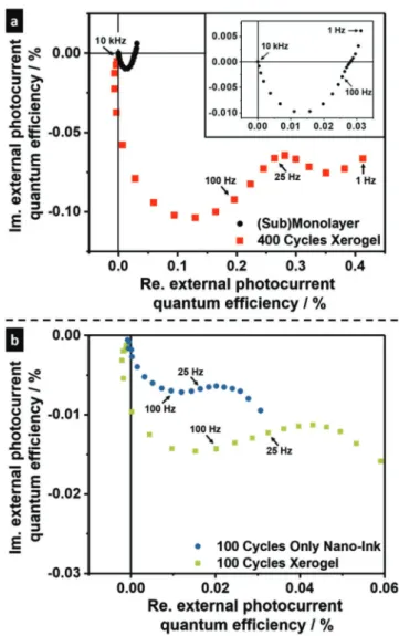
see Figure S10, Supporting Information) as observed spectro- scopically for aerogel systems from the same nanorods.[15] The CdSe/CdS xerogel network-coated photoelectrode produced via GelVIP, printed CdSe/CdS nanoink-only films and a (sub) monolayer of the nanorods coated photoelectrode were charac- terized by means of intensity modulated photocurrent spectros- copy (IMPS). By recording intensity modulated photocurrent spectra the charge carrier transport within the different nanorod assemblies can be investigated. All measurements were carried out in a self-built measurement cell,[36] and the on-off frequency of the LED (468 nm, 525 nm) is varied from 10 kHz to 1 Hz. For the measurements a 0.5 m solution of Na2SO3 was used, which operates as a hole scavenger. The IMPS response of the (sub) monolayer and the hydrated 400 cycle printed CdSe/CdS xerogel network-coated electrode (5 d electrolyte exposure) are displayed in Figure 5a. The Nyquist complex plane plot[37,38] of the CdSe/
CdS NR (sub)monolayer coated electrode (black circles) shows only one semicircle in the applied frequency range (10 kHz to 1 Hz). In case of the via GelVIP produced xerogel coated photo- electrode (400 cycles, red squares, film thickness 2.56 ± 0.86 µm) one semicircle in the frequency range of 1 kHz to 25 Hz, and a second semicircle in the frequency range between 25 and 1 Hz can be observed. The higher frequency semicircle (10 kHz to 100 Hz for (sub)monolayer electrode, 10 kHz to 25 Hz for the via GelVIP produced photoelectrode) is widely known to
be based on the transfer of trapped charge carriers across the particle–electrolyte and the particle–electrode interface.[37,39]
The semicircle at lower excitation frequencies (25 to 1 Hz for xerogel coated electrode) is based on the charge transport across the nanoparticle network.[40,41] Moreover, IMPS spectros- copy of 100 printing cycles produced films of printed CdSe/
CdS nanoink only (blue circles, film thickness 1 µm ± 0.24 µm) and CdSe/CdS xerogel network (green squares) were con- ducted. Here, a 525 nm LED was used for illumination, which leads to an increase in the penetration depth in the printed films and provides more information about the charge carrier mobility within the xerogel structure. Due to the printing set- tings (different printed volumes, see the Experimental Section) Figure 4. Photographs of printed QR code consisting of a porous nanorod
xerogel network (5 printing cycles) under ambient light (left) and UV light (right) illumination. The resolution of the printed QR code is 285 dpi.
Figure 5. Intensity modulated photocurrent spectra of a printed CdSe/
CdS xerogel network, a printed CdSe/CdS nanoink-only, and a CdSe/CdS NR (sub)monolayer coated electrode. a) IMPS response of CdSe/CdS (sub)monolayer (black circles, inset show magnification) and printed and hydrated CdSe/CdS xerogel network (400 printing cycles, red squares).
b) IMPS response of a printed CdSe/CdS nanoink-only (100 printing cycles, blue circles) and a printed CdSe/CdS xerogel network coated elec- trode (100 printing cycles, green squares). The spectra were measured under 468 nm (IMPS response, panel a) and 525 nm (IMPS response, panel b) LED illumination with frequencies from 10 kHz to 1 Hz at a bias potential of 150 mV (vs Ag/AgCl).
plane plot of both coated films, one semicircle in the higher fre- quency range (1 kHz to 25 Hz) can be observed, which is here also related to the transfer of trapped charge carriers across the particle–electrolyte or particle–electrode interface. The radius of the high frequency semicircle of the xerogel film (green squares) is larger than of the nongelated film (blue circles), so that the afore-mentioned processes are more efficient in case of the xerogel film. This observation can possibly be linked to the oxidation of the surface ligands during the gelation pro- cess, which not only results in the formation of direct particle–
particle contacts but also in an enhanced electrolyte accessibility of the particle surface due to the lower surface ligand coverage.
These two effects moreover increase the charge carrier transfer within the gelated xerogel film, as it is reflected in the appear- ance of a second semicircle at lower frequencies. Interestingly, also the nongelated film shows a small second semicircle in the low frequency region. We attribute this observation to the slow drying process of the printed electrodes, during which the NRs can assemble side by side so that charge carrier transport between some NRs can occur. Nevertheless, the contribution of charge carrier transport processes to the photocurrent is much more prominent for the CdSe/CdS xerogel network-coated elec- trodes than for the nongelated ones. In addition, an increase in the photocurrent with increasing electrolyte exposure time was observed solely for the gelated xerogel films. We assume that the dense xerogel films slowly rehydrate by electrolyte diffu- sion into the structures under retention of the particle–particle contacts (more insights into the mechanism will be given in a future work).
In conclusion, the presence of the second semicircle in the lower frequency region for the printed CdSe/CdS xerogel network films (100 cycles, 400 cycles) proves the existence of (stable) interconnections between the NRs within the 3D nano- particle-based networks, since it is indicating that the electron indeed is able to travel within the gels produced via GelVIP.
3. Conclusion
In conclusion, we have successfully developed a new approach for an automatized fabrication of 3D nanorod-based networks via inkjet printing, the so-called “gelation via inkjet printing”
short “GelVIP.” As far as it is known, it is the first report about inkjet printing of nanoparticle-based aero- and xerogel net- works. It was shown that the implementation of the gelation in the printing process results in the successful fabrication of porous 3D networks. Therefore, an aqueous nanoink consisting of CdSe/CdS NRs was simultaneously printed with H2O2 as
functional patterning. Due to this work, it will be possible in future to fabricate various different kinds of aerogel-like highly porous nanoparticle-based network-coated electrodes, with pos- sible applications in, e.g., photo-electrochemical and electro- chemical sensing, photo-electrocatalysis, and optoelectronics.
4. Experimental Section
Reagents and Materials: Cadmium oxide (CdO, 99.99%) and selenium (Se, 99.99%) were purchased from Alfa Aesar. Tri-n-octylphosphine oxide (TOPO, 99%) and tri-n-octylphosphine (TOP, 97%) were purchased from ABCR. Hexylphosphonic acid (HPA, ≥ 99%) and octadecylphosphonic acid (ODPA, ≥ 99%) were purchased from PCI synthesis. Hydrogen peroxide (H2O2, 35%), (3-mercaptopropyl)trimethoxysilane (MPTMS, 95%), 1-Octadecene (ODE, 90%), sodium sulfite (≥ 98%), and sulfur (S, 99.98%) were purchased from Sigma Aldrich. Methanol (≥ 99.5%) and toluene (99.9%) were purchased from Carl Roth. Substrate: Tin- doped indium oxide glass (ITO glass) 1.1 mm coated unpolished soda lime float glass, VisionTek, 12 ohms/sq. As commercial inkjet printer, an Epson Expression Premium XP-620 was used.
Synthesis of CdSe Dots: CdSe dots were synthesized by using a slightly modified and six times scaled up procedure developed by Carbone et al.[34] 0.36 g CdO, 18 g TOPO, and 1.7 g ODPA were placed in a 50 mL three neck flask. The mixture was heated up to 150 °C under vacuum and degassed for 1 h. Subsequently, the reaction mixture was heated up to 300 °C under an argon atmosphere, and 10.8 mL TOP was injected.
The temperature was increased to 380 °C to obtain a clear solution.
Then, 10.8 mL TOP:Se (4.4 mmol) solution was quickly injected into the reaction mixture. The temperature recovered before quenching with 6 mL ODE. After cooling the reaction mixture, 25 mL toluene was added at 70 °C and the CdSe dots were precipitated by the addition of 25 mL methanol. The solution was centrifuged for 10 min (3885 RCF).
The solution was purified by the addition of toluene/methanol and centrifugation twice. The CdSe dots were stored in toluene.
Synthesis of Dot-in-Rod CdSe/CdS NRs: The CdS shell growth was adapted from Carbone et al.[34] In an eight times scaled up synthesis, 0.48 g CdO, 24 g TOPO, 2.32 g ODPA, and 0.64 g HPA were placed in a 100 mL three neck flask, heated up to 150 °C and degassed for 1 h.
Subsequently, the temperature was increased to 300 °C under an argon atmosphere, and 12 mL TOP was injected followed by increasing the temperature to 380 °C. At that temperature 14.4 mL TOP:S (2.21 mmol) containing 200 × 10−6m of CdSe dots (concentration was determined by UV/Vis spectroscopy and calculation according the work of Yu et al.[42]) were quickly injected and the reaction mixture was further heated for 8 min. After cooling the reaction mixture, 25 mL toluene was added at 70 °C and the CdSe/CdS NRs were precipitated by the addition of 25 mL methanol. The solution was centrifuged for 10 min (3885 RCF). The NR solution was washed twice by the addition of toluene/methanol and eventually stored in toluene.
Phase Transfer to Aqueous Solutions: To obtain an aqueous CdSe/
CdS NR solution, a phase transfer according to the procedure of Kodanek et al. was performed.[33] 3 mL of the organic CdSe/CdS NRs (c(Cd) = 128 mmol L−1) were precipitated with methanol, centrifuged,
and redissolved in 3 mL n-hexane. A second phase of 10 mL methanol, 0.2 g KOH, and 0.24 mL MPA was added to the CdSe/CdS NR solution and both were shaken overnight. The polar phase was separated, centrifuged, and the CdSe/CdS NRs were stored in 12 mL 0.1 m KOH solution.
Preparation of ITO Slides: The ITO glass slides were cut into pieces of ≈1 × 6 cm and cleaned for 2.5 h at 70 °C with a mixture of 1:1:5 volume parts of hydrogen peroxide (35%): ammonium hydroxide (25%): deionized water. Afterward the slides were rinsed with water and dried under an airflow. For the functionalization, the activated slides were placed in a solution containing 150 mL toluene and 1.5 mL (3-mercaptopropyl)trimethoxysilane for 18 h at 70 °C. Afterward the slides were rinsed with water and dried under an airflow.
Inkjet Printing of CdSe/CdS Nanorod-Based Networks on ITO Glass:
We adapted the printing system from our previous work with distinct adjustments to print 3D CdSe/CdS NR based networks on ITO glass.[9]
The concentration of the destabilization agent (H2O2, 0.35 wt% and 0.5 wt%), the mixing ratio of nanorods and destabilization agent (1 : 0.05 to 1 : 0.5), the concentration of the aqueous nanoink (c(Cd) = 8.15 to 32 mmol L−1), and repetition of printing cycles was varied to find the optimal printing conditions. To print 3D nanoparticle-based networks, aqueous CdSe/CdS NR based nanoink (c(Cd) = 32 mmol L−1) was filled into the magenta cartridge, and the 0.35 wt% destabilization H2O2 solution was filled into the cyan cartridge. By the supplied software CD Print the print area (0.9 cm × 0.9 cm, resolution 150 dpi) was programmed. The composition was controlled by using the CYMK color code. For destabilization of CdSe/CdS NR films the printed color was adjusted to 100% magenta. For the CdSe/CdS hydrogels the printed color was programmed to 70% magenta and 30% of cyan (1 : 0.4). By varying the number of repetitions of printing cycles (25, 100, 400 printing cycles), the thickness was controlled. To obtain an aerogel-coated sample and avoid drying of the hydrogel films while the printing process, the whole printing process was done under humid conditions (73%).
All other printing experiments were done under ambient conditions.
After printing the CdSe/CdS NR hydrogel coated substrates were placed in an environmental chamber with a humidity of 73% (saturated saline solution). For initializing the gelation, the environmental chamber was placed in an oven for 1 min at 80 °C. Afterward the substrates were slowly dried, with intermediate washing steps, in the environmental chamber under ambient conditions. For aerogel coated film preparation the aqueous phase was replaced by acetone phase via soxhlet extraction with subsequent supercritical drying.
Preparation of CdSe/CdS NR (sub)Monolayer-Coated Electrode: The preparation of CdSe/CdS (sub)monolayer coated electrode was adapted from our previous work.[36] The MPTMS functionalized ITO coated glass was immersed in 10 mL of a toluene solution containing CdSe/
CdS nanorods (c(Cd) = 15 mmol L−1) and shaken for 24 h with a velocity of 250 rpm. Then, the slide was rinsed with fresh toluene to remove unbounded nanorods and dried under ambient conditions.
Scanning Electron Microscopy: The film morphology and thickness were investigated by SEM using a JEOL JSM 6700F microscope equipped with a cold field emission gun source. The glass substrates were fixed with a carbon badge on the brass holder and treated at the edges with silver conductive paint to increase the conductivity.
Transmission Electron Microscopy: The morphology of the printed films was investigated by TEM using an FEI Tecnai G2 F20 TMP (CS = 2 mm, CC = 2 mm), equipped with a 200 kV field emission gun.
The micrographs were taken in bright-field mode. For grid preparation of the printed films, the carbon–coated copper grid was pressed on the top of the films to detach some parts of the printed films.
Spectroscopy Characterization: UV/Vis absorption spectra of the solution and the printed films were recorded using an Agilent Cary 500 absorption spectrometer equipped with an Agilent DRA-2500 integrating sphere. Fluorescence spectra were measured in a Fluoromax-4 from Horiba. The absorption and fluorescence spectra of the solution were measured in a 1 cm quartz cuvette diluting 10 µL sample in 3 mL toluene.
Atomic Absorption Spectroscopy (AAS): The Cd concentration of the aqueous NR solution was determined by AAS using a Varian AA140
instrument supplied with an air/acetylene (1.5:3.5) flame atomizer.
The samples here were prepared by dissolving defined amounts of CdSe/CdS NRs in aqua regia and diluting them in 50 mL volumetric flasks. Additionally, five Cd2+ solutions with known concentrations were measured to obtain a calibration curve.
Electrochemical Measurements (Intensity Modulated Photocurrent Spectra): The applied electrochemical setup was based on a ModuLab XM ECS Potentiostat from Solatron. All shown measurements were realized under application of a three electrode setup based on the 3D CdSe/CdS NR network-coated working electrodes (or nanorod (sub)monolayer coated electrode), Ag/AgCl reference electrodes purchased from BASi and a platinum wire as a counter electrode. For all measurements an aqueous solution of 0.5 m Na2SO3 (pH = 9.6) was applied as an electrolyte since it is shown in literature that Na2SO3 is an effective hole scavenger in case of metal-calcogenide materials.[43,44] In order to measure IMPS spectra of the (sub)monolayer and 400 printing cycles CdSe/CdS NR xerogel-coated electrode a 468 nm LED was applied. In case of the 100 printing cycles- coated CdSe/CdS NR nanoink-only and CdSe/CdS xerogel-coated electrode a 525 nm LED was used. By using 525 nm instead of the 468 nm LED the penetration depth of the light is increased, which leads to more information of the charge carrier movement within the films. The film thicknesses of the measured samples are 800 nm–1.4 µm for 100 printing cycles of CdSe/CdS nanoink-only. The utilization of a 7270 Dual reference Lock-In amplifier purchased from Signal Recovery made an effective recording of the IMPS possible. A scheme of such a setup is given in different literature sources.[36,44] The obtained data were evaluated with the software Acquire.
The spectra were measured under illumination (468 and 525 nm) with on-off frequencies from 10 kHz to 1 Hz at a bias potential of 150 mV.
Supporting Information
Supporting Information is available from the Wiley Online Library or from the author.
Acknowledgements
The authors (N.C.B., F.L., J.F.M.) are grateful for financial support from the German Federal Ministry of Education and Research (BMBF) within the framework of the program NanoMatFutur, support code 03X5525.
Furthermore, the project leading to these results has in part received funding from the European Research Council (ERC) under the European Union’s Horizon 2020 research and innovation program (grant agreement No.
714429). The authors (D.D. and F.L.) are grateful for the financial support from Volkswagen foundation (lower Saxony/Israel cooperation, Grant ZN2916). The author D.D. thanks the DFG (research Grant 1580/5-1).
The author N.C.B. thanks the DFG (research Grant BI 1708/4-1). The project has in parts been funded by the Deutsche Forschungsgemeinschaft (DFG, German Research Foundation) under Germany’s Excellence Strategy within the Cluster of Excellence PhoenixD (EXC 2122). The author A.S. thanks the Hannover school of nanotechnology for financial support. The authors thank Prof. Caro and Prof. Feldhoff for access to a scanning electron microscope and the Laboratory of Nano and Quantum Engineering for support.
Conflict of Interest
The authors declare no conflict of interest.
Keywords
aerogels, gelation via inkjet printing, inkjet printing, semiconductor nanoparticles, xerogels
Received: April 30, 2019 Revised: June 30, 2019 Published online: August 8, 2019
Adv. Mater. 2007, 19, 3574.
[7] S. Halivni, S. Shemesh, N. Waiskopf, Y. Vinetsky, S. Magdassi, U. Banin, Nanoscale 2015, 7, 19193.
[8] C. Ingrosso, J. Y. Kim, E. Binetti, V. Fakhfouri, M. Striccoli, A. Agostiano, M. L. Curri, J. Brugger, Microelectron. Eng. 2009, 86, 1124.
[9] F. Lübkemann, R. Anselmann, T. Kodanek, N. C. Bigall, Chem. Ing.
Tech. 2017, 89, 807.
[10] R. Esfandyarpour, M. J. DiDonato, Y. Yang, N. G. Durmus, J. S. Harris, R. W. Davis, Proc. Natl. Acad. Sci. USA 2017, 114, E1306.
[11] Q. Shen, X. Zhao, S. Zhou, W. Hou, J. J. Zhu, J. Phys. Chem. C 2011, 115, 17958.
[12] A. Schlosser, L. C. Meyer, F. Lübkemann, J. F. Miethe, N. C. Bigall, Phys. Chem. Chem. Phys. 2019, 21, 9002.
[13] S. Saeed, R. M. Al-Sobaihi, M. F. Bertino, L. S. White, K. M. Saoud, J. Mater. Chem. A 2015, 3, 17606.
[14] A. A. Pawar, S. Halivni, N. Waiskopf, Y. Ben-Shahar, M. Soreni- Harari, S. Bergbreiter, U. Banin, S. Magdassi, Nano Lett. 2017, 17, 4497.
[15] J. Zhao, M. A. Holmes, F. E. Osterloh, ACS Nano 2013, 7, 4316.
[16] T. Gacoin, L. Malier, J.-P. Boilot, J. Mater. Chem. 1997, 7, 859.
[17] T. Gacoin, K. Lahlil, P. Larregaray, J. P. Boilot, J. Phys. Chem. B 2001, 105, 10228.
[18] T. Gacoin, L. Malier, J. P. Boilot, Chem. Mater. 1997, 9, 1502.
[19] B. Capoen, T. Gacoin, J. M. Nédélec, S. Turrell, M. Bouazaoui, J.
Mater. Sci. 2001, 36, 2565.
[20] J. Puskelova, L. Baia, A. Vulpoi, M. Baia, M. Antoniadou, V. Dracopoulos, E. Stathatos, K. Gabor, Z. Pap, V. Danciu, P. Lianos, Chem. Eng. J. 2014, 242, 96.
[21] A. Freytag, C. Günnemann, S. Naskar, S. Hamid, F. Lübkemann, D. Bahnemann, N. C. Bigall, ACS Appl. Nano Mater. 2018, 1, 6123.
[22] L. Korala, J. R. Germain, E. Chen, I. R. Pala, D. Li, S. L. Brock, Inorg.
Chem. Front. 2017, 4, 1451.
M. Colombo, G. Pugliese, J. Poppe, C. Demirci, I. Kretschmer, D. W. Bahnemann, P. Behrens, N. C. Bigall, Angew. Chem., Int. Ed.
2016, 55, 1200.
[29] J. L. Mohanan, I. U. Arachchige, S. L. Brock, Science 2005, 307, 393.
[30] N. C. Bigall, A.-K. Herrmann, M. Vogel, M. Rose, P. Simon, W. Carrillo-Cabrera, D. Dorfs, S. Kaskel, N. Gaponik, A. Eychmüller, Angew. Chem., Int. Ed. 2009, 48, 9731.
[31] V. Lesnyak, S. V. Voitekhovich, P. N. Gaponik, N. Gaponik, A. Eychmüller, Am. Chem. Soc. Nano 2010, 4, 4090.
[32] G. Zeng, N. Shi, M. Hess, X. Chen, W. Cheng, T. Fan, M. Niederberger, ACS Nano 2015, 9, 4227.
[33] T. Kodanek, H. M. Banbela, S. Naskar, P. Adel, N. C. Bigall, D. Dorfs, Nanoscale 2015, 7, 19300.
[34] L. Carbone, C. Nobile, M. De Giorgi, F. Della Sala, G. Morello, P. Pompa, M. Hytch, E. Snoeck, A. Fiore, I. R. Franchini, M. Nadasan, A. F. Silvestre, L. Chiodo, S. Kudera, R. Cingolani, R. Krahne, L. Manna, Nano Lett. 2007, 7, 2942.
[35] S. S. Kistler, Nature 1931, 127, 741.
[36] J. F. Miethe, F. Lübkemann, J. Poppe, F. Steinbach, D. Dorfs, N. C. Bigall, ChemElectroChem 2018, 5, 175.
[37] L. M. Peter, J. Li, R. Peat, H. J. Lewerenz, J. Stumper, Electrochim.
Acta 1990, 35, 1657.
[38] H. Nyquist, Bell Syst. Tech. J. 1932, 11, 126.
[39] E. P. A. M. Bakkers, A. L. Roest, A. W. Marsman, L. W. Jenneskens, L. I. de Jong-van Steensel, J. J. Kelly, D. Vanmaekelbergh, J. Phys.
Chem. B 2000, 104, 7266.
[40] X. Mao, R. Zhou, S. Zhang, L. Ding, L. Wan, S. Qin, Z. Chen, J. Xu, S. Miao, Sci. Rep. 2016, 6, 19390.
[41] E. Guillén, F. J. Ramos, J. A. Anta, S. Ahmad, J. Phys. Chem. C 2014, 118, 22913.
[42] W. W. Yu, L. Qu, W. Guo, X. Peng, Chem. Mater. 2003, 15, 2854.
[43] A. Vaneski, J. Schneider, A. S. Susha, A. L. Rogach, J. Photochem.
Photobiol., C 2014, 19, 52.
[44] S. G. Hickey, D. J. Riley, J. Phys. Chem. B 1999, 103, 4599.