Optical properties of nano- and ultrananocrystalline diamond thin layers in the UV and visible spectral range
S.Tóth1,2*, J.Budai2,3, M.Veres1 and M.Koós1
1Wigner Research Centre for Physics of the Hungarian Academy of Sciences, Konkoly-Thege M. út 29-33, H-1121, Budapest, Hungary
2ELI-ALPS Research Institute, ELI-Hu Nonprofit Ltd. Dugonics tér 13. H-6720, Szeged, Hungary
3Department of Optics and Quantum Electronics, University of Szeged, P.O. Box 406, H-6701 Szeged, Hungary
*Corresponding author: Tel: +361 392 2222 E-mail: toth.sara@wigner.mta.hu
Abstract The potential application of nano- and ultrananocrystalline diamond thin films in nanotechnology demands a detailed knowledge of the optical properties and their relation to the structure. By varying the atomic bonding structure and morphological properties of nanodiamond layers we have explored a relation between the structure and the spectral dependence of the refractive index and extinction coefficient in nanodiamond. For this purpose nanodiamond layers were prepared from CH4, H2 and Ar gas mixture in a chemical vapor deposition process with different Ar-content of the feed gas and self-bias of the substrate material. Optical parameters were determined by using a three- layer model in the evaluation of the spectral ellipsometric data. Surface topography was monitored and the average grain size was obtained from scanning electron microscopy images. Bonding characteristics of diamond and non-diamond phases were analyzed by Raman spectroscopy.
1. Introduction
Nanocrystalline (NCD) and ultrananocrystalline (UNCD) diamond receive increasing scientific attention due to their promising properties and broad application potential. Nanodiamond layer has already been used as coating material in microelectromechanical systems [1] to improve the wear and friction properties of components, as well as in implantable medical devices because of its
biocompatibility and chemically inertness [2, 3]. Favorable optical properties of NCD films broaden the range of applications, like thin protective layers of optical components in the IR and visible spectral ranges.
Diamond film properties are strongly dependent on film morphology, especially when grains are on the nanometer scale. Microwave plasma assisted chemical vapor deposition (MW CVD) technique gives us the opportunity to change the morphology of diamond layers, as well as the grain size of diamond nanocrystals from µm to nm by fine tuning the deposition parameters. Main stages of MW CVD process has been established [4] as high density nucleation and plasma assisted film growth, however these are completely different in case of NCD and UNCD layers. UNCD films with grain size of 5-15 nm [5] are grown from Ar-rich plasma, where diamond crystals re-nucleate continuously during film growth, which results in approximately 10% grain boundary fraction in the total volume. In contrary, NCD films with grain size below 100 nm are grown in H-rich plasma, where
the continuous etching of sp2 carbon by atomic hydrogen during growth results lower portion of non- diamond phases in the diamond matrix.
The structure of diamond films deposited by MW CVD method has been intensively studied [6, 7] in last decades. Results showed that NCD and UNCD films possess smoother surface and lower friction coefficient than microcrystalline diamond, but the presence of sp2 carbon containing grain boundary fraction in the diamond matrix influences their optical properties, such as refractive index and absorption coefficient. High precision applications require the sound knowledge of the optical behavior of NCD and UNCD thin layers in a wide spectral range.
The aim of this research was to analyze the relation between the optical properties and the structure on the atomic bonding scale, surface topography and crystallite size of UNCD thin films prepared by MW CVD method. Optical properties of UNCD layers were determined by spectral ellipsometry. Diamond and non-diamond phases were identified in the film structure by the assignment of scattering bands in the Raman spectra, while surface morphology and crystallite size distribution was discovered by scanning electron microscopy.
2. Experimental setup
NCD and UNCD layers were grown from a mixture of CH4, H2 and Ar gases as feed gas by using MW CVD (2.45 GHz) process in a bell jar type deposition reactor, where Si wafers served as substrates through the bias-enhanced nucleation and growth (BEN/BEG) process [8, 9]. The chamber pressure was kept at 40 mbar with 300 sccm total gas flow and the microwave power was 1200 W. The methane concentration in source gas was always kept at 1%, while the concentration of argon was varied from 10% to 95% by adjusting the flow rate of both hydrogen and argon. Bias voltage was set to 0, 50, 100 and 150 V, while substrate temperature was constant (650 °C) during the growth.
Ellipsometric measurements were performed using a Woollam M2000F ellipsometer. The ellipsometric spectra were recorded in the 1.24-5 eV spectral range at several angles of incidence (65°, 70°, 75°). A three-layer model was applied to evaluate the measured data, consisting of the silicon substrate, the NCD layer and the surface roughness. The optical data of the substrate were described using literature values [10]. Data were taken from ellipsometric determination of optical constants for silicon and thermally grown silicon dioxide via a multi-sample, multi-wavelength, multi-angle investigation [10], while for the effective medium approximation was used to characterize the surface roughness [11]. Cauchy dispersion relation extended with Urbach’s absorption tail was used to describe the optical behavior of the NCD layer [12]. We also used Lorentz-, Gauss- and Harmonic- oscillator models to fit experimental data, but the mean squared error (MSE) values were the lowest in case of the Cauchy-model. From these measurements, the optical properties (refractive index,
extinction coefficient) and thickness of the films were determined.
Renishaw 1000 B micro-Raman spectrometer attached to a Leica DM/LM microscope was used to examine Raman scattering at room temperature in the 800-2000 cm-1 wavenumber region with 488 nm laser excitation. The diameter of the excitation spot was 1 𝜇m.
The morphology of the nanocrystalline diamond films was investigated by using a LEO 1540 XB field emission scanning electron microscope. The average grain size of diamond crystals was determined by the ImageJ software, which is able to count the number of grains and determine their size on the predetermined area of the analyzed picture and finally estimate the average grain size.
3. Results and discussion
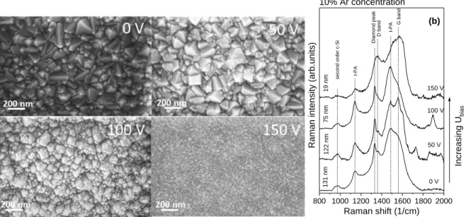
Modification of film morphology in NCD films, especially the diamond grain size could be achieved by systematic variation of the deposition parameters, like Ar-concentration of the feed gas and self- bias voltage (Ubias) of the substrate, while the other parameters are fixed. One series of NCD layers were prepared at 10% Ar-content with variation of the self-bias in the 0-150 V range. The influence of self-bias on the morphology of these films can be seen on SEM images (Figure 1a.). It can be seen that Ubias has a remarkable influence on the surface topography and the grain size of the formed films.
Diamond crystals with clearly distinguishable facets can be seen on the SEM images except for the film deposited at 150 V self-bias. The average grain size on the 0-50 V samples is around 100 nm. The first signs of the re-nucleation process are recognizable on the SEM image of the sample prepared at 100 V. The shape of bigger crystals is not well defined and smaller grains can be seen on their surface, which are the consequence of the re-nucleation caused by the increased growth speed. The film prepared at 150 V self-bias has uniform grain size distribution with 19 nm average size, characteristic for ultrananocrystalline diamonds.
800 1000 1200 1400 1600 1800 2000
t-PA
t-PA G band
D bandDiamond peak
Raman intensity (arb.units)
Raman shift (1/cm) 10% Ar concentration
131 nm122 nm75 nm19 nm Increasing Ubias
0 V 50 V 100 V 150 V
second order c-Si
(b)
Figure 1. SEM images (a) and Raman spectra (b) of nanocrystalline diamond layers of different grain sizes deposited at 0, 50, 100 and 150 V self-biases from feed gas with 10% Ar-content.
Raman scattering spectra of these samples are shown on Figure 1b. in the 800-2000 cm-1 wavenumber region. Every spectrum was normalized to its maximum and shifted along the ordinate for better visibility. The presented spectra are typical for nanocrystalline diamond films and they exhibit different scattering peaks assigned to different phases composing the film structure.
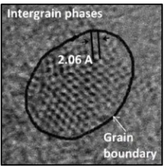
Nanodiamond films usually consist of diamond crystals, a non-diamond intergrain phase and the interface between these two, the so called grain boundary (Figure 2.). The characteristic Raman peak of bulk diamond crystals appears at 1332.3 cm-1 [13]. Raman spectra on Figure 1b. exhibit narrow peak at about 1333 cm-1 that can be assigned to diamond phase, however this band is hard to recognize on Raman spectrum of the 150 V sample. The peak position is shifted to higher wavenumbers (from 1332 to 1335 cm-1) with increasing self-bias due to the increasing residual stress in diamond
nanocrystals [14]. The well-known D and G bands near 1360 and 1560 cm-1, respectively, are related to the presence of intergrain phases. The G-peak is related to the stretching vibration of the sp2 C-C bonds (rings and chains), while the D-band is in connection with the breathing mode of the sp2 carbon containing rings. Nanodiamond fingerprint peaks (1140 and 1480 cm-1) usually appear in the Raman spectrum of nanosized diamond simultaneously and are related to the ν1 and ν3 modes of trans-
polyacetylene [15], respectively. The increasing intensity of the fingerprint peaks from 0 to 100 V refers to the higher amounts of grain boundary phases, but in case of the 150 V sample the intensive G-band is caused by the high intergrain sp2 carbon content. Additional relatively weak and broad band at 950-1000 cm-1 is related to the second-order Raman scattering of the crystalline Si substrate [16].
Figure 2. High-resolution transmission electron microscopy micrograph of a diamond nanocrystal.
Reprinted with permission from Reference 17.
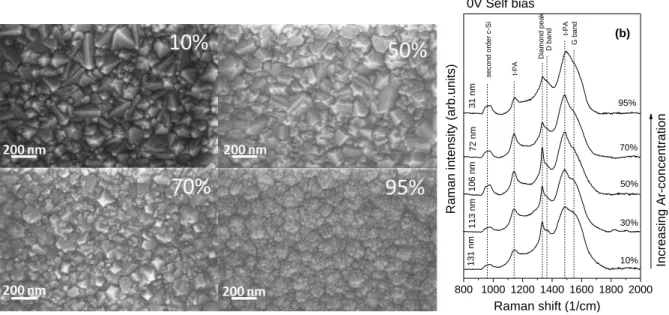
The influence of the Ar-content of the feed gas on the film morphology can be seen on SEM images (Figure 3a.) taken on layers deposited at 0 V self-bias with increasing Ar-concentration (10-95
%). Between 10-50% Ar-content the layers consist of definite crystals with average grain size decreasing with the Ar-ratio in the feed gas. Smaller crystals appear beside big ones in layers deposited at 70% Ar-content, while the highest Ar-concentration results in films consisting of small nanocrystrals only. Formation of UNCD layer with columnar growth takes place at these deposition parameters. The film surface is not uniform and the structure differs from the high self-bias samples, even though their average grain size is similar.
Raman spectra of samples grown at 0 V self-bias with increasing Ar-concentration are shown on Figure 3b. in the 800-2000 cm-1 wavenumber region. All spectra were normalized to their
maximum and shifted along the ordinate for better visibility. Characteristic Raman peak of diamond appears in the scattering spectrum of each sample, however its relative intensity decreases and the peak also broadens as the Ar-content of the feed gas increases. Diamond Raman peak can be found at 1334 cm-1 in the samples prepared at 10-70% Ar-concentration, while it is shifed to 1336 cm-1 in the case of 95% Ar ratio. The nanodiamond fingerprint peaks at 1140 and 1480 cm-1 characterize the bonding properties of grain boundarywhich change only slightly, as the peak positions do not vary with Ar-content. The changes of the G- and D-band parameters, however, indicate the modification of the bonding structure in the intergrain region. The estimation of the relative amount of diamond and non-diamond phases from the Raman spectrum produces unreliable results, because the scattering cross section is strongly dependent on the arrangement of the sp2 bonds.
800 1000 1200 1400 1600 1800 2000
G bandt-PA
D bandDiamond peak
t-PAsecond order c-Si
Raman intensity (arb.units)
Raman shift (1/cm) 0V Self bias
131 nm113 nm106 nm72 nm31 nm Increasing Ar-concentration
10%
30%
50%
70%
95%
(b)
Figure 3. SEM images (a) and Raman spectra (b) of nanocrystalline diamond layers with different grain sizes deposited at 0 V self-bias and 10, 30, 50, 70 and 95% Ar-content of the feed gas.
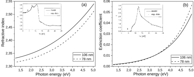
From the analysis of the SEM images and the Raman scattering results it can be concluded that the deposition parameters (self-bias and Ar-content of the feed gas) have significant influence on the structural properties and the morphology of the deposited NCD films. Further, the effect of the morphological changes on the optical properties should be explored. Optical properties of the deposited layers can be monitored by spectral ellipsometry, and by using this method we can determine the spectral dependence of the extinction coefficient and the refractive index in a wide photon energy range. Results obtained on two selected nanocrystalline diamond layers (grain size: 106 and 78 nm) are presented on Figure 4a. and 4b. in the 1.24-5 eV photon energy range. Refractive index (n) and extinction coefficient (k) curves measured and calculated on bulk diamond sample [18] are shown on insert of Figure 4a and 4b, respectively. The refractive index of diamond crystal changes between 2.4 and 2.7 in the 1.24-5 eV photon energy range, while the extinction coefficient is zero here [18]. In the case of nanocrystalline diamond layers the dispersion curve of refractive index is similar to that of diamond, but the values are between 2.32 and 2.54. This is due to the lower optical density of the NCD film. The influence of the non-diamond phases on the refractive index can be clearly seen on Figure 4a. The NCD layer with larger average grain size (106 nm) has a lower ratio of non-diamond phase (grain boundary and intergrain regions), thus its refractive index is closer to that of bulk diamond. According to the Figure, the increase of the non-diamond phase contribution results in a smaller refractive index of the NCD layer. It is well known that diamond is a transparent material from the UV (225 nm) to the far infrared, thus the extinction coefficient is zero below 5.5 eV photon energy, which is the band gap of bulk diamond (see Figure 4b insert). At the same time, due to absorption loss NCD layers have non-zero extinction coefficient values in the same photon energy range. The dependence of the extinction coefficient on the photon energy is very similar in the weak absorption region (up to ~3.5 eV) in the NCD layers of the two different (106 and 78 nm) grain sizes.
A more pronounced increase of the extinction coefficient can be observed from ~4 eV and the curve becomes steeper for the sample with smaller grain size (see Figure 4b.). This difference in the photon energy dependence indicates the increasing contribution of the non-diamond phases to the extinction coefficient. The absorption loss at photon energies below ~5.5 eV indicates the presence of localized states in the band gap of diamond. Non-diamond bonds, sp2 C=C, sp2 C=H, intrinsic and extrinsic
defects can contribute to the formation of these localized states. Raman scattering measurements confirm the presence of sp2 carbon phases in our NCD films and the change of their bonding structure and their spatial arrangement with the deposition parameters. Although the relative amount of these sp2 phases cannot be deduced from the Raman spectra. However it seems to be plausible that the ratio of sp2 phases increases with the decrease of the average grain size due to the higher surface area compared to the volume. Fluorescence measurements prove that NCD films exhibit relatively broad green (~2.3 eV) and blue (~3.2 eV) [19] luminescence bands attributed to intrinsic and in some cases extrinsic defects which also contributes to the localized states in the diamond band gap.
1,5 2,0 2,5 3,0 3,5 4,0 4,5 5,0 2,30
2,35 2,40 2,45 2,50 2,55
106 nm 78 nm
Refractive index
Photon energy (eV)
(a)
1,5 2,0 2,5 3,0 3,5 4,0 4,5 5,0 0,00
0,01 0,02 0,03 0,04 0,05 0,06
106 nm 78 nm
Extinction coefficient
Photon energy (eV)
(b)
Figure 4. (a) Spectral dependence of the refractive index (a) and the extinction coefficient (b) in nanocrystalline diamond films with average grain sizes of 106 and 78 nm. Spectral dependence of the
refractive index (Figure 4a insert) and the extinction coefficient (Figure 4b insert) of bulk diamond [18]. Triangles - experimental data; solid curve - model.
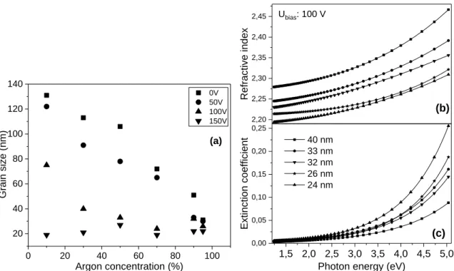
Next we will examine diamond films of average grain sizes below 40 nm. The average grain size as a function of deposition parameters for these films are depicted on Figure 5a. It can clearly be seen that self-bias voltage has significant influence on the average grain size at a given gas mixture composition. In general, UNCD films with less than 40 nm are formed above 50 V self-bias values.
With higher Ar-concentration even lower self-bias (0 and 50 V) is enough for the formation of films with grain sizes less than 40 nm (Figure 5a.). Series of NCD samples with average grain sizes close to those of so-called UNCD layers were chosen to represent changes in optical properties. Dispersion of the refractive index and extinction coefficient are plotted in Figure 5b. and 5c. for UNCD samples containing grains of 24-40 nm average size. Spectral dependence of the refractive index closely follows the characteristic behavior of the diamond crystal. However, in the case of 40 nm sample the values of the refractive index are around 90% of that of diamond crystals and with decreasing average grain size the refractive index shifts to smaller values. The increasing surface/volume ratio with smaller average grain size results in higher contribution of intergrain and grain boundary phases to the optical properties. The grain boundary and the intergrain phases contain different C-H bonds that cause lower average density of the UNCD layers, and thus the optical density also decreases.
0 20 40 60 80 100 20
40 60 80 100 120 140
0V 50V 100V 150V
Grain size (nm)
Argon concentration (%)
(a)
1,5 2,0 2,5 3,0 3,5 4,0 4,5 5,0
0,00 0,05 0,10 0,15 0,20 0,25
Extinction coefficient
Photon energy (eV)
(c)
2,20 2,25 2,30 2,35 2,40 2,45
40 nm 33 nm 32 nm 26 nm 24 nm
Refractive index
Ubias: 100 V
(b)
Figure 5. (a) Average grain size of analyzed NCD samples as a function of the deposition parameters.
Spectral dependence of the refractive index (b) and the extinction coefficient (c) in UNCD films with different grain sizes.
Photon energy dependence of extinction coefficient for UNCD samples is presented on Figure 5c. Significantly higher extinction coefficient values can be observed in UNCD films (<40 nm) compared to those of the NCD layers. The absorption loss is nearly 5 times larger in the UNCD sample with grain size of 24 nm. The extinction coefficient is inversely proportional to the average grain size in the analyzed photon energy range. The difference between the extinction coefficient curves for samples of different grain sizes increases rapidly above ~3 eV. The observed dependence of the extinction coefficient on the average grain size is closely related to the fact that the bonding structure and the spatial arrangement of non-diamond phases is influenced by the grain size. The large values of the extinction coefficient for UNCD samples indicate extra contribution to the absorption loss in these layers. Raman scattering spectra on Figure 1b. and Figure 3b. show a meaningful decrease of the diamond Raman peak relative to the scattering contribution of other phases, and this can be related partly to the smaller grain sizes. The relative scattering intensity of the G band increases for the sample with 19 nm grain size (Figure 1b.), although similar change cannot be observed for the 31 nm sample (Figure 3b.). The appearance of a new scattering band which can be assigned to the formation of a new type of structure, cannot be observed in these spectra, however it is possible that this structure does not have Raman active modes. Thus we suggest that the extra contribution to the extinction coefficient in UNCD films can be attributed to the significant increase in the amount of non-diamond phase caused by the higher surface/volume ratio. Beside the optical absorption, which is related to the non-diamond bonding structure, contribution of different defect sites, both intrinsic and extrinsic ones, has to be considered. For example, the increase of the extinction coefficient at ~4 eV could be related to the presence of substitutional N defects [20]. Luminescence excitation
spectroscopy performed on our UNCD samples confirmed these considerations.
4. Conclusions
Spectral dependence of the refractive index and the extinction coefficient were analyzed in nano- and ultrananocrystalline diamond layers. The average grain size was used as practical parameter for these layers, which is under 20 nm for the UNCD samples. The decrease of the average grain size indicates higher amount of non-diamond phases in the film structure. The evolution of the Raman scattering bands with the decreasing average grain size indicates changes in the bonding structure of the non- diamond phases. The difference between the optical parameters of nanodiamond layers and crystalline diamond in the whole studied spectral range becomes more pronounced as the average grain size of diamond layers decreases. This can be explained by the increasing ratio of non-diamond to diamond phases in the film. Since lower average grain size means larger grain boundary and intergrain region, the sp2 C-C and sp2 C-H bonds’ contribution to the localized states in the band gap of diamond increases, together with the average density of layers.
Acknowledgement
Sára Tóth is grateful for the support of the János Bolyai Research Scholarship of the Hungarian Academy of Sciences. This work was supported by the Hungarian Science Foundation under contract number NKFI K-115805. The authors also wish to thank P. Csíkvári for technical support.
References
[1] Kriele A, Williams O A, Wolfer M, Brink D, Müller-Sebert W and Nebel C E 2009 Appl. Phys.
Lett. 95 031905
[2] Kopecek M, Bacakova L, Vacik J, Fendrych F, Vorlicek V, Kratochvilova I, Lisa V, Van Hove E, Mer Ch, Bergonzo P and Nesladek M 2008 Phys. Status Solidi A 205 2146
[3] Auciello O, Gurman P, Guglielmotti M B, Olmedo D G, Berra A and Saravia M J 2014 MRS Bulletin 39 (Organic Spintronics) 621
[4] Williams O A and Nesladek M 2006 Phys. Status Solidi A 203 3375 [5] Gruen D M 1999 Annu. Rev. Mater. Sci. 29 211
[6] Hong B, Lee J, Collins R W, Kuang Y, Drawl W, Messier R, Tsong T T and Strausser Y E 1997 Diam. Relat. Mater. 6 55
[7] Silva F, Benedic F, Bruno P and Gicquel A 2005 Diam. Relat. Mater. 14 398 [8] Yugo S, Kanai T, Kimura T and Muto T 1991 Appl. Phys. Lett. 58 1036 [9] Auciello O and Sumant A V 2010 Diam. Relat. Mater. 19 699
[10] Herzinger C M, Johs B, McGahan W A, Woollam J A and Paulson W 1998 J. Appl. Phys. 83 3323
[11] Fujiwara H 2007 Spectroscopic Ellipsometry, Principles and Applications, John Wiley Sons Inc., New York
[12] Liu Y C, Hsieh J H and Tung S K 2006 Thin Solid Films 510 32
[13] Prawer S, Nugent K W, Jamieson D N, Orwa J O, Bursill L A and Peng J L 2000 Chem. Phys Lett. 332 93
[14] Bergman L and Nemanich R J 1995 J. Appl. Phys. 78 6709
[15] Brillante A, Hanfland M, Syassen K and Hocker J 1986 Physica B+C 139-140 533 [16] Mishra P, Jain K P 2001 Phys. Rev. B 64 073304
[17] Németh P, Garvie L A J and Buseck P R 2015 Scientific Reports 5 18381 [18] Aleksandra B. Djurisic and E. Herbert Li 1998 Appl. Optics 37 7273
[19] Himics L, Tóth S, Veres M, Czitrovszky A, Nagy A, Oszetzky D, Kerekes A, Kugler Sz, Rigó I, Tóth A, Koós M 2015 NATO Science For Peace and Security Series A: Chemistry And Biology 39 93 [20] Tucker O D, Newton M E and Baker J M 1994 Phys. Rev. B 50 15586