www.advmatinterfaces.de
Interparticle Interaction Matters: Charge Carrier Dynamics in Hybrid Semiconductor–Metal Cryoaerogels
Anja Schlosser, Jakob Schlenkrich, Dániel Zámbó,* Marina Rosebrock, Rebecca T. Graf, Giamper Escobar Cano, and Nadja C. Bigall*
DOI: 10.1002/admi.202200055
1. Introduction
Assembling nanoparticles (NPs) of dif- ferent material classes, namely, metals and semiconductors, into hybrid nanomate- rials not only merges the advantages of the counterparts but leads to even altered phys- icochemical properties pointing toward advanced applications.[1–3] While semicon- ductor NCs are able to produce charge car- riers upon photoexcitation, noble metals have a high electron affinity due to the position of their Fermi level within the energy landscape. The Fermi level posi- tion of the metal in the bandgap of the semiconductor allows the separation of the photoexcited electrons in the ps range,[4]
leading to electrons in the metal domains with long lifetimes up to tens of µs.[5,6] The efficiency of this charge carrier separation is governed by the nature of the interface between the components[7] as well as the recombination kinetics inside the semi- conductor heterostructures.[8,9] This effec- tive charge carrier separation has been discussed recently to be of high interest for, e.g., applications in photocatalysis.
When it comes to applications, nanoparticles frequently need to be assembled in a way that the physicochemical proper- ties are either conserved or even extended in a most beneficial way. In this regard, hydrogels and aerogels of nanoparticles are highly interesting, as they are self-supporting networks only consisting of the nanoscopic building blocks, and since they are at the same time highly voluminous, monolithic, and have enhanced surface accessibility to their hierarchical nanoporous architectures.[2,3,10–25] Nanocrystal hydrogels and aerogels can be prepared via chemical or physical methods.[1–3,26]
With respect to the design of multicomponent hydrogels and aerogels from noble metal and semiconductor compounds, there have solely been very few reports so far: Hendel et al.
reported on mixing of CdTe and noble metal nanoparticles resulting in arbitrary distribution of the gold domains in the network.[27] Similar applies for Rosebrock et al. who were able to form a CdS network with CdSe domains inside in combina- tion with an arbitrary distribution of the noble metal particles to control the spatial extent of fluorescence quenching.[28]
Zámbó et al. observed an in situ gelation and noble metal domain formation upon addition of multivalent metal ions to similar semiconductor nanocrystal building blocks resulting in Integration of noble metals into semiconductor-based nanoparticle gel
structures facilitates the extraction of photoexcited charge carriers upon illumination. While charge carrier generation takes place in the semicon- ductor component, noble metals in contact to the semiconductor act as electron sinks. Thus, the nature of the interface between the components is of essential importance, as it dictates the characteristics of the interparticle contact. Here, the influence of the nanoscale building block design on the charge carrier dynamics in cryoaerogels consisting of CdSe/CdS nanorods and nanoplatelets as well as of gold or platinum is reported. It is shown that direct growth of noble metal domains onto the semiconductor prior to the gelation significantly facilitates charge carrier separation in their cryoaerogel structures compared to gels from the colloidal mixtures of semiconductor and noble metal nanoparticles, the latter ones having less defined metal/
semiconductor boundaries and much more arbitrary component distribu- tions. Although the structure of the different cryoaerogel systems is similar at the micro- and macroscale, nanoscale differences caused by the two syn- thetic routes drive essentially different behavior regarding the charge carrier dynamics efficiency. These effects are observed spectroelectrochemically via intensity-modulated photocurrent spectroscopy emphasizing the importance of the semiconductor–metal connection in the hybrid structures.
A. Schlosser, J. Schlenkrich, D. Zámbó, M. Rosebrock, R. T. Graf, G. Escobar Cano, N. C. Bigall
Institute of Physical Chemistry and Electrochemistry Leibniz Universität Hannover
Callinstr. 3A, 30167Hanover, Germany
E-mail: daniel.zambo@pci.uni-hannover.de, daniel.zambo@ek-cer.hu;
nadja.bigall@pci.uni-hannover.de D. Zámbó
Centre for Energy Research
Institute of Technical Physics and Materials Science Konkoly-Thege M. str. 29-33, Budapest 1121, Hungary N. C. Bigall
Cluster of Excellence PhoenixD (Photonics, Optics and Engineering – Innovation Across Disciplines) Leibniz Universität Hannover
30167 Hanover, Germany
The ORCID identification number(s) for the author(s) of this article can be found under https://doi.org/10.1002/admi.202200055.
© 2022 The Authors. Advanced Materials Interfaces published by Wiley-VCH GmbH. This is an open access article under the terms of the Creative Commons Attribution-NonCommercial License, which permits use, distribution and reproduction in any medium, provided the original work is properly cited and is not used for commercial purposes.
a continuous semiconductor network with more homogeneous domain distribution.[11,29] Moreover, the use of hybrid nano- structures and alloys in photoelectrochemical applications has been shown for TiO2/Pt,[30] Zn1−xCdxSe/Pt,[31] and CdSe/CdS/Pt systems.[32]
However, when looking at the powerful tool of colloid chem- istry, establishing highly controlled metal/semiconductor con- tacts is also possible nowadays. This might open the possibility of a better control over both the distribution and the contact between the noble metal and the semiconductor in the aero- gels. Numerous elaborated wet-chemical synthesis methods of hybrid semiconductor/metal nanocrystals (NCs) have been demonstrated recently. The epitaxial deposition of metal domains onto semiconductor nanoplatelets (NPLs)[33–36] and nanorods (NRs)[7,37–41] by colloidal methods involving heteroge- neous nucleation facilitates the separation of the photoexcited electrons. Therefore, it essentially alters the optoelectronic properties compared to the pure semiconductor materials.
Upon illumination of CdSe/CdS dot-in-rods, electrons can delo- calize in the rod-shaped CdS shell, while the holes are being trapped in the CdSe core quantum dot.[42] This can occur, due to the small conduction band offset in the CdSe/CdS heterojunc- tion. Especially for core/crown NPLs, this intrinsic separation does not take place: the high exciton binding energy favors the recombination of the exciton in the CdSe core of the platelet.[9]
Nonetheless, applying bias potential on Cd-chalcogenide NPL networks can overcome the high exciton binding energy leading to effective charge carrier separation.[43]
We have demonstrated recently that charge carrier sepa- ration in hybrid semiconductor–metal nanoparticle gels can take place as well. In our work, photoexcited electrons were extracted and consumed in electrochemical processes in CdSe/CdS/Au hybrid gel networks prepared via the oxi- dative or ionic gelation of the hybrid nanoparticles.[44] By varying the number and location of the gold domains grown directly onto the semiconductor NR surface prior to gelation, the efficiency of the electron extraction from the semicon- ductor to the noble metal domain can be tuned. Mixing and co-gelating CdSe/CdS NRs and Au NPs via H2O2 led to the formation of hyperbranched solvogel and aerogel networks, where the extent of the photoluminescence quenching is highly dependent on the number and spatial distribution of the Au NPs within the gel network as well as the dielectric constant of the solvent in the gap between the nanorods and Au NPs.[28] These gel structures, however, were produced by means of partial oxidation and removal of the surface ligands, therefore, direct interparticle contacts were able to be achieved facilitating the formation of a branched semicon- ductor backbone.
As an important finding in the present work, a crucial dif- ference between gel structures consisting of hybrid CdSe/
CdS/Au NRs or CdSe/CdS/Pt NPLs (meaning that the metal domains are directly grown onto the semiconductor compo- nent), and co-gelated colloidal mixtures of the two components was found: the nature of the contact between the semicon- ductor and the metal domain/NP governs the charge carrier dynamics.
Beside the widely used chemical gelation methods, cryoge- lation is a novel physical gelation technique, which includes
the flash-freezing and the subsequent freeze drying of the aqueous NC solutions.[18] Its versatility and ease (no oxida- tive ligand removal is required in the process) allowed us to fabricate various, highly porous nanoparticle gel structures from noble metal NPs,[20,45–47] semiconductor NPLs,[43] metal oxide NPs[18] as well as mixed systems.[19] These structures proved their potential in applications such as electrocatalysis and electrochemical sensing. In the present work, we use this method for combining semiconductor and noble metal components within the cryoaerogels leading to hybrid nano- structures, which display the advantages of both components.
As we have a physical assembly method and not a chemical one, the surface chemistry of the assembled nanoparticles is of inferior importance and works regardless which route we choose: mixing semiconductor and noble metal nanoparticles or gelating semiconductor–metal hybrid nanoparticles. Thus, this method is beneficial for comparing different particle systems (in terms of the shape and ligands of the semicon- ductor and the type of the noble metal) without influencing the ligand coverage of the nanoparticles during the assembly.
However, as we have experienced so far, in case of citrate-stabi- lized metal nanoparticle-based cryogels, the large-scale attrac- tive forces during the freezing process are able to overcome the repulsive ligand-related interparticle forces, which leads to the welding of the metal nanoparticles.[45,46] To suppress this effect, thiolated surface attached molecules were used in the present work.
The following key questions inspired this work:
(i) Can a physically gelated hybrid gel network be effective in charge carrier separation?
(ii) Has the wet-chemical growth of the noble metal on the semiconductor an influence on the charge carrier separa- tion in comparison to mixed semiconductor and metal na- noparticles in cryoaerogel structures?
(iii) Is it possible to control the distribution of noble metal NPs in mixed co-gelated structures as precisely as for the gel net- works built up from originally hybrid semiconductor/metal nanoparticles?
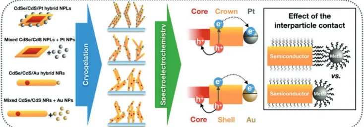
To answer these questions, we prepare hybrid cryoaerogel coatings on conductive ITO-coated glass substrates and inves- tigate these materials by means of structural and spectroelec- trochemical methods. The highly porous hybrid cryoaerogels consist of either CdSe/CdS core/crown nanoplatelets or dot- in-rods and additionally a noble metal component Pt and Au, respectively. The different metals for the NPL and NR systems are used due to synthetic limitations regarding the growth and phase transfer of gold on CdSe/CdS NPLs and Pt on CdSe/CdS NRs. Nevertheless, the different metals, thus, show the general validity of the results. Beside the preparation of pristine semi- conductor cryoaerogels, structures from semiconductor–metal nanoheteroparticles (in which the metal domains are directly grown onto the semiconductor NCs) as well as from mixed semiconductor and noble metal colloidal solutions are prepared (Scheme 1). We introduce here the following abbreviations to improve the readability: h-NPLs and h-NRs are used for the wet- chemically grown heterosystems (h), while m-NPLs and m-NRs refer to the mixed (m) gels. The used preparation methods represent two different approaches, which lead to essentially
different structures at the nanoscale. While the direct semi- conductor–noble metal contact is ensured in a defined way for the hybrid NCs, it is of rather undefined nature for gelating the colloidal mixtures of the two counterparts. In other words, the presence of ligands between the semiconductor and the metal can hinder the direct crystal contact in the cryoaerogel prepared from the colloidal mixture of the components. As we demon- strate, this structural difference at the nanoscale dramatically alters the charge carrier dynamics in the hybrid cryoaerogels:
direct growth of the noble metal domains facilitates an effective charge carrier separation upon illumination. However, the sep- aration of photoexcited electrons is significantly suppressed in the mixed systems. Intensity modulated photocurrent spectros- copy (IMPS) sheds light on the effect of the nanoscale design on the spectroelectrochemical response of the cryoaerogels.
Notable amounts of negative photocurrent can solely evolve in the case of directly grown noble metals, which show their superior performance in the charge carrier separation process.
Due to the versatility of the cryogelation method, these findings can further be adopted to other semiconductor–metal hybrid gel structures being active in photoelectrochemical sensing or photocatalysis.
2. Results and Discussion
2.1. Structure of Semiconductor–Metal Hybrid Cryoaerogel Electrodes
To reveal the effect of nanoscale design on the assembled structures, three nanorod-based and three nanoplatelet-based model systems were established. Pristine semiconductor NRs and NPLs, metal decorated h-NRs and h-NPLs (via direct dep- osition of metal domains) as well as mixed colloidal solutions of semiconductor and metal NPs were prepared according to our previous studies or based on synthetic procedures adapted from the literature (see the Experimental Section for details).
These building blocks (see Figures S1–S5, Supporting Infor- mation, for their characterization) were assembled into cry- oaerogels. To enable the electrochemical characterization of these gel networks, coatings on functionalized ITO elec- trodes were fabricated (photographs of the cryoaerogel elec- trodes can be seen in Figure S8, Supporting Information).
After their synthesis in organic media, the nanoparticles were transferred to the aqueous phase (via using MPA or MUA as ligand) and were distributed in a preformed mold on the sur- face of MPTMS-coated ITO glass followed by flash-freezing with cooled liquid isopentane (corresponding to a freezing temperature of 113 K).[43] This step was carried out by placing the electrode on the surface of the liquid isopentane until the liquid nanoparticle film was frozen. We have shown recently (for metal nanoparticles) that the freezing medium itself has a direct impact on the structure of the cryoaerogel coatings due to the various freezing velocity and ice crystal nucleation rate in different media.[46] Using liquid nitrogen, the domi- nating structures are lamellar sheets, however for isopentane, the high freezing velocity leads to cryoaerogel coatings with dendritic sheet structures with open porosity. The latter also showed enhanced stability in electrochemical processes,[45]
which is of great importance in the practical use of cryoaerogel coatings.[47]
The microstructure and elemental composition of the cry- oaerogels were investigated with scanning electron microscopy (SEM) and energy dispersive X-ray spectroscopy (EDXS).
Figure 1 shows the typical dendritic structures consisting of interconnected sheets for the pure NPLs and NRs, the h-NPLs and h-NRs as well as for the co-gelated mixtures of semicon- ductor and metal nanoparticles. These sheets have dimensions of tens of micrometers which is three magnitudes larger than the size of the nanoparticles building blocks itself. The highly porous nature of the coatings endows the systems with high accessible surface areas for interfacial reactions, which is a sig- nificant advantage over their simply drop-cast nanoparticle film counterparts.[43,46,47]
Scheme 1. Schematics of the investigated model systems: nanoparticle building blocks (NPLs and NRs) are combined with noble metals at the nanoscale (via direct growth of the metal domains or mixing the semiconductor and noble metal colloidal solutions). The hybrid or mixed nanoparticle solutions are cryogelated to fabricate aerogel-coated ITO electrodes. The charge carrier dynamics is studied via spectroelectrochemical tools to shed light on the impact of the nanoscale design (i.e., interparticle contact) on the charge carrier dynamics.
As the particle concentrations were uniform for all the inves- tigated systems, slight structural differences (e.g., distance of interconnected sheets, film thickness, sheet structure) can be attributed to the composition of the nanoparticle solutions, the differences in the shape of the NPs and the chain length of the NP ligands. The amount of free organic ligands in the solutions plays an important role in the structural properties of the coat- ings. Consequently, the nanoparticle solutions were purified to ensure the removal of excess ligands down to the limit of the colloidal stability. At the macro- and microscale, semicon- ductor–metal hybrid cryoaerogels show similar distribution of the metal nanoparticles (in the mixed systems) and the metal domains (for decorated NPs) in the elemental maps: the metals seem to be homogeneously distributed in all structures (see
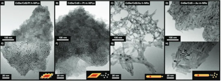
Figure S9 Supporting Information). Nonetheless, investigation on the nanoscopic structure of the cryoaerogel sheets sheds light on the difference regarding the distribution of the metal NPs and domains in the hybrid structures (Figure 2). Nano- platelets show different orientations on the transmission elec- tron microscopy (TEM) images (Figure 2A,B,E,F) leading to low contrast plates or wire-like structures with higher contrast.
This can be attributed to the 2D nature of the four-monolayer (ML) thick NPLs which can stand upright or lay on the grid.
While the growth of Pt directly on the NPLs leads to a homoge- neous distribution of the metal in the cryoaerogel, always a few Pt-NPs are in close vicinity in case of mixing and co-gelation of NPLs and Pt NPs (Figure 2B,F). This phenomenon can also be observed for the nanorod-based systems: Au nanoparticles
Figure 2. Nanostructure (lower and higher magnification TEM images) of cryoaerogel coatings consisting of A,E) h-NPLs, B,F) m-NPLs, C,G) h-NRs, and D,H) m-NRs.
Figure 1. Microstructure of cryoaerogel coatings consisting of A) pure NPLs, B) h-NPLs, C) m-NPLs, D) pure NRs, E) h-NRs, and F) m-NRs.
accumulate in distinct areas leading to an inhomogeneous gold distribution in case of mixing, however, cryogelation of h-NRs ensures the homogeneous distribution of gold. Based on our recent finding that the nature of interparticle connec- tion between CdSe/CdS NRs and Au NPs essentially governs the optical properties (extent of fluorescence quenching) of the hybrid gel structures,[28] the differences in the metal distribu- tions observed in these hybrid cryoaerogels are expected to have a significant impact on the spectroelectrochemical properties.
2.2. Optical Properties
The optical properties of the hybrid cryoaerogel electrodes show the characteristics of both the semiconductor and the metal components, respectively. From metal point of view, gold shows a distinct surface plasmon resonance (LSPR) in the visible wavelength range, while platinum has a broad, decay-like extinction (spectra of the nanoparticles can be seen in Figure S4, Supporting Information). This broad extinction of the Pt domains and NPs manifests itself in an increased absorption above 560 nm for the NPL-based hybrid cryoaero- gels (Figure 3A). The characteristic excitonic transitions of the CdSe/CdS NPLs remain visible in the spectra of hybrid cry- oaerogels, and the nanoscale design of the preparation (namely, the gelation of h- NPLs or the mixing and co-gelation of NPLs and Pt NPs) has solely slight impact on the overall absorption of the gel structures. This is a consequence of the size of the Pt domains and Pt NPs kept quasi-constant for both model sys- tems. Due to the metal growth on the nanoplatelets, a decrease in oscillator strength of the semiconductor can be observed.
As the LSPR of Au NPs is located at 519 nm, the metal con- tent leads to an increased absorption of the NR-based hybrid cryoaerogel coatings above 500 nm (Figure 3B) similar to the Pt for NPLs. Nevertheless, due to the similar size of the gold domains (grown on the NRs) and the Au NPs (in the mixed system), h-NR and m-NR cryoaerogels show comparable optical response. In case of the semiconductor–metal hybrid nanopar- ticles, the location of the LSPR is bathochromically shifted and becomes broader compared to the colloidally dispersed Au NP solution. This can be attributed to the refractive index change in the vicinity of the Au NPs[48] as well as to the possible Au NP-Au NP connections in the gel structures. The absorption of the CdSe core at 600 nm and the contribution of the LSPR of the Au domains and particles dominate the spectra of the gels.
The absorption of the CdS shell becomes prominent below 470 nm, which is in agreement with the band edge of the CdS and the characteristics of the typical CdSe/CdS gel structures due to the high particle concentrations.[10,11]
To shed light on the changes of the radiative lifetime of the excited carriers in all cryoaerogel systems, photoluminescence lifetime measurements were performed. Figure S6 (Supporting Information, for NPLs) and Figure S7 (Supporting Information, for NRs) show significant differences in the radiative lifetimes of the cryoaerogels prepared by means of different strategies.
Due to the high exciton binding energy, the pristine NPL cry- oaerogel shows a shorter lifetime than the one consisting of pristine NRs. In all systems, while growing the metal domains directly on the semiconductor leads to a drastic shortening of
the measured lifetimes, mixing exerts a lower influence on the recombination kinetics. This implies a more efficient charge carrier separation in the h-NPLs and h-NR cryoaerogels, which was further investigated via spectroelectrochemical methods.
2.3. Photoelectrochemical Investigations
Although the macrostructural properties of the different inves- tigated systems are similar, the semiconductor–noble metal interface as well as the distribution of the noble metal particles (i.e., the nanostructure of the co-cryogelated systems) essen- tially differ. As cryogelation is a physical method, the surface ligands play an important role in the nature of the connection between the building blocks. The aforementioned points are of central importance in terms of the charge carrier dynamics in the hybrid cryoaerogels.
To reveal these differences, spectroelectrochemical measure- ments have been performed. Linear sweep voltammetry (LSV) Figure 3. Optical properties of cryoaerogel coatings based on A) CdSe/
CdS NPLs and B) CdSe/CdS NRs.
was applied to shed light on the photocurrent directions and the photocurrent intensities as a function of the applied bias potential. Moreover, as a deeper insight into shorter time scales of the electrochemical response upon irradiation, intensity modulated photocurrent spectroscopy (IMPS) was used to gain resolutions up to the microsecond range. IMPS is a frequency dependent measurement technique where the photocurrent is monitored via sinusoidally modulated light pulses.[49] By varying the frequency of the light pulses, the evolution of the photocurrent from microseconds to seconds can be monitored.
A detailed description of the measurement is given in the (Sup- porting Information). In the following, different cryoaerogel systems will be compared and discussed: cryoaerogels prepared from the pristine semiconductor NPLs or NRs, from semicon- ductor/metal NPLs or NRs as well as from the mixed semicon- ductor and metal nanoparticles.
2.4. Nanoplatelet-Based Hybrid Cryoaerogels
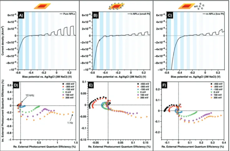
The results of the photoelectrochemical characterization of the NPL-Pt hybrid cryoaerogels are displayed in Figure 4. From the LSVs (Figure 4A–C), the total photocurrent amount and direc- tion in the equilibrium state dependent on the applied bias potential can be derived. Pristine CdSe/CdS NPLs (Figure 4A) show solely positive photocurrents which increase with
increasing bias potential. Hence, hole scavenging from the valence band is expectedly favored over electron transfer from the conduction band especially at high bias potentials.[43,50] In the low bias potential region, no net photocurrent is produced by the system, only a remarkable decrease of the dark current due to increased proton reduction is visible. These charac- teristics are related to the high exciton binding energy in the NPL system, which is a clear difference compared to the NRs (Section 2.5). For the Pt-decorated NPLs (Figure 4B) and the mixed system (Figure 4C), this feature becomes even more pro- nounced due to the presence of the noble metal particles. In addition, both platinum-containing systems are characterized by lower overall photocurrents compared to the pristine CdSe/
CdS NPL system. This effect might have been caused by a com- parably high light absorption of the Pt particles and/or electron back transfer processes from the metal to the semiconductor domain. However, the contribution of the latter processes is negligible due to the chosen irradiation wavelength and inten- sity. Remarkable amounts of negative net photocurrents are only generated by the cryoaerogel consisting of h-NPLs.
By means of IMPS, the time-dependent charge carrier dynamics was investigated more in depth. In case of the h-NPL system, a turnaround from negative to positive photocurrents can be noticed at low negative bias potentials (−150 to 0 mV).
Hence, processes leading to negative photocurrents, namely, proton reduction and electron transfer from the electrode,
Figure 4. A–C) LSVs and D–F) IMPS Nyquist plots of cryoaerogel coatings prepared from pure CdSe/CdS NPLs (A,D), h-NPLs (B,E), and m-NPLs (C,F). Blue shaded areas represent the regimes where the sample was illuminated.
are faster than the corresponding processes leading to posi- tive photocurrents. Upon further decreasing the bias poten- tial, the IMPS does not cross the imaginary axis but remains close to the equilibrium (real axis) at low frequencies. A similar behavior cannot be observed for pure CdSe/CdS NPLs. In this system, the net photocurrent at high bias potentials is orders of magnitudes higher than the net photocurrent at low bias potentials. The described differences in the photoelectrochem- ical properties of both systems can be attributed to the metal particles grown directly onto the surface of the nanoplatelets.
Due to the high electron affinity of Pt and the Fermi level of Pt being located within the bandgap of the CdS, efficient charge carrier separation takes place at the semiconductor–metal inter- face.[50] Hence, in h-NPLs, holes will accumulate in the semi- conductor domain, more specifically in the CdSe core, whereas electrons will preferably be located in the metal domain upon irradiation.[33] This leads to enhanced charge carrier lifetimes and a strongly increased availability of the excited electrons for electrochemical reactions. However, in pristine NPLs, the band alignment facilitates the recombination of both charge carriers in the CdSe core due to the high exciton binding energy, unless an external driving force (e.g., a bias potential) is applied. It must be noted, that the m-NPL system also shows negative photocurrents, though only at low bias potentials (lower than
−300 mV). Due to the high ionic strength of the electrolyte, electron transfer can take place between the semiconductor and the metal nanoparticles, however, the higher interparticle dis- tances decrease the efficiency of this transfer significantly.[28]
In a cryoaerogel, the single NPLs are in close proximity to each other forming stable sheets as can be seen in the TEM images (Figure 2A,B,E,F). This morphology allows the move- ment of charge carriers within the semiconductor backbone at certain bias potentials. In the IMPS, electron diffusion is reflected in the appearance of a second low-frequency semi- circle especially at high bias potentials.[11,12,43,51] For pristine NPLs, the high frequency semicircle has a larger diameter than the low frequency semicircle, implying that direct electron transfer at the electrode–particle interface contributes more effectively to the photocurrent than electron diffusion pro- cesses from electrode-far sites through the gel network to the electrode. A similar behavior can be observed for the m-NPL cryoaerogel, which indicates that Pt is likely not in direct con- tact with semiconductor platelets. This can be explained by the assumption that in this system both types of building blocks are separated by organic ligands and not in direct contact of the inorganic parts. Similar to other noble metals, Pt has a high sulfur affinity, hence MUA cannot be easily stripped from the surface. This assumption is further corroborated by the fact, that the m-NPL cryoaerogels are still strongly luminescent.
In contrast, the luminescence is fully quenched in case of on- grown h-NPLs or their cryoaerogels. The IMPS response of the on-grown system is characterized by an inverted ratio of both semicircles compared to the other systems. To reveal the influ- ence of the Pt load on the structural and spectroelectrochem- ical properties, cryoaerogels from hybrid NPLs with more Pt domains as well as from mixed solutions of NPLs and more Pt NPs were prepared (Figures S10 and S11, Supporting Informa- tion, show the structural properties). According to our expecta- tions, the inverted semicircle ratio is even more pronounced for
NPLs with more on-grown Pt domains (Figure S12, Supporting Information). Thus, it can be attributed to the direct contact between CdS and the Pt domains in the epitaxially grown systems.
In summary, the photoelectrochemical response of all NPL systems shows important differences governed by the nano- scopic design of the corresponding systems. Notable amounts of negative photocurrents are only produced by h-NPLs, that is, nanoplatelets with directly on-grown Pt particles. This behavior was related to the highly effective charge carrier separation at the semiconductor/metal interface. In addition, the IMPS response of this system at high bias potential, more precisely the ratio of the two semicircles, was inverted if compared to the pristine CdSe/CdS NPLs and the mixed system. This result means that efficient charge carrier separation in cryoaerogels can be achieved by direct synthesis of Pt particles on the semi- conductor surface and subsequent gelation but not by co-cryo- gelation of CdSe/CdS NPLs and Pt particles.
2.5. Nanorod-Based Hybrid Cryoaerogels
Model systems prepared from CdSe/CdS NRs and Au show similar spectroelectrochemical responses to the NPL-based cryoaerogels. Figure 5 shows the LSVs and the IMPS Nyquist plots of the nanorod-based samples. In the LSV measurements (Figure 5A–C), both hybrid cryoaerogels (h-NRs and m-NRs) as well as the pristine semiconductor cryoaerogels show a dominating positive photocurrent over the entire bias potential range, which is similar to the observations of Miethe et al. for semiconductor xerogels prepared by chemical destabilization.[51]
Major differences in the photocurrent evolution can be observed in the negative bias potential range. In case of the pure NRs and the mixed m-NRs, transients with higher posi- tive photocurrents can be observed at negative bias potentials directly after the beginning of the illumination. Importantly, these transients cannot be observed for the semiconductor–
metal hybrid nanoparticle cryoaerogel. Furthermore, this course of the photocurrent is of a significant difference com- pared to the NPL systems. Due to the high exciton binding energy emerging in the NPLs, the charge mobility is less effi- cient and thus no transients in the LSV measurements occur.
The high positive photocurrent and the following decrease to an equilibrium is correlated to an electron transfer toward the ITO electrode and a back electron transfer from the electrode to the nanoparticle gel network.[52] This indicates that the elec- tron transfer from the semiconductor to the ITO electrode over- weighs the electron transfer from the semiconductor into the solution in case of pristine nanorods. For mixed semiconductor and metal nanoparticles, the same behavior can be observed.
Meaning, the electron transfer from the semiconductor to the ITO electrode dominates over the transfer from the semicon- ductor to the metal particles and further the transfer into the solution. In the LSV of the semiconductor/metal hybrid nano- particle gels (h-NRs) no transients are visible which contrasts with the other two systems. Consequently, the transfer from the semiconductor to the metal domains and from the metal domain into the solution is competing with the transfer of elec- trons from the semiconductor to the ITO electrode (Figure S13,
Supporting Information). The competing processes lead to a reduced electron transfer to the ITO electrode resulting in diminished photocurrent transients at high positive photocur- rents. This firstly implies a significant difference between the mixed (m-NRs) and the grown semiconductor–metal hybrid cryoaerogels (h-NRs) regarding the charge carrier dynamics.
At more positive bias potentials, the LSV measurements of all three systems have the same course and no significant dif- ferences can be found. The back electron transfer is then less favored and the transfer of the electrons to the ITO electrode becomes more probable.[52] Additionally, the bias potential is close to the Fermi level of the semiconductor–metal systems which leads to a less favorable transfer of the electrons to the metal domain or metal particles.[53] Consequently, the semi- conductor component dominates the photocurrent response at positive bias potentials.
The IMPS measurements support the results of the LSVs and give further insight into the charge carrier dynamics. Dif- ferences in the IMPS spectra can also be observed mainly for negative bias potentials. The mixed semiconductor and metal nanoparticle cryoaerogel (m-NRs) shows similar spectra to the pure semiconductor nanorods. In this case, the measured photocurrent is positive for all measured bias potentials (from
−450 to 150 mV). As discussed at the LSV measurements, the electron transfer from the semiconductor to the ITO elec- trode is dominant which leads to the formation of semicircles
with a positive photocurrent. Since the maximum timescale of illumination is one second (equals to 1 Hz) for the IMPS measurements, the back electron transfer is likely to occur at even longer illumination durations. Nevertheless, the signs of trapped charge carrier recombination appear in the low- frequency regime, which become more prominent for the pure NR and mixed cryoaerogels (m-NRs). This manifests in the IMPS response in the first quadrant at very low frequen- cies, which is significantly suppressed for the h-NR structure indicating a mechanism with less loss in the charge carrier transport for the NRs with on-grown Au domains. Another characteristic which is known for connected semiconductor nanoparticle networks is that the IMPS spectra consist of more than one semicircle due to a photocurrent contribution of elec- trons which reach the electrode from particles locating further from the electrode.[43] This implies that the electrons can travel through larger fragments of the network by applying a potential gradient.[10,11,16] Consequently, even if in the cryoaerogel system the NRs are partially separated via organic ligands, positive bias potentials can represent enough driving force to tunnel the electrons one rod to another, similarly to the NPL networks discussed above. This becomes prominent at lower frequencies resulting in not two distinct semicircles but in an elongation of the semicircles toward higher positive photo currents. This elongation implies that the two semicircles overlap and mani- fest in a superposition of the two occurring processes: the direct Figure 5. A–C) LSVs and D–F) IMPS Nyquist plots of cryoaerogel coatings prepared from pure CdSe/CdS NRs (A,D), h-NRs (B,E), and m-NRs (C,F).
Blue shaded areas represent the regimes where the sample was illuminated.
electron transfer from the semiconductor particles to the ITO (for the first several layers of particles) and electron transfer throughout the network to the ITO.
In contrast, the cryoaerogel which consists of semicon- ductor/metal hybrid nanoparticles (Figure 5B) has different characteristics at negative bias potentials. For high frequencies, remarkable negative photocurrents evolve and reach a max- imum at a certain frequency followed by a turnaround toward positive currents. At low frequencies, all spectra end in the pos- itive photocurrent region that is consistent with the photocur- rents measured via LSV. The evolving negative photocurrents at high frequencies indicate that the electron transfer from the semiconductor to the metal domain and the transfer into the solution are dominating. The mechanism for the photocurrent evolution in semiconductor/metal hybrid nanoparticles is dis- cussed more detailed in our recent study.[44]
The results indicate that the NR-based and the NPL-based systems behave similarly and the nature of the interparticle connection between the semiconductor and metal components governs the charge carrier dynamics. Differences between the NR and NPL systems are attributed to the large exciton binding energy in the NPLs which leads to a lower charge carrier mobility. Pure semiconductor (NR and NPLs) cryoaerogels only provide positive photocurrent whilst the use of semiconductor–
metal hybrid nanoparticles enables a charge carrier separation within the different materials and the transfer of the electron into the solution, where it can be consumed by redox reac- tions. Mixing semiconductor and metal nanoparticles results in a decrease of the photocurrent and solely a low negative photocurrent in case of the NPL system. From photoelectro- chemical point of view, properties of m-NR cryoaerogels differ significantly from the cryoaerogels of h-NRs. Importantly, these differences between the mixed and on-grown systems under- line the importance of the semiconductor–metal crystal contact.
While there is a direct contact between the two components for the h-NR and h-NPL networks (originating from the epitaxial contact of the metal to the semiconductor), the indirect contact dramatically affects the properties in mixed and co-gelated sys- tems. This is likely a consequence of the presence of covalently bound ligands on both building blocks hindering the efficient electron transfer from the semiconductor toward the metal par- ticles.[28] Thus, the physical forces during the cryogelation do not overcome the repulsive forces of the ligands in contrast to the citrate-stabilized metal nanoparticle-based cryogels.[45,46]
Therefore, heterogeneous nucleation of the metal directly on the semiconductor and the resulting large crystal contact endows the cryoaerogels with advantageous properties in terms of charge carrier separation, which makes them a promising candidate for photoelectrochemical sensing purposes.
3. Conclusion
In summary, this work shows that the physicochemical proper- ties are strongly dependent on the nanoscopic and microscopic structural architecture in multicomponent aerogels consisting of semiconductor and noble metal nanoparticles. The nanoscale design of the building blocks has a great influence on the spectro- electrochemical properties in hybrid cryoaerogel structures. Pure
semiconductor, hybrid semiconductor/noble metal and mixed semiconductor–noble metal NCs were cryogelated into porous aerogels on conductive substrates to shed light on the efficiency of the charge carrier separation upon different approaches.
While the cryoaerogel structures show similar macrostructural properties, the distribution of the noble metal and the semicon- ductor–metal interface are of essential difference at the nano- and microscale. Homogeneous distribution of noble metal domains can be ensured for cryoaerogels of NRs and NPLs with on-grown metal domains. However, the mixing and co-gelation led to an uncontrollable distribution of the network components.
Additionally, the direct contact of the metal to the semicon- ductor compartments can be formed in case of on-grown metal domains (h-NRs and h-NPLs). Structural differences alter the charge carrier dynamics significantly: while charge carrier delo- calization in the semiconductor backbone governs the spectroe- lectrochemical response in pure and mixed systems (m-NRs and m-NPLs), charge carriers can effectively be separated in cryoaero- gels from semiconductor building blocks with on-grown noble metal domains. This underlines the limitation of simple mixing and co-cryogelation in terms of charge carrier separation due to the arbitrary distribution and presence of ligands hindering the effective electron accumulation in the metal domains upon pho- toexciting the semiconductor counterparts. These results further imply that the physical forces appearing during the cryogelation cannot overcome the ligand shell repulsion in the mixed sys- tems. Therefore, in mixed cryoaerogels (m-NRs and m-NPLs), tailoring the nanoscopic and microscopic structure regarding the component distribution, contact points of the components as well as the organic ligand shell possibly residing between the nanoparticles, is of essential importance. These findings point toward the utilization of hybrid cryoaerogel coatings in photoca- talysis and spectroelectrochemical sensing.
4. Experimental Section
Chemicals: Sodium myristate (≥99%), methanol (MeOH, ≥99.8%), cadmium acetate (99.995%), 1-octadecene (ODE, 90%), ethanol (EtOH, ≥99.8%), sulfur (S, ≥99.98%), isopropanol (iPrOH, ≥99.8%), 11-mercaptoundecanoic acid (MUA, 95%), iron(0) pentacarbonyl (Fe(CO)5, 99.99%), tri-n-octylphosphine oxide (TOPO, 99%), 1,2,3,4-tetrahydronaphthalene (tetraline, 99%), oleylamine (OAm, 70%), 3-mercaptopropionic acid (MPA, 99%), didodecyldimethylammonium bromid (DDAB, 98%), dodecylamine (DDA, 98%), and toluene (≥99.7%) were purchased from Sigma Aldrich. Tri-n-octylphosphine (TOP, 97%), platinum(II) acetylacetonate (Pt(acac)2, 98%), gold(III) chloride (AuCl3, 99%), and cadmium acetate dihydrate (98%) were obtained from ABCR.
Oleic acid (OlAc, 90%), cadmium nitrate tetrahydrate (99.999%), selenium (Se, 200 mesh, 99.999%), cadmium oxide (CdO), hydrogen tetrachloroaurate(III) trihydrate (HAuCl4·3H2O, 99.99%), and borane tert-butylamine complex (TBAB, 97%) were supplied by Alfa Aesar.
n-hexane (≥99%) was purchased from Merck. Oleylamine (OlAm, 80%–90%) was supplied by Acros. Hexylphosphonic acid (HPA, 99%) and octadecylphosphonic acid (ODPA, 99%) were purchased from PCI Synthesis. All chemicals were used as received without further purification. ODE applied for the preparation of TOP:S was degassed in vacuum at 100 °C for at least 6 h and stored in an air-free glovebox.
Synthesis of Cadmium Myristate: Cadmium myristate was synthesized following a literature procedure[9] without modifications.
Synthesis of CdSe Core Nanoplatelets (NPLs): Quasi-rectangular CdSe NPLs with a thickness of four MLs were synthesized according to literature procedures[43,54] with slight modifications. Briefly, 1360 mg
(2.40 mmol) of cadmium myristate and 96 mg (1.22 mmol) of Se were dispersed in 120 mL of ODE in a 250 mL three-neck flask. The reaction solution was degassed in vacuum twice for 30 min at 70 °C and was afterward heated to 240 °C under an Ar atmosphere. At 205 °C, a mixture consisting of 160 mg (0.60 mmol) of solid cadmium acetate dihydrate and 138 mg (0.60 mmol) of solid cadmium acetate was added swiftly to the reaction solution. After 9.5 min at 240 °C, 4 mL of OlAc was injected and the reaction was continued for further 30 s. The heating mantle was removed and further 4 mL of OlAc were added at ≈160 °C.
The reaction solution was purified by adding 40 mL of EtOH followed by centrifugation (4226 rcf, 10 min). The precipitates were redispersed in 60 mL of n-hexane and centrifuged again (4226 rcf, 10 min) to remove 3 ML NPLs. To the supernatant, 30 mL of ethanol was added. The four ML NPLs were collected by centrifugation (4226 rcf, 10 min) and were redispersed in 6 mL of n-hexane.
Synthesis of CdSe/CdS Core/Crown NPLs: To synthesize CdSe/CdS core/crown NPLs, a slightly modified literature procedure[55] was applied. In a 100 mL three-neck flask, 288 mg (1.08 mmol) of cadmium acetate dihydrate, 540 µL (1.70 mmol) of OlAc, and 2660 µL [calculated OD at first excitonic maximum (507 nm): 120.00] of the CdSe NPLs in n-hexane were dispersed in 24 mL of ODE. Subsequently, the solution was degassed in vacuum for 45 min at 60 °C. Under an Ar atmosphere, the dispersion was heated to 240 °C. Starting at 215 °C, a solution of 1100 µL 1 m TOP:S (prepared by dissolving elemental sulfur in TOP under stirring overnight in a glovebox) in 7.9 mL of ODE was injected with a syringe pump at a constant rate of 18 mL h−1. After completion of the injection, the solution was kept at 240 °C for another 40 min and afterward allowed to cool down to room temperature. The product was collected by addition of 10 mL of n-hexane and 20 mL of ethanol followed by centrifugation (4226 rcf, 10 min). The NPLs were redispersed in n-hexane (5 mL).
Platinum Growth on CdSe/CdS Nanoplatelets: For the platinum growth, a procedure by Naskar et al.[56] with slight modifications was applied. At first, 89.7 mg (0.23 mmol) of Pt(acac)2, 1 mL (3.03 mmol) of OlAm, 354 µL (Cd ion concentration: 131.18 mmol L−1) of the CdSe/
CdS NPLs in n-hexane, and 30 mL of ODE were combined in a 100 mL three-neck flask. The n-hexane was removed carefully in vacuum at room temperature and the dispersion was heated to 130 °C under an Ar atmosphere. Depending on the desired Pt size the solution was kept at this reaction temperature for 30 min (smaller domains, shown in the main text) and 60 min (larger domains, shown in the Supporting Information), respectively. To collect the Pt decorated NPLs, 45 mL of iPrOH and 60 mL of EtOH were added and the solution was centrifuged (4226 rcf, 10 min). Finally, the solids were redispersed in n-hexane (3 mL).
Synthesis of Spherical Pt NPs: Pt NPs were synthesized according to Naskar et al.[14] with slight modifications. Briefly, 200 mg (0.51 mmol) Pt(acac)2 and 1 mL (3.03 mmol) of OlAm were dispersed in 15 mL of ODE and degassed in vacuum at 40 °C for 45 min. Under an Ar atmosphere, the temperature was raised to 120 °C within 30 min. At this temperature, 120 µL of a previously prepared 1:10 (v:v) mixture of Fe(CO)5:ODE was injected with a syringe. The reaction temperature was then increased by 5 °C min−1 to 180 °C and the heating mantle was removed. At room temperature, 20 mL of iPrOH and 30 mL of EtOH were added and the solution was centrifuged (8000 rcf, 10 min). The Pt NPs were redispersed in 3 mL of n-hexane.
Phase Transfer of CdSe/CdS NPLs, CdSe/CdS/Pt h-NPLs, and Spherical Pt NPs: CdSe/CdS NPLs, CdSe/CdS/Pt h-NPLs, and Pt NPs were transferred to aqueous medium following a slightly modified literature protocol.[57] For the phase transfer of CdSe/CdS NPLs, 500 µL of the organic NPL solution was mixed with 2.5 mL of n-hexane and 4.24 mL of the phase transfer solution. CdSe/CdS/Pt NPLs were transferred by adding 3 mL of n-hexane and 5.63 mL of the phase transfer solution to 2.25 mL of the NPL solution. In both cases, the phase transfer solution consists of 280 mg (1.28 mmol) of MUA and 165 mg (2.94 mmol) of KOH dissolved in 20 mL of MeOH. For the phase transfer of spherical Pt NPs, 0.5 mL of the NP solution and 5.5 mL of n-hexane were mixed with 4 mL of the phase transfer solution. In this case, the phase transfer
solution consists of 30 mg (0.14 mmol) of MUA, 50 mg (0.89 mmol) of KOH, and 4 mL of MeOH. After mixing the solutions, the nanoparticles were shaken overnight to ensure complete transfer to the aqueous medium.
Afterwards, the vials were left undisturbed to separate the phases. The organic phase was removed and the methanolic phase was centrifuged (4226 rcf, 10 min). The solids were dispersed in 15 mL of 0.01 m KOH each and washed with 60 mL of 0.01 m KOH by means of a centrifuge filter. The centrifugation time of the last step was adjusted so that final solution volumes between 250 µL (CdSe/CdS/Pt NPLs and Pt NPs) and 500 µL (CdSe/CdS NPLs) were reached.
Synthesis of CdSe Core Nanoparticles (Seeds): The CdSe seeds were synthesized according to Carbone et al.[58] Typically, CdO (60 mg), ODPA (280 mg) and TOPO (3.0 g) were mixed in a 25 mL flask and were degassed in vacuum at 150 °C for 1 h. At 300 °C in an Ar atmosphere, the solution was stirred until CdO is dissolved to obtain a clear solution.
At this point, TOP (1.8 mL) was added, and the mixture was heated to 380 °C. A solution of selenium (58 mg) in TOP (1.8 mL) was swiftly injected and the reaction was quenched after 4 min by the addition of 4 mL ODE. The heating mantle was removed, and the seed solution was allowed to cool down to 90 °C, where 5 mL of toluene was added (to prevent the solidification of TOPO). The as-synthesized particles were purified by alternating addition of methanol (precipitation), centrifugation (8000 rcf, 10 min) and redispersion in toluene. The particles were finally stored in hexane and kept for CdSe/CdS shell growth.
Synthesis of CdSe/CdS Core/Shell NRs: The as-synthesized CdSe seeds were coated with an elongated CdS shell using the procedure of Carbone et al.[58] with slight modifications. First, CdO (60 mg), HPA (80 mg), ODPA (280 mg), and TOPO (9.0 g) were degassed under vacuum at 150 °C for 1 h. The solution was heated to 300 °C in an Ar atmosphere until CdO was completely dissolved. After the addition of TOP (1.8 mL), the solution was heated to 350 °C. At this point, the mixture of CdSe seeds (0.08 µmol), sulfur (130 mg), and TOP (1.8 mL) was quickly injected, and the reaction was stirred for 8 min before cooling down to room temperature. During the cooling, 5 mL of toluene was added at 90 °C. The CdSe/CdS NRs were purified by precipitation with methanol, centrifugation (3773 rcf, 10 min) and redispersion in toluene. This step is repeated three times before the CdSe/CdS NRs were finally stored in toluene (12 mL).
Gold Growth on CdSe/CdS NRs: According to the method published by Menagen et al.,[38] AuCl3 (10 mg), DDA (161.76 mg), and DDAB (101.2 mg) were mixed with toluene (24.12 mL) in a glovebox. The mixture was ultrasonicated for 15 min. When the solution became light yellow, it was mixed with the CdSe/CdS NR solution in toluene (27.2 mL, cCd = 0.156 mg mL−1) inside a glove box. The mixture was irradiated with an LED (Ledxon Alustar 9008098, λ = 470 nm, operated at 350 mA) for 45 min under stirring. Afterward, methanol (20 mL) was added to quench the reaction, and the solution was centrifuged. Furthermore, the particles were washed twice with methanol and redispersed finally in toluene (2 mL).
Synthesis of Spherical Au NPs: Spherical Au NPs were synthesized according to Peng et al.[59] in organic medium. HAuCl4·3H2O (100 mg) was dissolved in a mixture of tetraline (10 mL) and OAm (10 mL) at room temperature and ambient conditions by 10 min of stirring. TBAB (34.5 mg), tetraline (1 mL), and OAm (1 mL) were sonicated to dissolve the TBAB. The TBAB solution was quickly injected into the Au containing solution and stirred for 2 h at room temperature. For the purification of the particles, the solution was divided into multiple parts and separately precipitated with ethanol (35 mL per 11 mL synthesis solution) in 50 mL Falcon tubes. After centrifugation (8500 rcf, 10 min), the Au NPs were redissolved in toluene (5 mL).
Phase Transfer of CdSe/CdS NRs: The phase transfer was carried out by ligand exchange from TOP/TOPO to MPA according to Kodanek et al.[57] Colloidal CdSe/CdS solution in toluene (12 mL) was precipitated with methanol (12 mL) and redispersed in hexane (12 mL). A mixture of methanol (100 mL), MPA (2.6 mL), and KOH (1.14 g) was prepared and added to the 12 mL of NRs in hexane followed by shaking for 2 h at room
temperature. After phase separation, the NRs were centrifuged (10 min, 8500 rcf), redispersed in 0.01 m KOH (5 mL) solution and treated with 2 mL of chloroform to remove the excess of organics. After vortexing, the mixture was centrifuged (10 min, 8500 rcf) and the colloidal NR solution was carefully collected from the upper phase. Finally, the aqueous phase of CdSe/CdS was five times washed with centrifugation filters (30 k MWCO) and 0.01 m KOH (7 mL). The final concentration of NRs was determined by atomic absorption spectroscopy (AAS) measurements and set to ≈80 × 10−6 m.
Phase Transfer of Spherical Au NPs: The phase transfer of spherical Au NPs according to Hiramatsu et al.[60] was carried out by addition of MPA (4.5 mL) to a boiling solution of Au NPs in toluene (44 mg NPs in 90 mL toluene). The NPs were immediately precipitated as a black solid.
After centrifugation (10 min, 8500 rcf) the particles were redispersed in 0.01 m KOH (1 mL) and purified by centrifugation filters (30 k MCWO) as for CdSe/CdS. Finally, Au NPs concentration was determined by AAS measurements and set to ≈80 × 10−6 m.
Phase Transfer of Gold Tipped CdSe/CdS/Au h-NRs: The method of the phase transfer was adapted from the work of Kodanek et al.[57] The gold decorated particles were precipitated with methanol, centrifuged and redispersed in hexane (10 mL). The cadmium concentration was ≈0.4 mg mL−1. After the addition of methanol (10 mL) and MPA (0.125 mL) the mixture was shaken for 1 h. The methanolic phase including the particles was separated and centrifuged. After redispersion of the nanorods in 0.01 m aqueous KOH solution (2 mL), the particles were washed five times with acetone and finally redispersed in 0.01 m aqueous KOH solution (300 µL).
Preparation of Cryoaerogel-Coated ITO Electrodes: Before coating the electrodes with the particles, the ITO-coated glass substrates (VisionTek Ltd., 12 Ω square−1, size of 1.5 cm × 3 cm) were cleaned and activated.
For cleaning, the substrates were subsequently sonicated for 5 min in acetone, 2-propanol, and Millipore water. Afterward, the surface was activated with a solution of NH4OH and H2O2 (10 mL 25% NH4OH, 10 mL 35% H2O2) in water (50 mL) for 2 h at 70 °C under stirring. Next, the ITO surface was functionalized with 1 vol% MPTMS in toluene for 2 h at 70 °C under stirring. A mold (0.75 cm × 0.75 cm for all nanorod samples and 1.0 cm × 1.0 cm for nanoplatelet samples, respectively) was fabricated from adhesive tape and 20 µL cm−2 of the nanoparticle solution (c(Cd2+) = 70 × 10−3 m, in case of mixed systems with the addition of 2 µL Au NP c(Au3+) = 31 × 10−3 m) were distributed inside the rectangular mold (see more details in Table S1, Supporting Information).
To flash-freeze the aqueous nanoparticle solutions, the electrodes were placed on the surface of liquid 2-methylbutane (temperature: −160 °C) until the solution was frozen. Afterward, the electrodes were stored in liquid nitrogen overnight before drying the electrodes in the freeze dryer or in a freezer (at −20 °C), respectively.[43,45–47]
Photoelectrochemical Measurements: Photoelectrochemical measurements were carried out in a lab-designed Teflon cell, in which the prepared cryoaerogel coatings were carefully rehydrated by the supporting electrolyte (discussed below). For intensity modulated photocurrent spectroscopy, the current response of the electrochemical cell was measured while irradiating the cryoaerogel sample with an LED light source operating at frequencies between 10 kHz and 1 Hz. Hereby, the value of the generated photocurrent and the phase shift between the sinusoidal light pulses and the sinusoidal current signal is measured.
For this detection, a lock-in amplifier controls the sinusoidal light pulses with the specific frequency and links the outgoing signal to the incoming photocurrent detected by the potentiostat. A lock-in amplifier is necessary because a potentiostat in general is not able to adequately register the low and rapidly changing currents in the nA range, where the noise of the system is larger than the signal itself. These measurements were applied at different bias potentials between −450 and 150 mV (−450,
−300, −150, 0, 150, 300 mV). All given bias potentials are related to the applied Ag/AgCl reference electrode (3 m NaCl, purchased from BASi).
As electrolyte, a 0.5 m solution of sodium sulfite in Millipore water was applied throughout all measurements. The pH of the electrolyte solution was adjusted to 7 by addition of sulfuric acid prior to use. A PE 1542 DC power supply from PHILIPS powers the LED (0.5 mW, λ = 472 nm)
and a Signal Recovery 7270 DSP lock-in amplifier from AMETEK gives the sinusoidal signal to the LED as well as detects the current signal from the measurement cell. A Solatron Modulab XM potentiostat from AMETEK was used to apply the bias potential and to measure the generated photocurrents.
Measuring the linear sweep voltammetry includes a scan of a predefined bias potential range over a fixed time range. In the experiments, the voltage was applied from −0.6 V up to 0.3 V with a slope of 4 mV s−1. Before starting the measurement, a constant potential was applied for 30 s at the starting voltage of −0.6 V to reach the equilibrium state of the system. During the linear sweep voltammetry, the LED was turned on and off periodically with a frequency of 40 mHz.
This corresponds to a time period of 12.5 s of irradiation and 12.5 s of darkness. To apply the voltage and to register the current, a potentiostat (Solatron Modulab XM from AMETEK) was used. The LED was controlled by an arbitrary generator HMF2550 from Rohde & Schwarz.
Optical Spectroscopy: For the optical characterization, the nanoparticle solutions were diluted with the respective solvent and measured in quartz cuvettes with a volume of 1 or 3 mL (optical path length of 1 cm).
UV–vis extinction spectra of the samples were recorded by means of a Horiba Dual-FL, a Jasco V750, or an Agilent Cary 5000 UV–vis–NIR spectrophotometer. Emission measurements (PL emission spectra and photoluminescence quantum yields, PLQYs) were carried out on a Horiba Dual-FL (equipped with a Quanta-Phi integrating sphere for PLQY), a Horiba Fluoromax-4 or an Edinburgh Instruments FLS 1000 spectrofluorometer.
UV–vis absorption spectra of the cryoaerogel coatings were measured by means of an Agilent Cary 5000 UV–vis–NIR spectrometer equipped with DRA-2500 integrating sphere. The measurements were carried out in center-mount position and the sample holder was tilted by 10°
to ensure nearly perpendicular irradiation of the coating and to prevent direct back reflection to the optical illumination path.
Transmission Electron Microscopy: For TEM imaging, a FEI G2 F20 TMP equipped with a field emission gun operating at 200 kV was applied.
Images were either taken by means of a bright-field detector or a high- angle annular dark field (HAADF) detector in scanning TEM (STEM) mode. Diluted nanoparticle solutions were drop-cast onto carbon coated copper grids (Quantifoil, 300 mesh). In case of the cryoaerogels, the grid was gently pressed onto the cryoaerogel coating to transfer gel fragments onto the grid.
Scanning Electron Microscopy: Scanning electron microscopy (SEM) images were taken using a JEOL JSM-6700F scanning electron microscope (operated at 2 kV). SEM samples were obtained by immobilizing the cryoaerogel-coated ITO glasses on brass SEM holders using conductive paint (ACHESON 1415) to ensure the electrical contact between the ITO and the holder. SEM-EDX spectra were recorded in the energy range of 0–10 keV using an Oxford Instruments INCA 300 detector.
Atomic Absorption Spectroscopy: Cd and Au concentrations of the nanoparticle solutions were determined by AAS. Therefore, a certain amount of the solution was dried and mixed with 1 mL of aqua regia and left overnight for full metal dissolution. Afterward, the solution was diluted to 50 mL with MilliQ water. For all measurements, a Varian AA140 spectrometer equipped with hollow cathode lamps suitable to the different element absorption wavelengths was applied. The concentration of Pt was determined by SEM-EDX analysis.
Supporting Information
Supporting Information is available from the Wiley Online Library or from the author.
Acknowledgements
A.S. and J.S. contributed equally to this work. The authors would like to acknowledge the financial support from the European Research Council
(ERC) under the European Union’s Horizon 2020 research and innovation program (Grant Agreement No. 714429). In addition, this work was funded by the German Research Foundation (Deutsche Forschungsgemeinschaft, DFG) under Germany’s excellence strategy within the cluster of excellence PhoenixD (EXC 2122, project ID 390833453) and the grant BI 1708/4-1.
D.Z. acknowledges the program financed by the National Research, Development and Innovation Office of the Ministry for Innovation and Technology, Hungary (TKP2021-NKTA-05). A.S. and R.T.G. are thankful for financial support from the Hannover School for Nanotechnology (hsn).
The authors also thank Armin Feldhoff and Jürgen Caro for providing the SEM facility, and the LNQE for providing the TEM.
Open access funding enabled and organized by Projekt DEAL.
Conflict of Interest
The authors declare no conflict of interest.
Data Availability Statement
Research data are not shared.
Keywords
charge carrier separation, cryoaerogels, hybrid nanocrystal gels, semiconductor–metal hybrid gels, spectroelectrochemistry
Received: January 10, 2022 Published online:
[1] P. Rusch, D. Zámbó, N. C. Bigall, Acc. Chem. Res. 2020, 53, 2414.
[2] B. Cai, V. Sayevich, N. Gaponik, A. Eychmüller, Adv. Mater. 2018, 30, 1707518.
[3] C. Ziegler, A. Wolf, W. Liu, A.-K. Herrmann, N. Gaponik, A. Eychmüller, Angew. Chem., Int. Ed. 2017, 56, 13200.
[4] D. Mongin, E. Shaviv, P. Maioli, A. Crut, U. Banin, N. Del Fatti, F. Vallée, ACS Nano 2012, 6, 7034.
[5] E. Khon, A. Mereshchenko, A. N. Tarnovsky, K. Acharya, A. Klinkova, N. N. Hewa-Kasakarage, I. Nemitz, M. Zamkov, Nano Lett. 2011, 11, 1792.
[6] M. Wächtler, P. Kalisman, L. Amirav, J. Phys. Chem. C 2016, 120, 24491.
[7] Y. Nakibli, Y. Mazal, Y. Dubi, M. Wächtler, L. Amirav, Nano Lett.
2018, 18, 357.
[8] F. T. Rabouw, P. Lunnemann, R. J. A. van Dijk-Moes, M. Frimmer, F. Pietra, A. F. Koenderink, D. Vanmaekelbergh, Nano Lett. 2013, 13, 4884.
[9] M. D. Tessier, P. Spinicelli, D. Dupont, G. Patriarche, S. Ithurria, B. Dubertret, Nano Lett. 2014, 14, 207.
[10] S. Sanchez-Paradinas, D. Dorfs, S. Friebe, A. Freytag, A. Wolf, N. C. Bigall, Adv. Mater. 2015, 27, 6152.
[11] D. Zámbó, A. Schlosser, P. Rusch, F. Lübkemann, J. Koch, H. Pfnür, N. C. Bigall, Small 2020, 1906934.
[12] F. Lübkemann, J. F. Miethe, F. Steinbach, P. Rusch, A. Schlosser, D. Zámbó, T. Heinemeyer, D. Natke, D. Zok, D. Dorfs, N. C. Bigall, Small 2019, 15, 1902186.
[13] F. Lübkemann, P. Rusch, S. Getschmann, B. Schremmer, M. Schäfer, M. Schulz, B. Hoppe, P. Behrens, N. C. Bigall, D. Dorfs, Nanoscale 2020, 12, 5038.
[14] S. Naskar, A. Freytag, J. Deutsch, N. Wendt, P. Behrens, A. Köckritz, N. C. Bigall, Chem. Mater. 2017, 29, 9208.
[15] S. Naskar, J. F. Miethe, S. Sánchez-Paradinas, N. Schmidt, K. Kanthasamy, P. Behrens, H. Pfnür, N. C. Bigall, Chem. Mater.
2016, 28, 2089.
[16] P. Rusch, B. Schremmer, C. Strelow, A. Mews, D. Dorfs, N. C. Bigall, J. Phys. Chem. Lett. 2019, 10, 7804.
[17] P. Rusch, F. Niemeyer, D. Pluta, B. Schremmer, F. Lübkemann, M. Rosebrock, M. Schäfer, M. Jahns, P. Behrens, N. C. Bigall, Nanoscale 2019, 11, 15270.
[18] A. Freytag, S. Sánchez-Paradinas, S. Naskar, N. Wendt, M. Colombo, G. Pugliese, J. Poppe, C. Demirci, I. Kretschmer, D. W. Bahnemann, P. Behrens, N. C. Bigall, Angew. Chem., Int. Ed.
2016, 55, 1200.
[19] A. Freytag, C. Günnemann, S. Naskar, S. Hamid, F. Lübkemann, D. Bahnemann, N. C. Bigall, ACS Appl. Nano Mater. 2018, 1, 6123.
[20] A. Freytag, M. Colombo, N. C. Bigall, Z. Phys. Chem. 2017, 231, 63.
[21] D. Wen, W. Liu, D. Haubold, C. Zhu, M. Oschatz, M. Holzschuh, A. Wolf, F. Simon, S. Kaskel, A. Eychmüller, ACS Nano 2016, 10, 2559.
[22] D. Wen, A. Eychmüller, Chem. Commun. 2017, 53, 12608.
[23] R. Deshmukh, E. Tervoort, J. Käch, F. Rechberger, M. Niederberger, Dalton Trans. 2016, 45, 11616.
[24] F. J. Heiligtag, M. J. I. A. Leccardi, D. Erdem, M. J. Süess, M. Niederberger, Nanoscale 2014, 6, 13213.
[25] F. Matter, A. L. Luna, M. Niederberger, Nano Today 2020, 30, 100827.
[26] R. Du, J. Joswig, R. Hübner, L. Zhou, W. Wei, Y. Hu, A. Eychmüller, Angew. Chem. 2020, 132, 8370.
[27] T. Hendel, V. Lesnyak, L. Kühn, A. K. Herrmann, N. C. Bigall, L. Borchardt, S. Kaskel, N. Gaponik, A. Eychmüller, Adv. Funct.
Mater. 2013, 23, 1903.
[28] M. Rosebrock, D. Zámbó, P. Rusch, D. Pluta, F. Steinbach, P. Bessel, A. Schlosser, A. Feldhoff, K. D. J. Hindricks, P. Behrens, D. Dorfs, N. C. Bigall, Adv. Funct. Mater. 2021, 31, 2101628.
[29] D. Zámbó, A. Schlosser, R. T. Graf, P. Rusch, P. A. Kißling, A. Feldhoff, N. C. Bigall, Adv. Opt. Mater. 2021, 9, 2100291.
[30] T. T. Guaraldo, J. F. de Brito, D. Wood, M. V. B. Zanoni, Electrochim.
Acta 2015, 185, 117.
[31] J. Y. Choi, K. M. Nam, H. Song, J. Mater. Chem. A 2018, 6, 16316.
[32] K. D. Rasamani, Z. Li, Y. Sun, Nanoscale 2016, 8, 18621.
[33] S. Naskar, F. Lübkemann, S. Hamid, A. Freytag, A. Wolf, J. Koch, I. Ivanova, H. Pfnür, D. Dorfs, D. W. Bahnemann, N. C. Bigall, Adv.
Funct. Mater. 2017, 27, 1604685.
[34] H. Chauhan, Y. Kumar, J. Dana, B. Satpati, H. N. Ghosh, S. Deka, Nanoscale 2016, 8, 15802.
[35] B. Mahler, L. Guillemot, L. Bossard-Giannesini, S. Ithurria, D. Pierucci, A. Ouerghi, G. Patriarche, R. Benbalagh, E. Lacaze, F. Rochet, E. Lhuillier, J. Phys. Chem. C 2016, 120, 12351.
[36] A. Dutta, A. Medda, A. Patra, J. Phys. Chem. C 2021, 125, 20.
[37] G. Menagen, D. Mocatta, A. Salant, I. Popov, D. Dorfs, U. Banin, Chem. Mater. 2008, 20, 6900.
[38] G. Menagen, J. E. Macdonald, Y. Shemesh, I. Popov, U. Banin, J. Am. Chem. Soc. 2009, 131, 17406.
[39] P. Rukenstein, A. Teitelboim, M. Volokh, M. Diab, D. Oron, T. Mokari, J. Phys. Chem. C 2016, 120, 15453.
[40] Y. Ben-Shahar, U. Banin, Top. Curr. Chem. 2016, 374, 54.
[41] Y. Ben-Shahar, J. P. Philbin, F. Scotognella, L. Ganzer, G. Cerullo, E. Rabani, U. Banin, Nano Lett. 2018, 18, 5211.
[42] D. V. Talapin, J. H. Nelson, E. V. Shevchenko, S. Aloni, B. Sadtler, A. P. Alivisatos, Nano Lett. 2007, 7, 2951.
[43] A. Schlosser, L. C. Meyer, F. Lübkemann, J. F. Miethe, N. C. Bigall, Phys. Chem. Chem. Phys. 2019, 21, 9002.
[44] J. Schlenkrich, D. Zámbó, A. Schlosser, P. Rusch, N. C. Bigall, Adv.
Opt. Mater. 2021, 2101712.
[45] D. Müller, D. Zámbó, D. Dorfs, N. C. Bigall, Small 2021, 17, 2007908.
[46] D. Müller, L. F. Klepzig, A. Schlosser, D. Dorfs, N. C. Bigall, Lang- muir 2021, 37, 5109.
[47] D. Zámbó, P. Rusch, F. Lübkemann, N. C. Bigall, ACS Appl. Mater.
Interfaces 2021, acsami.1c16424.
[48] U. Banin, Y. Ben-Shahar, K. Vinokurov, Chem. Mater. 2014, 26, 97.
[49] E. A. Ponomarev, L. M. Peter, J. Electroanal. Chem. 1995, 396, 219.
[50] J. F. Miethe, F. Lübkemann, J. Poppe, F. Steinbach, D. Dorfs, N. C. Bigall, ChemElectroChem 2018, 5, 175.
[51] J. F. Miethe, F. Luebkemann, A. Schlosser, D. Dorfs, N. C. Bigall, Langmuir 2020, 36, 4757.
[52] S. G. Hickey, D. J. Riley, Electrochim. Acta 2000, 45, 3277.
[53] T. Kiyonaga, M. Fujii, T. Akita, H. Kobayashi, H. Tada, Phys. Chem.
Chem. Phys. 2008, 10, 6553.
[54] S. Pedetti, S. Ithurria, H. Heuclin, G. Patriarche, B. Dubertret, J. Am. Chem. Soc. 2014, 136, 16430.
[55] A. Schlosser, R. T. Graf, N. C. Bigall, Nanoscale Adv. 2020, 2, 4604.
[56] S. Naskar, A. Schlosser, J. F. Miethe, F. Steinbach, A. Feldhoff, N. C. Bigall, Chem. Mater. 2015, 27, 3159.
[57] T. Kodanek, H. M. Banbela, S. Naskar, P. Adel, N. C. Bigall, D. Dorfs, Nanoscale 2015, 7, 19300.
[58] L. Carbone, C. Nobile, M. De Giorgi, F. D. Sala, G. Morello, P. Pompa, M. Hytch, E. Snoeck, A. Fiore, I. R. Franchini, M. Nadasan, A. F. Silvestre, L. Chiodo, S. Kudera, R. Cingolani, R. Krahne, L. Manna, Nano Lett. 2007, 7, 2942.
[59] S. Peng, Y. Lee, C. Wang, H. Yin, S. Dai, S. Sun, Nano Res. 2008, 1, 229.
[60] H. Hiramatsu, F. E. Osterloh, Chem. Mater. 2004, 16, 2509.