Semiconductor nanocrystals in dielectrics for memory purposes
Ph.D. Thesis
BASA Péter
Supervisor: Dr. HORVÁTH Zsolt József
Research Institute for Technical Physics and Materials Science of the Hungarian Academy of Sciences, MTA MFA
University consultant: Dr. KISS Gábor Budapest University of Technology and Economics
Department of Atomic Physics, BUTE DAP
MTA MFA – BUTE DAP
BUDAPEST
2008
ii
Contents
CHAPTER 1 – INTRODUCTION TO NON-VOLATILE MEMORIES ... 1
1.1CLASSIFICATION OF ELECTRONIC MEMORIES ... 1
1.2MATERIALS AND METHODS OF PREPARATION ... 2
1.2.1 Ion beam synthesis ... 3
Si nanocrystals ... 3
Ge nanocrystals ... 4
Si and Ge nanocrystals ... 4
1.2.2 Layer by layer growth ... 4
1.2.3 Non-stoichiometric dielectric layer deposition ... 5
1.2.4 Direct CVD growth ... 6
1.3MEMORY CHARACTERIZATION OF FLASH MEMORY STRUCTURES ... 7
1.3.1 Principles of operation ... 7
1.3.2 Definition of the memory window ... 11
1.3.3 Definition of the retention ... 11
1.3.4 Recent results ... 11
1.3.5 Recent solutions on the market ... 12
Freescale... 12
Atmel Corp. ... 12
Spansion ... 12
Other companies ... 12
1.4CONCLUSIONS ... 13
CHAPTER 2 – METHODS OF PREPARATION OF THE STUDIED STRUCTURES ... 14
2.1INTRODUCTION ... 14
2.2PREPARATION OF THIN LAYERS ... 14
2.2.1 Silicon nitride layers ... 14
2.2.2 Thin silicon dioxide layers ... 15
2.2.3 Thick silicon dioxide layers ... 15
2.3PREPARATION OF NANOCRYSTALS ... 15
2.3.1 Si nanocrystals ... 15
2.3.2 Ge nanocrystals ... 16
2.4PREPARATION OF THE METALLIZATION ... 17
2.5ANNEALING IN FORMING GAS ... 17
2.6DESIGN CONSIDERATIONS AND SUMMARY OF PREPARED SAMPLES ... 18
2.7CONCLUSIONS ... 20
CHAPTER 3 – METHODS OF INVESTIGATION ... 21
3.1STRUCTURAL CHARACTERIZATION ... 21
3.1.1 Transmission electron microscopy ... 21
3.1.2 Atomic force microscopy ... 21
3.1.3 Scanning electron microscopy ... 22
3.1.4 X-ray photoelectron spectroscopy ... 22
3.1.5 Spectroscopic ellipsometry ... 22
Optical models for the silicon nitride layers ... 23
Optical model for the silicon dioxide layers ... 24
Optical model for the silicon nanocrystal layers ... 24
iii
3.2ELECTRICAL CHARACTERIZATION ... 28
3.2.1 Van der Pauw measurements ... 28
3.2.2 Capacitance-voltage hysteresis measurement ... 28
3.2.3 Memory window measurement ... 29
3.2.4 Retention measurement ... 30
3.3CONCLUSIONS ... 30
CHAPTER 4 – RESULTS OF THE STRUCTURAL INVESTIGATIONS ... 31
4.1SINX SINGLE LAYERS ... 31
4.1.1 Spectroscopic ellipsometric study... 31
4.2SI NANOCRYSTALS BETWEEN SINX LAYERS ... 32
4.2.1 Spectroscopic ellipsometric study... 33
4.2.2 Transmission electron microscopy study ... 34
4.2.3 X-ray photoelectron spectroscopy study ... 34
4.3SI NANOCRYSTALS BETWEEN SI3N4 LAYERS ... 35
4.3.1 Transmission electron microscopy study ... 35
4.3.2 Spectroscopic ellipsometric study... 41
4.4COMPARISON OF RESULTS OBTAINED ON SAMPLES WITH SI NANOCRYSTALS BETWEEN SINX AND SI3N4 LAYERS ... 45
4.5SI NANOCRYSTALS BETWEEN SI3N4 AND SIO2 LAYERS ... 45
4.5.1 Transmission electron microscopy study ... 45
4.5.2 X-ray photoelectron spectroscopy study ... 47
4.6GE NANOCRYSTALS ON TOP OF SIO2 LAYERS ... 48
4.6.1 Transmission electron microscopy study ... 48
4.6.2 Scanning electron microscopy study ... 52
4.6.3 Atomic force microscopy study ... 53
4.6.4 Van der Pauw study ... 54
4.7SI AND GE NANOCRYSTALS ON TOP OF SI3N4/SIO2 LAYERS ... 56
4.7.1 Transmission electron microscopy study ... 57
4.8CONCLUSIONS ... 61
CHAPTER 5 – RESULTS OF THE MEMORY MEASUREMENTS ... 63
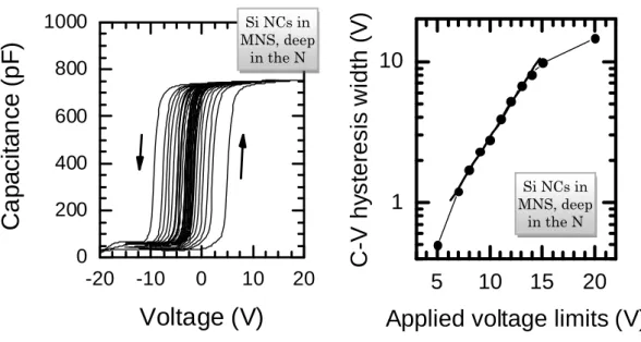
5.1C−V HYSTERESIS ... 63
5.2MEMORY WINDOW ... 67
5.2.1 Variation of the charging voltage pulse amplitude ... 67
5.2.2 Variation of the charging voltage pulse duration ... 73
5.2.3 Position of the flat-band voltage as a function of charging pulses ... 76
5.2.4 Total injected charge ... 79
5.3RETENTION ... 80
5.4CONCLUSIONS ... 83
SUMMARY ... 84
UTILIZATION OF THE NEW SCIENTIFIC RESULTS ... 86
LIST OF PUBLICATIONS ... 87
REFERENCES ... 89
LIST OF USED ACRONYMS ... 97
ACKNOWLEDGEMENTS ... 98
Preface – motivation and objectives
iv
Preface – motivation and objectives
Nowadays semiconductor (Si, Ge, etc.) nanocrystals embedded in dielectrics are intensively studied. One of the main goals of the researches is the exchange of conventional flash memories by nanocrystal-based flash memories.
Floating gate field effect devices are the basis of today's nonvolatile memory technology, such as the “flash” memory chips that are widely used as the data storage media in stand-alone (pen drives, memory sticks, MP3 players, PDAs, hybrid hard disks, etc.) or embedded applications (in automobiles, microcontrollers, appliances, wireless devices and other industrial controls). Information storage in these conventional semiconductor based non-volatile memories is based on the change of the threshold voltage in the case of metal-insulator-semiconductor (MIS) field-effect memory transistors, due to appropriate charging voltage pulses. During writing, charge carriers tunnel through the tunneling layer to the floating gate, or to the defects in the dielectric where they are stored.
The presence or absence of this charge corresponds to the logical 0 or 1 states.
In accordance with the fast size shrinkage as described by Moore's law, there is an urgent need for device elements with reduced lateral dimensions, on one hand. On the other hand, protection of charge leakage from the floating-gate requires thick tunneling oxides. It implies large charging voltages that need switching circuits with large lateral sizes and hence, it is an important limitation against satisfying Moore's law. According to the 2007 edition of the International Technology Roadmap for Semiconductors, the area required for the storage of one bit information in the case of a conventional memory cell, will be 24 percent of the 2007 value 652 nm2 in 2013, while the thickness of the SiO2 layer stagnates around 8–9 nm [0−1]. This implies an increased importance of switching circuit areas which meanwhile remains the same as bottom SiO2 layer thickness does not scale down. This is a serious technological issue, which needs to be solved.
Using semiconductor nanocrystals, charge is stored in particles separated from each other by wide band-gap dielectrics. This increases reliability because a single nanocrystal cell does not lead to complete charge loss as through an occurring defect in the case of a conventional floating gate. The use of nanocrystals is thus expected to be a promising alternative to the present floating gate technology. The conclusion, that it is a valid solution for the limitation issues of conventional technology, is confirmed by the fact that IBM reported the first nanocrystal memory device in 1996, and this was followed by Motorola’s demonstration of a 4 Mbit Si nanocrystal memory device in 2003.
v
The main objective of my Ph.D. work was the experimental study of the preparation and operation of metal–insulator–semiconductor (MIS) capacitance structures with embedded Si or Ge nanocrystals. The preparation of such structures involved low-pressure chemical vapour deposition, electron beam evaporation and nitric acid oxidation (the latter was applied to Si nanocrystals for the first time). The size, density and location of these nanocrystals was varied to optimize the memory properties (charge injection and charge storage). Size-dependent structural parameters on the nanocrystalline structures (mainly the nanocrystal size, density and separation, and the thin film thickness and composition) were determined by a variety of investigation methods, such as spectroscopic ellipsometry, cross-sectional transmission electron microscopy (XTEM), atomic force microscopy (AFM), scanning electron microscopy (SEM), X-ray photoelectron spectroscopy, and sheet resistance measurements.
Intensive research in recent years enabled the embedded nanocrystal structures to become suitable for the low charing voltage needs (below 10 V) of the non-volatile industry.
However, numerous physical aspects of the device operation is still not clear: e.g., whether the charge is stored in quantum states of a nanocrystal quantum box or in defect states at the nanocrystal/dielectric interface. There is only scant data about the charge distribution in the layer in the presence of nanocrystals as well. My contribution to the topic was, on one hand, the electrical memory investigation of such structures, as a function of structural parameters of the embedding layers and the nanocrystals, and on the other hand, the structural investigations of nanomaterial systems, which itself bears also important challenges. For example, the absence of reference dielectric spectra for the optical models of nanocrystalline materials is a considerable deficiency. That is why spectroscopic ellipsometry was applied for the parametric composition of the dielectric function of nanocrystalline silicon.
My motivation in this work was to contribute to this topic with new designs of structures, deep investigation of nano-material properties, and optimization of the structure design according to electrical memory qualifications.
This Ph.D. thesis is organized as follows:
Chapter 1 presents a classification of electronic memories and an introduction to the preparation and to the memory application of embedded Si and Ge nanocrystals in dielectric layers.
In Chapter 2, the preparation methods used in this work for both the nanocrystals and the dielectric layers are described. The design considerations and the summary of prepared samples is also discussed here. This is followed by Chapter 3, which summarizes the applied investigation methods including the optical models for spectroscopic ellipsometry, and the method of memory measurements.
Chapter 4 discusses the main results of the structural investigations of the studied structures. The results of cross-sectional transmission electron microscopy, X-ray
Preface – motivation and objectives
vi
photoelectron spectroscopy, atomic force microscopy, scanning electron microscopy, spectroscopic ellipsometry, and the sheet resistance measurements are summarized here.
Finally, in Chapter 5, the main results of the memory measurements are discussed, including the results of the capacitance–voltage hysteresis, the memory window, and the charge retention measurements.
1
Chapter 1 – Introduction to non-volatile memories
1.1 Classification of electronic memories
Semiconductor memories are essential elements of present day electronic devices.
Such devices are used in pen-drives, memory cards, MP3 players, personal digital assistants (PDAs), general positioning system (GPS) and robotic systems or in mobile phones. Commercially available electronic memory devices (and also those that are under development) can be distinguished by some basic properties which are the following.
1. Volatility. Volatile memories lose information if they loose power, while non- volatile memories store information without supplying power. The two most common volatile memory types are dynamic random access memory (DRAM) and static random access memory (SRAM). DRAM needs to be periodically refreshed, while SRAM keeps information without any refreshment until power remains applied. They typically need low programming voltages (around 1 V) with ultra-small times required for programming (in the range of 10–50 ns) [0−1]. Non-volatile memories need higher programming voltages (in the range of 7-19 V) with a wide range of reported programming times, between 50 ns and 100 ms [0−1].
2. Method of information storage. As volatile memories are off-topic to present subject, only non-volatile memories are dealt with in the following. Among non-volatile memories, a variety of used information storage mechanisms exist.
2.a. Non-charge-storage memories
– Ferroelectric memories (FRAMs) use ferroelectric layer as a dielectric inside a capacitor for information storage. They need small and short programming voltage pulses like volatile memories, and indeed, in construction they are similar to DRAM. This memory technology features advantages of high-speed data read/write functions, low power consumption, and virtually unlimited read/write cycles [1−1].
– Magnetoresistive memories (MRAMs) also use a capacitor in the memory cell but the ferroelectric element is not in the dielectric, but in the plates instead.
They also need low and short voltage pulses for programming [1−1].
– In the case of phase-change memories (PRAMs) the phase of a channel is switched by voltage pulses between nanocrystalline and amorphous state (that corresponds to high and low conductance, respectively). The best published programming voltage pulse amplitudes are extremely low (below 1 V) and the required pulse width is also in the range of 50 ns. Phase-change memories are widely thought to be the final alternatives to replace present- day non-volatile memories, and to become the “ultimate memory”. However, if using as devices, more dramatic change is needed for them in the technological process comparing to present-day flash memory structures, than
Chapter 1 Introduction
2
for nanocrystal flash memories. Nevertheless, nanocrystal flash memories seem to be a good temporary solution until phase-change technology reaches the level demanded by solid-state manufacturers. [1−1]
2.b. Charge-storage memories
– The Electrically Erasable Programmable Read Only Memory (EEPROM) was introduced in the early 80’s. Unlike its earlier version, EPROM, it can be reprogrammed by applying an electrical voltage. As a matter of fact, EEPROM is erased and reprogrammed at the individual cell level. While this results in high functionality which makes it well suited to particular applications for program memory of embedded systems, EEPROM devices are generally less cost-effective and are slower to program and erase than flash memory devices. However, they are ideal for the storage of firmware code because of the possible access at the byte-level. [1−1]
– The flash memory is currently the largest segment of the non-volatile memory market and is similar to EEPROM in that it can also be erased and reprogrammed repeatedly through the application of an electrical voltage.
Flash memory cells can be erased in blocks by a single action or “flash”, which makes it cost far less because of the simplified design, than EEPROM. Their programming voltage amplitudes are currently typically between 7 and 19 V.
[0−1,1−1]
1.2 Materials and methods of preparation
A silicon nanocrystal based memory structure was first suggested and published by Sandip Tiwari et al. from IBM Research Division, in Applied Physics Letters on 4th March 1996 [1−2], which became the most cited article ever published on this subject. His group realized an n-channel silicon FET with a sheet of Si nanocrystals (NCs) distributed in a silicon dioxide film, above the channel. They used a very thin tunneling oxide (1.1–1.8 nm) and a thicker control oxide above the NCs (4.5 nm or thicker).
NC-based electronic non-volatile memory structures are prepared by four main methods, that are described in this chapter. These are: the ion-beam synthesis, the layer- by-layer growth, the non-stoichiometric layer deposition and the CVD method.
From the application point of view, the ideal NC size, density and position inside the dielectric medium is crucial. It is important to position the NCs to a 2-3 nm distance from the Si substrate, on top of a good quality SiO2 to enable direct tunneling from the substrate to the NCs. The Si/SiO2 interface must be as perfect as possible to minimize the density of trap sites on the interface and to avoid its influence on the formation of accumulation and inversion layer during application of voltage to the device.
On one hand, the NC size must be larger than 3–4 nm because of the effect of charge confinement, namely: the increase of energy levels when more than one electrons are stored. This would badly affect charge retention characteristics since the potential
3
barrier for the electron occupying the highest energy level would decrease in this case comparing to NCs with larger size as the energy level separation increase according to the following equations [1−3]:
2 (Eq. 1−1)
, 1 · (Eq. 1−2)
where d is the diameter of a spherical NC, is the capacitance of a spherical NC and Δ , is the separation between energy levels inside the NC.
On the other hand, NC density at least 1012 cm–2 is required to minimize statistical variations. As the typical separation of NCs must be greater than 4 nm (to minimize lateral tunneling between NCs), NC size around 5 nm could be optimal. [1−3] An additional requirement for the NCs is that their size distribution must be narrow enough to avoid statistical effects which block further application in real memory devices.
1.2.1 Ion beam synthesis
The most frequently used method is the ion beam synthesis, which means implantation of Si or Ge into a SiOx layer with ultra-low-energies and subsequent annealing (or oxidation) at high temperatures. In the next few paragraphs, some examples of recent and typical achievements are summarized. A comprehensive list of publications in such subject is available on http://www.cemes.fr/neon.html that is the homepage of a former EU project called NEON (Nanoparticles for Electronics).
Si nanocrystals
Formation of Si NCs takes place after implantation typically with dose of 1015–1016 ions/cm2. The size of the NCs can be controlled between approximately 2–15 nm by adjusting the post-annealing temperature around 1000OC. A few examples from the literature are described below.
Normand et al. [1−4,1−5] implanted Si+ ions at 1 keV with a dose in the order of
~1016 ions/cm2 into 7–8 nm thick thermal SiO2. They observed Si nanoclusters with sizes in the range between 4–14 nm by TEM depending on the annealing temperature, which was ranging from 900OC to 1000OC for 30 or 60 min in N2.
Heinig et al. [1−6] implanted their 15 nm thick thermal SiO2/Si structure with Si+ ions at 50 keV with a dose in the order of ~3·1015–1016 ions/cm2. They predict Si NCs with 2–3 nm diameter by Monte-Carlo simulation, however, they did not observe them with XTEM because of the too small size. Their annealing procedure was executed at temperatures between 950–1100OC and times between 5–180 sec in inert ambient. Both authors suggest that Si NC formation takes place basically because of phase separation of Si and SiO2 during annealing.
Chapter 1 Introduction
4
Ge nanocrystals
In the case of Ge NC formation, doses between 1015–1017 ions/cm2 are typically used.
The post-annealing temperature needed to form the nanoparticles is somewhat lower than in previous case, here it is around 600OC. Two typical experiments are reviewed below.
Tsuji et al. [1−7] implanted Ge– ions at 10 keV with a dose in the order of (1–5)·1015 ions/cm2 into 12 nm thick thermal SiO2. They observed Ge nanoparticles with sizes in the range between 2–5 nm by cross-sectional transmission electron microscopy (XTEM) depending on the annealing temperature and implantation flux, which was ranging from 300OC to 900OC for 60 min in vacuum. They found that thermal diffusion of Ge atoms in SiO2 is notable in the case of annealing at 900OC, however, it was negligible at 300OC.
Masuda et al. [1−8] implanted Ge+ ions at 8 keV (low energy implantation, LEI) or 50–360 keV (high energy implantation, HEI) with a dose in the order of 1016–1017 ions/cm2 into thick SiO2 films. They observed Ge nanoparticles with 4.5 nm average diameter in the case of HEI and 5.2 nm in the case of LEI by transmission electron microscopy (TEM). The annealing was executed with temperature of 600OC for 30 min in N2. They found by Rutherford backscattering spectrometry (RBS) that there is no significant compositional difference between the as-implanted sample and the annealed sample.
Si and Ge nanocrystals
Unexpectedly, both Si and Ge NC formation were observed by Giri et al. [1−9] with Ge implantation only, after annealing at higher temperatures, between 800 and 950OC.
Giri et al. [1−9] implanted Ge+ ions at 300 keV with a dose in the order of 3·1016–2·1017 ions/cm2 into 250 nm thick thermal SiO2. They observed both Si and Ge nanocrystals after annealing in argon at 800OC and 950OC for several hours. Ge NCs sizes were found to vary between 4 and 13 nm estimated from Raman scattering data depending on annealing temperature and implantation dose. They obviously found that increasing the annealing temperature results in the increase of NC size. They estimate the average size of Si NCs which were identified by optical Raman spectra, for 8 nm by XRD, however, they expect that Si NC sizes are smaller than that of Ge's because of smaller Si concentration present in the layer.
1.2.2 Layer by layer growth
Another method is a layer by layer growth, i. e., the deposition of a thin amorphous or polycrystalline Si or Ge layer onto a lower dielectric (SiO2, Si3N4, etc.) layer. This Si or Ge layer is either covered by another dielectric layer, or the Si grains themselves are oxidized. The nanocrystals are formed by annealing either during evaporation, after the deposition of the Si or Ge layer, or after the deposition of the second dielectric layer.
Such structure was prepared by Kobayashi et al. [1−10] who evaporated a thin, 10 nm thick Ge layer onto a 4-nm-thick thermal SiO2 by e-beam evaporation at a substrate
5
temperature of 60OC at 10-7 Torr high vacuum. The sample was then annealed at temperatures between 800 and 1000OC in O2 atmosphere. Due to this high temperature oxidation, the Ge became oxidized and formed NCs with average sizes of 5 nm as obtained by modeling the measured Raman line shape. They monitored the Ge position by secondary ion mass spectrometry (SIMS) after oxidation and found that Ge stays on top of the bottom oxide in the case of oxidation at 800OC, while oxidation at 1000OC caused diffusion of the Ge content to the interface of Si/SiO2.
Note, that it is in correspondence with the result found by Tsuji et al. [1−7]
described above, who found that diffusion of Ge atoms is notable in the case of annealing at 900OC.
However, another article reports different result. Shklyaev et al. [1−11] published that e-beam evaporation of Ge onto thin SiO2 covered Si substrates with growth temperatures between 320 and 430OC results in Ge island growth on the SiO2 layer, while growth temperatures between 430 and 600OC drive different mechanism. At this temperature regime, epitaxial growth takes place on the a-SiO2 layer which can be possible if the Si surface becomes visible for the incoming Ge atoms. It means that part of the oxygen content of the SiO2 leaves the Si surface as SiO and GeO. This is partly in contradiction with the statement in previous article, namely, that Ge stays on the surface of thin SiO2 at oxidation temperatures around 800OC. As a matter of fact, this temperature is far higher than 600OC, but the ambient is O2 in that case that could be responsible for the absence of oxygen reduction of SiO2 by Ge. Another point is that in former case the thickness of the evaporated Ge layer was around 10 nm, while Shklyaev et al. deposited Ge layers with thicknesses between 1–7 monolayers.
Another article reports several temperature dependant pathways for the Ge species on SiO2 [1−12]. Based on this, for temperatures above 500OC, the following three-step process is suggested for the Ge to evaporate:
1.
2. 2
3. .
In summary, as a result of high-temperature treatment, Ge nanoparticles on thin SiO2 layers either diffuse to the interface of Si/SiO2 or leave the solid phase as gaseous GeO.
1.2.3 Non-stoichiometric dielectric layer deposition
The third method is the deposition of a Si-rich or Ge-containing SiOx or SiNxlayer, and formation of nanocrystals within the SiOx or SiNxlayer by high temperature annealing [1−13].
As an example of this method for formation, I would mention the work of Iacona et al. [1−13] who used PECVD to deposit Si-rich SiO2 films. They found NC formation due to high temperature annealing (between 1000–1300OC). Transmission electron microscopy (TEM) study revealed NCs with mean diameters between 1.4 and 4.2 nm.
Chapter 1 Introduction
6
1.2.4 Direct CVD growth
The fourth, most recent method is the deposition of Si nanocrystals themselves or of a SiNx layer containing Si nanocrystals by different chemical vapor deposition (CVD) methods. An important point is the control of initial nucleation of Si NCs on top of SiO2.
Brunets et al. [1−14] create reactive surface sites on the oxide by changing the surface Si–O bonds with Si–OH (silanol) bonds with the use of a solution of 0.3% HF and 0.3% HCl. Silanol bonds have significantly lower dissociation energy which means that the incoming Si atoms could more easily break the silanol bond and bond to the SiO2. The same method was applied by Baron et al. [1−15], however, Rao et al. [1−16] did not use similar procedure.
Brunets et al. [1−14] deposited Si NCs by LPCVD on top of 2.5 nm thick SiO2
covered Si substrates at temperatures around 300OC using disilane and trisilane source gases. The nanocrystal formation took place directly during deposition and their typical diameter was found to be around or below 5 nm. Finally, the samples were covered with atomic layer deposition (ALD) of Al2O3.
Baron et al. [1−15] also used LPCVD for the formation of Si NCs but with silane and dichloro-silane as input gases. They proposed a two-step model for the CVD process:
first, a nucleation step takes place with the introduction of silane to the system, and second, the growing of Si nuclei with dichloro-silane as precursor. They obtained a direct correlation between deposition time of the second step (0–50 min) and Si NC size (0–30 nm) by atomic force microscopy (AFM) measurements.
Rao et al. [1−3,1−16] used LPCVD for Si NC deposition on SiO2 covered Si substrates and obtained Si NCs with sizes around 5 nm and density of 1012 cm–2.
Sung et al. [1−17,1−18,1−19 used PECVD to deposit embedded Si NCs in amorphous SiNx layers with total pressure, plasma power, and growth temperature around 0.5 Torr, 5 W, and 250OC, respectively. They observed Si NCs with diameters between 2.6 and 6.1 nm as varying the deposition parameters. No annealing was required for the NC formation.
Wan et al. [1−20] used LPCVD to directly deposit Si NCs with a silicon nitride shell (they refer to the structure as SiN »silicon nitride« dot). They use LPCVD with dichloro silane (DCS) and ammonia (NH3) at 725OC and DCS/NH3 ratio of 1/5 and found that during initial stage of stoichiometric Si3N4 deposition, the layer is not continuous and Si-rich. As nitride growth begins with creation of Si-to-Si bonds, they explain slower growth on silicon oxide substrates than on silicon substrates. They interrupted the deposition at a certain time and expected that Si nanodots would not be continuous laterally, surrounded by silicon nitride shells.
7
1.3 Memory characterization of flash memory structures
1.3.1 Principles of operation
Information storage in conventional flash memories is based on the change of threshold voltage of field-effect transistors (FETs) by appropriate voltage pulses. During writing to the device, charge carriers tunnel to the “floating gate” where they are being stored. Reading procedure is based on applying a low voltage to the gate of the FET and check by measuring the source-drain current whether it is opened. Future applications such as the use in notebooks instead of hard disks require smaller and faster memory device elements which operate with lower voltages. However, the reduction of dimensions is limited in the case of conventional flash memories. Replacing the continuous floating gate by isolated nanocrystals is a possible new technology, which replaces conventional devices.
A schematic of a nanocrystal-based flash memory transistor is shown in Fig. 1−1. In the case of leakage, only a part of nanocrystals would deplete and the information is retained.
It implies the possibility of smaller voltage pulses, as smaller charge amount is enough to be present in the layer to provide reliable information storage.
S. Tiwari et al. [1−2] describe the information storage mechanism in such device as follows. The injection of electrons takes place by direct tunneling from the inversion layer to the NCs by applying reverse bias to the gate. As a consequence, the stored charge screens the gate charge that results in the reduction of conductance in the inversion layer, i.e., it effectively shifts the threshold voltage of the device. They suggest a device with NC sizes of 5 nm with separation of 5 nm (corresponding to density of 1012 cm–2), and top oxide thickness of 7 nm. With this structure, the threshold voltage shift is around 0.3–0.4 V for one electron per NC whose effect can be easily detected by source-drain current measurement. The Coulomb blockade energy for such NC is around 74 meV that is on one hand, larger than the room temperature thermal energy, and on the other hand, enables multi-electron storage in a single NC.
It is essential to minimize the writing/erasing (W/E) voltage amplitudes of the devices. So, a key issue is the optimization of the structure for maximizing the injection current at a given gate voltage. The injection current is essentially an exponential function of the electric field in the bottom dielectric layer [1−21]. The bottom dielectric layer is often referred as the tunneling layer, or the tunneling oxide layer (in most cases, it is a SiO2 layer on top of the Si substrate). The electric field in this tunneling layer is a function of the thickness of this layer, the thickness of the top dielectric layer, the dielectric constants of both layers, and the trapped charge in both layers. When no charge is stored in the structure, the electric field in the tunneling oxide layer is given as
·
·
, (Eq. 1−3)
where is the gate voltage, and are the dielectric constant and the thickness of the bottom oxide layer, respectively, and and are the dielectric constant and the
Chapter 1 Introduction
8
thickness of the top layer, respectively [1−21]. This suggests that the decrease of the ratio increases the oxide field, and this increase is independent of the gate voltage.
Practically, this means that the dielectric constant of the top dielectric layer should be larger than that of the bottom layer. Such a case is achieved in metal-nitride-oxide-silicon (MNOS) structures, because the dielectric constant of the Si3N4 is between 6.9–7.5, while the dielectric constant of SiO2 is around 3.9 [1−1].
Fig. 1−1. Flash memory transistor with nanocrystals
The energy band diagram during charge injection for a MNOS capacitor with Si nanocrystals is shown in Fig. 1−2. Charge is injected from the accumulation layer in the substrate to either the NCs or to defect sites (traps) located in the Si3N4 layer by tunneling.
Direct tunneling takes place if the underlying oxide layer is sufficiently thin enough (~3 nm).
After injection, the total stored charge in the nitride layer is given by
· , (Eq. 1−4)
where q is the elemental charge, is the spatial distribution of charge, and and are positions in the layer, as shown in Fig. 1−2. In the case of calculations for metal- oxide-semiconductor (MOS) structures, it is often approximated that the stored charge is located at the Si/SiO2 interface, because the function is usually not known. However, for charge trapped in MNOS structures, the charge centroid is defined [1−22,1−23,1−24,1−25] which describe this distribution by the position of the centroid in the nitride. It is generally defined as
· · , (Eq. 1−5)
where xc is the distance of the charge centroid from the Si/SiO2 interface, and is the total stored charge in the layer.
channel
source drain
gate
silicon
top dielectric layer nanocrystals
bottom dielectric layer
9 Si
~5.1 eV
Si3N4 Al
~3.1 eV ~1.05 eV
Si NC
~9 eV
SiO2
nanocrystal gap
q·Voxide
q·Vnitride
0 xoxide xnitride
x
Fig. 1−2. A schematic of the energy band diagram during charge injection for a MNOS capacitor with Si nanocrystals
The flat-band voltage in metal-insulator-semiconductor (MIS) devices is the voltage at which there is no electrical charge in the semiconductor and, therefore, no voltage drop across it; in the band diagram the energy bands of the semiconductor are horizontal (flat) [1−26]. The flat-band voltage in an MNOS structure is generally given by
, (Eq. 1−6)
where is the work function difference between the metal (usually Al, or poly-silicon) and Si, is the density of charge (per unit area) stored in the nitride layer (including the NCs) with thickness , is the charge density in the oxide, if it is at the Si/SiO2
interface, is the oxide thickness, and and are the dielectric constants for the nitride and the oxide layer. However, in practice is negiligible and the corresponding term can be neglected. Consequently, the flat-band voltage shift caused by the injected charge density Δ in the nitride layer (including the NCs) is then given as
, (Eq. 1−7)
This means increased effect of the trapped charge on the memory window width if it is located closer to the substrate (it is characteristically at the SiO2/Si3N4 interface if equals zero). As NCs (representing large density of traps) are formed directly at the SiO2/Si3N4
interface (in the case of MNOS structures), improvement of the memory window is expected for MNOS samples with embedded NCs, with respect to MNOS reference samples (without the NCs).
Chapter 1 Introduction
10
In the case of structures where only NCs are considered to store the charge (e.g.
NCs embedded in SiO2), if only one electron per NC is assumed, the following equation is obtained (by deriving Poisson's equation in an oxide) for the resulting flat-band voltage shift [1−27,1−28,1−29]:
· · ∆ , (Eq. 1−8)
where is the effective dielectric constant of the nanocrystal, is the diameter of the NCs, and is the thickness of the oxide layer above the NCs.
Combining Eq. 1−7 and Eq. 1−8, in the case of MNOS samples with embedded NCs in the nitride close to the SiO2/Si3N4 interface, the following relation is obtained:
∆ · · ∆ · ∆ , (Eq. 1−9)
where is the density of charge stored in the nitride only (excluding the NCs).
During charge storage in our case, the single MIS capacitor device is separated from the charging circuit by a relay immediately when the charging voltage returns to zero.
Then discharge phenomena occurs by tunneling from either the NCs or the nitride traps backwards to the substrate or in forward direction, towards the top electrode. The discharge current is strongly determined by the barrier height for the tunneling carriers which is a definite function of the NC size [1−30], by the density of the NCs, and by the total stored charge [1−29]. The amount of charge stored in the device [1−29,1−32] is given as
· (Eq. 1−10)
0 · , (Eq. 1−11)
where is the transition probability of a charge carrier from a trap state to the substrate, which is given as
· · · . (Eq. 1−12)
Here, is the density of states, is the transmission probability across the bottom oxide, is a temperature-dependent factor, contains the geometry, and the semi- classical escape attempt rate for NCs, which is given as
. (Eq. 1−13)
Here, is the effective electron mass in the nanocrystal, and is the NC diameter [1−29,1−31].
11
1.3.2 Definition of the memory window
The written state of a memory capacitor structure is defined by its flat-band voltage after the application of a high voltage pulse (where “high” means higher than the voltage used during the “read” procedure) to the structure. The erased state is defined by the flat- band voltage after the application of an opposite voltage pulse. The memory window width of a memory element is defined by the flat-band voltage difference between the written and the erased state. The position of the memory window is defined as the value of the flat-band voltage.
1.3.3 Definition of the retention
Basically, the charge retention of a structure is given by the change of its flat-band voltage after a single W/E voltage pulse, as a function of waiting time. The retention is often characterized by the extrapolated value of the memory window width for 1 or 10 years. This extrapolation is based on the exponential time dependence of the amount of charge in the device (see Eq. 1−11).
1.3.4 Recent results
Recent results reported on memory devices with Si nanocrystals prepared by ultralow-energy ion-beam synthesis are promising [1−5,1−33]. It was obtained that the memory behavior of the devices prepared by this method does depend not only on the implantation (energy and dose) and annealing (temperature, time, ambient) parameters, but also on such effects and circumstances, as contamination and electrical charging of the sample surface during implantation, oxide swelling, cleaning procedure before annealing, and the energy contamination [1−5].
Optimizing the above parameters, memory transistors with the following characteristics were obtained by Normand et al. [1−5]. About 2 V memory window width was obtained for W/E pulses of ±9 V, 10 ms. No change of the memory window was detected after 1.5 million W/E cycles (stress). The extrapolated memory window of unstressed devices kept at 85OC is 0.4 V after 10 years, it means that the memory window decreased to
~20% of its initial value. The stressed devices also store the information for several years.
In another recent work of Ng et al. [1−33] memory window width of about 1 V has been achieved by writing/erasing pulses of ±12 V, 1 μs on devices prepared also by ultra- low-energy ion-beam synthesis. The extrapolated memory window width after 10 years is about 0.3 V.
Another important result is the realization of MOS memory FETs with Si nanocrystals feasible for dual bit storage of information [1−34]. In another work the effect of single electron charging on the drain current was demonstrated and studied in detail [1−35].
Chapter 1 Introduction
12
1.3.5 Recent solutions on the market
Since Freescale Semiconductors (a spinoff company of Motorola) introduced a 4-Mbit nanocrystal flash memory in production in 2003, and a 24-Mbit array in 2005 [1−36,1−37], development effort in nanocrystal memory cells is ongoing with at least 5 of the top 10 flash memory suppliers [1−38].
Developers and vendors of nanocrystal memories include among others Atmel, Freescale (Motorola), IBM, Renesas, Toshiba, or Hitachi. According to an analysis, the flash memory market (with the conventional floating-gate flash memory transistors) is expected to double between 2005 and 2009, worldwide [1−39]. A recent report in Hungary revealed that the growth of the local flash memory market doubled from 2006 to 2007 [1−40].
Freescale
This company has created the world's first 24-Mbit memory array using 90 nm CMOS bulk technology. They state that the production of a working 24-Mbit memory device requires that silicon nanocrystals be deposited with good uniformity and integration approaches that keep the nanocrystal properties intact during subsequent processing. In successfully achieving this, Freescale has overcome major challenges to introducing this technology into production.
They created nanocrystal memory cells by forming a layer of 5 nm silicon dots, deposited on a 5 nm grid on top of the thin gate oxide layer. Another oxide layer is deposited on top of the nanocrystal layer, and then the polysilicon gate is formed on top of the oxide. As the tunnel oxide under the nanocrystal layer can be scaled down, reducing the voltage needed for program/erase operations: 8 to 10 V, as opposed to the 12 to 15 V used for most floating-gate storage cells.
Atmel Corp.
Atmel has an on-going R&D project for next generation non-volatile memories, called Erevna. The overall objective of this project is to develop flash memories with embedded silicon nanocrystals at the 130-nm, 90-nm, and 65-nm nodes, for use up to the year 2009. [1−41]
Spansion
The company Spansion was founded as a result of agreement between Fujitsu and AMD in 1993. It is currently one of the largest vendors of flash memory devices. However, there is no data about its production of nanocrystal flash memories, its fellows publish scientific results about the subject in the literature [1−42,1−43].
Other companies
Members of staff of the other big companies, such as Hitachi [1−44], IBM [1−45] or Toshiba [1−46] are also publishing on nanocrystal flash memories, however, there is no data available about implementing their results into production.
13
1.4 Conclusions
In this chapter, a brief introduction was given into the subject non-volatile memories. A grouping of electronic memories was presented, from the view-points of volatility and method of information storage. Common materials and methods of preparation were reviewed, with a comparison between different observations in the literature. Emphasis was taken on the formation of Si and Ge nanocrystals in dielectric layers. Memory qualification methods of flash memory structures were shown, with the principles of operation. The theoretical background for charge storage is introduced. The definition of the memory window and the retention was explained. A summary of recent flash memory products with nanocrystals was showed.
Chapter 2 Methods of preparation
14
Chapter 2 – Methods of preparation of the studied structures
2.1 Introduction
The experimental procedures used in this work are described for different layer depositions, and for the formation of Si or Ge nanocrystals in the followings.
2.2 Preparation of thin layers
2.2.1 Silicon nitride layers
Low-pressure chemical vapor deposition (LPCVD) method provides a trustworthy way of depositing electrically insulating silicon nitride thin layers. However, other methods such as sputtering or plasma-enhanced chemical vapor deposition (PECVD) exist, these are not operated at low pressures, low activation energies, or the reagents are too large during deposition, and hence, the resulting layer is not dense nor defect-safe enough to provide low leakage currents during electrical applications.
In this work, the setup used for the deposition of silicon nitride thin layers was a software-controlled Amtech-Tempress LPCVD device. It operates at 30 Pa pressure and a temperature of 810OC is used regularly for silicon nitride processing. The silicon nitride layers are formed on top of (100) oriented Si wafers as introducing SiH2Cl2 (dichloro-silane, or DCS) and NH3 into the heated quartz tube according to the following equation:
. (Eq. 2−1)
The stoichiometric layers were grown with gas flow rates of DCS to NH3 of 21 to 90 sccm, respectively. For non-stoichiometric layers, the DCS to NH3 ratio was increased.
The thickness of the layer was controlled by the deposition time and verified by spectroscopic ellipsometry measurements on reference samples. The obtained deposition time vs. thickness data is plotted in Fig. 2−1. The actual growth speed of the layer is found to be around 3.9 nm/min below 10 min, and around 1.6 nm/min above 10 min. The difference of layer growth speeds is probably connected with the relatively slow (around 30 sec) switch-on time of the DCS cock, that strongly affects the incubation time of the growth process. Later, the deposited layer thickness is clearly a linear function of the deposition time.
15
0 10 20 30 40
0 20 40 60 80
L a ye r t h ick n e ss ( n m )
Deposition time (min)
Fig. 2−1. Deposition time versus Si3N4 layer thickness in the case of LPCVD growth
2.2.2 Thin silicon dioxide layers
For the formation of thin silicon dioxide layers, a method by use of HNO3, as reported earlier by H. Kobayashi et al. [2−1] was applied after cleaning the (001) oriented n-type Si substrates in 1 wt% HF. Then, the n-type Si wafers were immersed in 68 wt%
HNO3 at the boiling temperature (121 oC) for 60 minutes. This method yielded a SiO2 layer with a thickness of 2.5 nm, as obtained by cross-sectional transmission electron microscopy (XTEM).
2.2.3 Thick silicon dioxide layers
Thick (~100 nm) SiO2 layers were formed either by thermal oxidation of Si or by atmospheric chemical vapor deposition of SiO2 with SiH4 and O2.
2.3 Preparation of nanocrystals
2.3.1 Si nanocrystals
Si nanocrystals were formed during LPCVD with single SiH2Cl2 input gas at 30 Pa pressure and temperature of 810OC. Thin layers of nanocrystalline Si were prepared with deposition times between 30 sec and 300 sec on Si3N4, SiNx and on SiO2 covered Si substrates. The initial expectation was, that below a certain deposition time, the resulting thin layer becomes non-continuous. Note, that it was one of the goals of the work for this thesis.
I suggest here a discrete definition of terms Si nanocrystalline layer and Si nanocrystals. In the followings, I mean a continuous layer of silicon with small crystalline grains (with grain sizes in the nano range) as a Si nanocrystalline layer (nc-Si). As for Si
Chapter 2 Methods of preparation
16
nanocrystals (Si NCs), I would call nanocrystals (with sizes in the nano range) that are separated from each other by a material other than Si.
It is emphasized here, that the size of Si nanocrystals could be reduced by post- oxidizing them by the application of above mentioned HNO3 oxidation method. It is expected, that the resulting layer would include Si nanocrystals surrounded by a SiO2 shell.
2.3.2 Ge nanocrystals
In the case of Ge nanocrystal formation, Si wafers covered with SiO2 or Si3N4/SiO2
layers were loaded into an oil free evaporation chamber (Varian VT-460), and the system was evacuated down to 1×10⁻⁸ Torr. Ge ingot of 99.999% purity was supported on a molybdenum plate, and it was evaporated using an electron gun, at an evaporation rate of 0.01-0.03 nm/s, at a pressure of 1×10⁻⁷ Torr. During evaporation, and for an additional 1 minute after this process, the substrate temperature was kept at 350°C. The temperatures were monitored by small-heat-capacity Ni-NiCr thermocouples, while the film thicknesses were measured by a vibrating quartz probe.
Two series of samples were prepared depending on the thickness of bottom oxide layer. For initial experiments, Si substrates with 100 nm thick thermal silicon dioxide were prepared and the Ge was evaporated with different duration on the top of this structure.
The second series of samples were prepared directly for memory purposes. It contained two types of thin chemical oxides and the two thinnest Ge nanocrystal layers based on the initial experiments.
As for the initial experiments, Ge nanocrystals were thermally evaporated with different evaporation times. Four different sets of samples were formed with 2, 4, 6 and 8 equivalent monolayers of Ge. During evaporation, the evaporated mass of Ge was monitored with vibrating quartz. (The term equivalent monolayer means the mass of a fully compact Ge layer.) After Ge evaporation, a part of the samples were covered with thick SiO2
for XTEM measurements, and referred below as Samples No. 1', 2', 3', and 4', respectively.
In the case of thin film growth from vapor phase three basic modes of the growth process may occur, depending on the principal interactions between atoms of the substrate and atoms of the deposit [2−2]. These are: (a) layer by layer growth (Frank-van der Merwe type [2−3,2−4]), (b) island growth (Volmer-Weber type [2−5]), and Stransky-Krastanov [2−6,2−7,2−8] growth, at which one or several complete monolayers are formed before NC growth.
In the case of SiO2 covered Si wafers studied in this work the top of the substrate is amorphous, so the Stransky-Krastanov type growth of Ge is excluded. The cohesion between germanium atoms is larger, than their adhesion towards silicon dioxide.
Consequently, island growth (Volmer-Weber type) occurs. No wetting layer can be expected, which means that the Ge dots (under a certain density) may be independent from each other. Their shape is determined by the surface tension of Ge, that results in distorted spherical type rather than dome like islands.
17
2.4 Preparation of the metallization
All samples characterized by memory measurements underwent an appropriate chemical treatment [2−9] followed by metallization with Al evaporation on both sides.
Samples with Si3N4 layers underwent an additional silicon nitride etch procedure on backsides, preceding the chemical treatment. The mentioned chemical treatment is as follows.
First, the samples were immersed into 1:1 solution of H2SO4 + H2O2 for 30 mins.
This was followed by 1:20 solution of HF + H2O for 1 min and another 1:1 H2SO4 + H2O2 for 15 mins. Note, that the first and the last step forms a thin chemical oxide on the backside of the substrate, while the middle step removes it.
Finally, capacitors with 0.8 x 0.8 mm lateral sizes were formed by Al evaporation on both sides, and photolithography and Al-etching on the front side. The thickness of the Al layer was 1 μm in all cases. No post-annealing process was performed.
The two contacts during measurements are either on one of the capacitor squares on the top of the sample, and the other is at the bottom.
2.5 Annealing in forming gas
Annealing in forming gas (95% N2 + 5% H2) was performed on selected samples at 1000OC for 1 or 3 hours.
Chapter 2 Methods of preparation
18
2.6 Design considerations and summary of prepared samples
My main goals in the Ph.D. work were as follows:
– to prepare Si and Ge nanocrystals arranged in a sheet;
– to embed the nanocrystals into dielectric thin layers;
– to investigate the physical properties of the nanocrystals (such as their size, density and lateral separation), as well as their optical functions, as a function of deposition parameters;
– to prepare metal–insulator–silicon (MIS) structures with embedded nanocrystals and to investigate their charge storage properties primarily with memory window and retention measurements, as a function of nanocrystal properties, and the position of the sheet of nanocrystals inside the dielectric layer.
For accomplishing these goals, the following main ideas were considered for sample structures:
Planned goal: Accomplished goal:
samples with uncovered nanocrystals
on top of SiO2/Si substrates Ge nanocrystals with different size on top of a SiO2 covered Si substrate
samples with nanocrystals with different size, density and separation, embedded into different dielectric layers at different depths
Ge nanocrystals with different size on top of a SiO2 / Si, covered by another SiO2 layer Si3N4/SiO2/Si structures containing Ge (with Si3N4 as the conver dielectric)
Si nanocrystals with different size and density on SiO2/Si, SiNx/Si and Si3N4/SiO2/Si substrates, covered by SiO2 or SiNx
the study of the effect of annealing Si nanocrystals embedded in SiNx covered Si substrates
Basic structural information of the studied samples is shown in Table 2−1 and 2−2.
Table 2−1 is dedicated to give a general idea of the prepared samples. Detailed description of the sample structures is shown in Table 2−2.
19
Table 2−1. Short description of the studied samples
Sample No. Short description of the sample These samples were prepared to study…
Methods of structural investigations
Memory properties investigated
? N1 …the dependence of the composition of
SiNx single layers on top of Si, as a function of the ratio of input gases during
LPCVD deposition.
ellipsometry No.
N2 N3 SRX
…the role of annealing on the composition of the top and bottom SiNx
single layers, and on the crystallinity of the middle nanocrystalline Si layer.
ellipsometry,
XTEM, XPS No.
NI000
…the effect of LPCVD deposition time on the size and density of the forming Si nanocrystals, embedded in Si3N4 layers,
deep in the nitride;
…the memory properties as a function of nanocrystal properties, in the case of
MNS structures.
ellipsometry,
XTEM Yes.
NI030 NI045 NI060 NI120 NI180 NI300
COA00 …the effect of LPCVD deposition time on the size, density and separation of the forming Si nanocrystals, embedded at the
Si3N4/SiO2 interface;
…the memory properties as a function of nanocrystal properties, in the case of
MNOS structures.
XTEM, XPS Yes.
COA30 COA60 COA300
G1
…the effect of evaporation time on the size, density and separation of the forming Ge nanocrystals on top of SiO2
layers.
AFM, SEM, Van der Pauw
No.
G2 G3 G4 G1’
XTEM G2’
G3’
G4’
O000 …the memory properties as a function of nanocrystal properties, in the case of MNOS structure with embedded Si and
Ge nanocrystals in the nitride, close to the N/O interface.
XTEM Yes.
G025 G050 O060 Q120
Chapter 2 Methods of preparation
20
Table 2−2. Basic structural information of the studied samples, with layer materials and layer thicknesses, as obtained by spectroscopic ellipsometry and cross-sectional
transmission electron microscopy
Sample No.
Layer structure
(layer materials and thicknesses – on top of the Si substrate) Bottom layer Middle layer(s) Top layer N1 SiNx, 100 nm, (DCS to NH3 ratio: 120/20)
N2 SiNx, 100 nm, (DCS to NH3 ratio: 140/20) N3 SiNx, 100 nm, (DCS to NH3 ratio: 200/20)
SRX SiNx, ~18 nm Si NC, ~17 nm SiNx, ~18 nm NI000 Si3N4, 40 nm
NI030 Si3N4, 15 nm Si NC, 2.2 nm Si3N4, 32 nm NI045 Si3N4, 15 nm Si NC, ~3.9 nm Si3N4, 32 nm NI060 Si3N4, 15 nm Si NC, 5.1 nm Si3N4, 32 nm NI120 Si3N4, 15 nm Si NC, 8.4 nm Si3N4, 32 nm NI180 Si3N4, 15 nm continuous nc-Si layer, ~15 nm Si3N4, 32 nm NI300 Si3N4, 15 nm continuous nc-Si layer, ~23 nm Si3N4, 32 nm COA00 SiO2, 2.5 nm Si3N4, 40 nm
COA30 SiO2, 2.5 nm Si NC (30 sec deposition time) Si3N4, 40 nm COA60 SiO2, 2.5 nm Si NC (60 sec deposition time) Si3N4, 40 nm COA300 SiO2, 2.5 nm Si NC (300 sec deposition time) Si3N4, 40 nm
G1 SiO2, 100 nm Ge evaporated for ~25 sec G2 SiO2, 100 nm Ge evaporated for ~50 sec G3 SiO2, 100 nm Ge evaporated for ~75 sec G4 SiO2, 100 nm Ge evaporated for ~100 sec
G1’ SiO2, 100 nm Ge evaporated for ~25 sec SiO2, 100 nm G2’ SiO2, 100 nm Ge evaporated for ~50 sec SiO2, 100 nm G3’ SiO2, 100 nm Ge evaporated for ~75 sec SiO2, 100 nm G4’ SiO2, 100 nm Ge evaporated for ~100 sec SiO2, 100 nm O000 SiO2, 2.5 nm Si3N4, 35 nm
G025 SiO2, 2.5 nm Si3N4,
2.5–3 nm Ge evaporated
for ~25 sec Si3N4, 35 nm G050 SiO2, 2.5 nm Si3N4,
2.5–3 nm Ge evaporated
for ~50 sec Si3N4, 35 nm O060 SiO2, 2.5 nm Si3N4,
2.5–3 nm Si NC, 5.1 nm Si3N4, 35 nm Q120 SiO2, 2.5 nm Si3N4,
2.5–3 nm Si NC, 8.4 nm* Si3N4, 35 nm
*The size of the NCs in this sample differs in horizontal and vertical direction.
2.7 Conclusions
Experimental procedures used in this work for different layer depositions and for the formation of Si and Ge nanocrystals were summarized. A complete list of the prepared samples is presented with their structural information.
21
Chapter 3 – Methods of investigation
3.1 Structural characterization
The thickness and composition of the Si3N4 and SiO2 thin layers in the structures were determined by cross-sectional transmission electron microscopy (XTEM), energy- filtered cross-sectional transmission electron microscopy (EFTEM), X-ray photoelectron spectroscopy (XPS), and spectroscopic ellipsometry.
The size, distribution and composition of the nanoparticles were determined by cross-sectional transmission electron microscopy (XTEM), energy-filtered cross-sectional transmission electron microscopy (EFTEM), X-ray photoelectron spectroscopy (XPS), atomic force microscopy (AFM), and scanning electron microscopy (SEM).
3.1.1 Transmission electron microscopy
Transparent samples for TEM were prepared by Ar ion milling. Images of the samples were taken in a Philips CM20 electron microscope operating at 200 keV and JEOL 3010 high resolution, 300 keV TEM, both measurements performed in MTA MFA.
Characteristic nanocrystal sizes were determined based on all the visible nanocrystals observed in these cross-sectional transmission electron microscopy (XTEM) images.
3.1.2 Atomic force microscopy
The AFM was performed with a Veeco Nanoscope E STM/AFM instrument in tapping mode using Si3N4 tips with 20 nm radius and 0.06 N/m deflection spring constant in MTA MFA. The AFM measurements were performed on samples with Ge nanocrystals on SiO2 covered Si substrates (on samples G1, G2, G3 and G4).
I define the surface coverage of NCs with the area occupied by Ge clusters divided by the total observed area. Practically, this value was obtained in AFM images with image processing. A threshold level value of 66.7% was applied for samples G1 and G2, and a value of 33.3% was applied for samples G3, and G4. The ratio of white and black pixels in these threshold images was assigned to the surface coverage. The threshold level value was lower for samples G3 and G4 than for samples G1 and G2 because of the increased surface roughness. As the average diameter of Ge NCs is known for each sample, one can obtain the surface density of NCs by dividing the area covered by NCs by the area of the disk corresponding to one individual NC. [BP−2]
Chapter 3 Methods of investigation
22
3.1.3 Scanning electron microscopy
The SEM images of samples with Ge nanocrystals on SiO2 covered Si substrates were taken by a LEO Gemini 1540 scanning electron microscope in MTA MFA.
3.1.4 X-ray photoelectron spectroscopy
X-ray photoelectron spectroscopy (XPS) measurements were carried out on electron spectrometer ESCALAB MK2 (VG) with Al Kα X-ray monochromatized source (hν = 1486.6 eV), performed by Surface Phenomena Researches Group (SPRG), Scientific Enterprise, Moscow.
The samples in initial state and after multistage Ar+ ion etching (used for obtaining information from various depths) were investigated. The investigations were carried out in vacuum of 1×10⁻⁸ Pa. X-ray photoelectron spectroscopy was used as for investigations of phase composition, chemical state of atoms, and electronic structure of Si nanocrystals. The XPS spectra were recorded with speed of 0.1 eV/s with 100 scans. The spectrometer was adjusted using Ag reference. The charge effect was suppressed by charge neutralizer, the flood gun EMU-50. The beam of low energy electrons (30−45 eV) is suitable for neutralizing the charge of insulating samples during long XPS investigations. The physical/technical conditions for electronic spectra acquisition were selected in the best way to provide energy resolution of the spectrometer better than 0.6 eV.
3.1.5 Spectroscopic ellipsometry
Woollam M88 (1.63–4.43 eV), Woollam M2000 (1.24–5.04 eV) and Sopra ES-4G (1.5–5.0 eV) ellipsometers were used for the spectroscopic ellipsometry measurements. The measurements were performed in MTA MFA and at the University of Szeged.
The structural model used for modeling the samples with nanocrystals consisted of three layers on top of a silicon substrate. Only the middle layer in this model was considered to consist the nanocrystals. The dielectric function of this layer was modeled either by the effective medium approximation mixture of known dielectric functions or by parametric approximation. The former permitted to examine the composition of this layer, while the latter enabled to study the dependence of the dielectric function on the nanocrystal size.
23
Optical models for the silicon nitride layers
Effective medium approximation with Si3N4 and excess silicon
The Bruggeman Effective Medium Approximation (B−EMA) model can be used as the optical model of non-stoichiometric layers [BP−6,BP−9]. It mixes the dielectric function of two or three constituent materials by varying their volume fractions in an isotropic matrix. The requirement for B−EMA is that the sizes of the constituents are in the range or less than the wavelength of the measuring light, but large enough to preserve the bulk dielectric functions of the reference materials used in the B−EMA calculations.
This model can be applied to obtain the dielectric function of SiNx layers, as well, by choosing stoichiometric Si3N4 [3−1] and silicon as the constituent materials [3−1,3−2,3−3].
However, the dielectric function of amorphous, polycrystalline, or crystalline Si are different, and consequently, different dielectric functions for the silicon component can be used. In our case, silicon is present in the amorphous form in the SiNx layer, as obtained by cross-sectional transmission electron microscopy [BP−9], therefore the dielectric function of the amorphous silicon [3−4] should be used. The equation for the B−EMA that has to be solved to determine the volume fractions of the components and the complex dielectric function of the layer is
· 1 · 0 (Eq. 3−1)
where (unknown) and (known) are the volume fraction and the dielectric function of the first component, respectively, (known) is the dielectric function of the second component, and ε (unknown) is the complex dielectric function of the effective medium film layer. The main advantages of this model are its simplicity and its ability to determine the N to Si ratio (stoichiometry) of a SiNx film. However, the EMA is a mathematical model which do not consider the atomic densities, so the volume fraction of Si (which is the primary parameter obtained from the fit) must be corrected in order to determine the stoichiometry, according to the following equation:
· . ·
· . · · . (Eq. 3−2)
where is the stoichiometry of a SiNx layer, is the volume fraction of silicon in the layer, in addition to the Si3N4 (that is the result of the fit), and the atomic densities for Si3N4 and Si were considered as 1.48·1022 molecules/cm3 and 4.99·1022 atoms/cm3, respectively [3−5].