Optoelectronic Properties of CuI Photoelectrodes
A ́ dám Balog,
†Gergely F. Samu,
†,‡,§Prashant V. Kamat,
§,∥and Csaba Janáky*
,†,‡†Department of Physical Chemistry and Materials Science, Interdisciplinary Excellence Centre, University of Szeged, Rerrich Square 1, Szeged H-6720, Hungary
‡ELI-ALPS Research Institute, Dugonics sq. 13, Szeged 6720, Hungary
§Department of Chemistry and Biochemistry, University of Notre Dame, Notre Dame, Indiana 46556, United States
∥Radiation Laboratory, University of Notre Dame, Notre Dame, Indiana 46556, United States
*S Supporting Information
ABSTRACT: Detailed mechanistic understanding of the optoelectronic features is a key factor in designing efficient and stable photoelectrodes. In situ spectroelectrochemical methods were employed to scrutinize the effect of trap states on the optical and electronic properties of CuI photoelectrodes and to assess their stability against (photo)- electrochemical corrosion. The excitonic band in the absorption spectrum and the Raman spectral features were directly influenced by the applied bias potential. These spectral changes exhibit a good correlation with the alterations observed in the charge- transfer resistance. Interestingly, the population and depopulation of the trap states, which are responsible for the changes in both the optical and electronic properties, occur in a different potential/energy regime. Although cathodic photocorrosion of CuI is thermodynamically favored, this process is kinetically hindered, thus providing good stability in photoelectrochemical operation.
P
hotoelectrochemical (PEC) methods hold the promise of uniting the functions of solar cells and electrolyzers, thus directly converting sunlight to fuels.1 At the same time, after almost five decades of research on different semiconductor systems (e.g., metal oxides and chalcogenides), the magic bullet to attack the problem is still to be found.2,3 Both new materials and new methods are needed to develop photo- electrodes with enhanced PEC performance. The recent wave of excitement triggered in the solar energy community by lead halide perovskites has generated an interest in employing halide-based semiconductors also as photoelectrodes.4−7 At the same time, chemical, electrochemical, and photoelectro- chemical corrosion remains a major issue that needs to be better understood and circumvented.8,9In this Letter, we show how in situ spectroelectrochemical measurements can contribute to the better understanding of the optoelectronic properties of CuI, a prominent member of the metal halide family. The choice of material was deliberate, as the optoelectronic properties of CuI make it a suitable material for thermoelectrics,10 flexible transparent p−n diodes,11 thin-film transistors,12 hole-transporting layers in solar cells,13,14 or even for photocatalytic CO2 reduction.6 Notably, the oxide counterpart (Cu2O, cuprous oxide) of CuI is frequently studied as a promising photocathode material for solar fuel generation.15,16 At the same time, it is prone to photocorrosion, which severely limits its applicability, unless some protection strategy is employed.17,18
There are examples in the literature where spectroelec- trochemistry provided valuable insights into the energetics, defect sites, and charge-transfer properties of semiconductors.
For example, the redox transformation of conjugated polymers (organic semiconductors) was investigated by applying the combination of two in situ techniques at the same time, to follow both spectroelectrochemical and conductance changes.19,20 As for inorganic semiconductors, the presence of electrons in the accumulation layer of TiO2 was probed through spectroelectrochemistry.21 The flatband potential of semiconductors can be conveniently estimated from the onset potential of the absorbance change.22 The difference in spectral response and onset potential can also be used to distinguish theflatband potential and trapping of electrons at the defect sites.23 Spectroelectrochemical diffuse reflectance spectroscopy is also appropriate to seek information on electron traps and distinguish different chemical species generated during photoexcitation of the semiconductor.24−26 As discussed above, the existing literature is oxide- (and especially TiO2) centric. However, there are precedent spectroelectrochemical studies on other nonoxide materials as well (e.g., CdSe,27 CsPbBr3,28 CuInS2,29 and Cu:ZnSe/
CdSe30). Here, we present how the combination of two methods can furnish new insights on the optoelectronic properties of CuI.
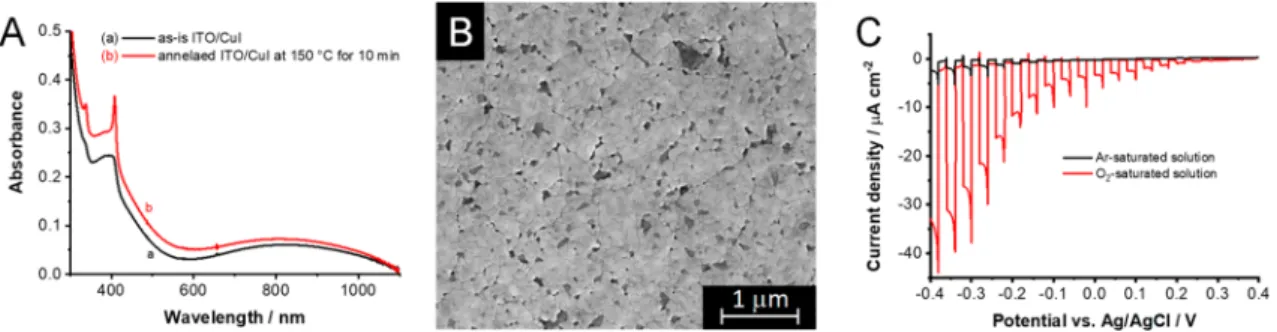
UV−visible spectra were recorded for the spin-coated CuI layers before and after annealing at 150°C for 10 min (Figure 1A). The annealed layers showed sharp features at 407 and 337 nm, which correspond to the excitonic peaks of CuI.14,31The
Received: October 24, 2018 Accepted: December 17, 2018 Published: January 2, 2019
Letter pubs.acs.org/JPCL Cite This:J. Phys. Chem. Lett.2019, 10, 259−264
copying and redistribution of the article or any adaptations for non-commercial purposes.
Downloaded by UNIV OF SZEGED at 03:20:56:179 on July 09, 2019 from https://pubs.acs.org/doi/10.1021/acs.jpclett.8b03242.
bandgap, which was calculated from the Tauc plot derived for a direct allowed transition,6gave a value of 3.01 eV (Figure S1), in close agreement with values reported in the literature.32 SEM images demonstrated that a homogeneousfilm developed on the surface of the ITO supports (Figure 1B). The coverage, however, was not perfect because small holes formed within thefilm. The layer thickness was 700−750 nm as determined from side-view SEM images (not shown here).
PEC measurements were performed to probe the photo- activity of the prepared layers under simulated sunlight (Figure 1C) in both argon- and oxygen-saturated media. The photocurrents are cathodic in polarity, and the overall shape of the curve bears the hallmarks typical for a p-type semiconductor. The photocurrent onset appeared at ∼0.2 V, and the spike-shaped current transients indicated significant charge carrier recombination. The photocurrents under solar irradiationare notably smaller compared to those measured for the oxide counterpart, which is predominantly rooted in the larger bandgap energy (3.01 eV vs 2.20 eV).15Furthermore, in argon-saturated electrolyte, negligible photocurrents were observed compared to the oxygen-saturated solution. This confirms that CuI is capable of reducing dissolved oxygen in the electrolyte.
In the first set of spectroelectrochemical experiments, we determined the stability window of CuI electrodes. The potential was scanned from 0.0 V with a sweep rate of 5 mV s−1in both cathodic (Figure 2A) and anodic directions (Figure 2B) on two separate layers. Under negative bias, a reduction peak appeared with the onset of∼−0.6 V, related to the Cu(I) + e−→ Cu(0) reaction.33In the case of oxidation, the onset
potential was measured at ∼+0.8 V, corresponding to the reaction 2 CuI→2 Cu(I) + I2+ 2 e−. These redox events have a clear effect on the optical features of the CuIfilm deposited on ITO electrodes (Figure S2).
To visualize the changes in the optical properties occurring under applied electrochemical bias, the first electrochemical reduction and oxidation half cycles were plotted together with the absorbance of the excitonic peak (Figure 2). In both cases, a rapid decrease in the absorbance was observed when the Faradaic event occurred, thus indicating the chemical trans- formation of thefilm. Interestingly, during the anodic half cycle even before the onset of Faradaic current, namely, between 0.2 and 0.4 V, there was a small decrease in the absorption of the excitonic peak (Figure 2B). To prove that the CuIfilm remains intact during the polarization within the stability window, SEM images were captured before and after electrochemical polarization at two different potential values (−0.2 V and +0.6 V, for 10 min) (Figure S3).
Further spectroelectrochemical studies were conducted within the boundaries of the stability window of−0.2 to 0.6 V vs Ag/AgCl (Figure 3A−B). The cathodic current seen inside the stability window (around +0.2 V) in the cyclic voltammogram (Figure 3A) is related to the electron injection into the trap states close to the valence band.23,34When more electrons are present in these shallow trap states, there is a higher probability to form excitons. This process is accompanied by optical changes, as shown inFigure 3B. The absorbance of the exitonic peak was monitored over three cycles, and reversible change was seen in the excitonic peak absorbance (Figure 3C). The constant baseline shift, observed Figure 1. (A) UV−vis absorbance spectra of ITO/CuI electrodes before and after annealing at 150 °C for 10 min. (B) SEM image of the annealed ITO/CuI electrode. (C) Photovoltammograms of the annealed CuI/ITO electrode. The measurement was recorded in argon- and oxygen-saturated 0.1 mol dm−3Bu4NPF6/dichloromethane electrolyte, using a solar simulator as the light source (AM1.5), with an additional UV cutoff filter (<400 nm) operated at 100 mW cm−2. The sweep rate was kept at 1 mV s−1, while the light-chopping frequency was 0.05 Hz.
Figure 2.Spectroelectrochemical data, recorded for ITO/CuIfilms in 0.1 mol dm−3Bu4NPF6/dichloromethane electrolyte (5 mV s−1sweep rate), during the (A) reduction and (B) oxidation half cycle together with the absorbance change at the excitonic peak. The green circle indicates a regime where an abrupt change in the excitonic peak is observable without a Faradaic process.
The Journal of Physical Chemistry Letters
at all wavelengths, is attributed to the light-scattering effects arising from possible changes in the morphology. The reversibility in the absorption, however, was visible only in the case of the excitonic peak (Figure S4). More interestingly, the evolution of the excitonic peak in unannealed samples occurs af ter applying the cathodic bias, as shown in Figure S5.35
In situ Raman spectroelectrochemical experiments were carried out to tie the absorbance changes to alterations in the electronic structure of the CuI layers. During these experi- ments the applied potential was varied in a nonorderly manner in the range of−0.2−0.6 V vs Ag/AgCl. A gradual change was seen in the Raman spectra as a function of the applied potential (Figure 3D). These studies further confirmed the reversibility of charge carrier injection/removal to/from the
CuI electrodes. The sharp peak at∼130 cm−1corresponds to the transverse optical (TO) phonon mode of CuI, while the other two bands at∼167 and∼99 cm−1show the longitudinal optical (LO) phonon mode and the transverse acoustic (TA) phonon modes, respectively.36,37 When a positive bias was applied, the gradual change in the intensity of the LO and 2TA Raman modes was observed. These changes occurred in the same potential region as the optical changes (between 0.2 and 0.5 V) observed in the previous section. Temperature can have a similar effect on the Raman spectra of CuI as demonstrated in a previous study.36 The spectrum recorded at low temperature was similar to the reduced spectrum in our study, while the one recorded at higher temperature resembled the oxidized one. This change was attributed to the increase in Figure 3.Spectroelectrochemical data, recorded for thermally annealed ITO/CuIfilms in their stability window: (A) cyclic voltammograms with a sweep rate of 5 mV s−1; (B) UV−vis spectra during electrochemical cycling (shown in panel A) recorded at 0.6,−0.2, and 0.6 V vs Ag/AgCl; (C) change of the excitonic peak of CuI during the spectroelectrochemical measurement shown in panel A; and (D) in situ Raman spectroelectrochemistry of CuIfilms. All measurements were carried out in deaerated 0.1 mol dm−3Bu4NPF6/dichloromethane electrolyte.
Figure 4.Electrochemical impedance spectroscopic measurements: (A) Bode plot of ITO/CuI electrodes recorded in 0.1 mol dm−3Bu4NPF6/ dichloromethane electrolyte at different potentials, (B) charge-transfer resistance as a function of the applied potential, and (C) Mott−Schottky plots at three different frequencies.
The Journal of Physical Chemistry Letters
the disorder, which allows features in the density of states to become Raman active.36
To examine the electrical properties of the CuI electrodes, electrochemical impedance spectroscopy experiments were performed. The charge-transfer resistance changed as a function of the potential, as qualitatively reflected in the shape of the Bode plots in Figure 4A (the equivalent circuit shown in Figure S6 was employed for semiquantitative analysis). At negative potentials, there was a sharp increase in the charge-transfer resistance (Figure 4B). This is caused by the electron injection into the layer, which in turn hinders transfer of majority carriers (holes) to the electrolyte. This change, however, occurred in a different potential region (between−0.10 and 0.15 V) compared to those observed on the UV−vis and Raman spectra.
To determine theflatband potential of CuI, Mott−Schottky analysis was performed at three different frequencies within the stability window (Figure 4C). The determined flatband potential was +0.14 ± 0.03 V, which is close to the onset potential of the photocurrent (Figure 1C). Notably, at potentials more positive than theflatband, the majority charge carriers can reach the surface; therefore, the resistance remains unchanged after this point (Figure 4B).
To accurately determine the band diagram of CuI and position the observed phenomena, Kelvin probe microscopy was performed on the CuI electrodes. The valence band energy was at −5.24 eV, as shown by the corresponding ambient pressure photoelectron spectroscopy (APS) data in Figure S7B. The Fermi level (−5.09 eV, determined from Kelvin probe measurements shown inFigure S7A) lies very close to this energy, which is typical for p-type semiconductors. Using the optical bandgap value (3.01 eV) obtained from the Tauc analysis, the conduction band energy was calculated (−2.23 eV) and the energy band diagram was constructed (Scheme 1).31,38,39
On the basis of the comparison in Scheme 1, several important conclusions can be drawn. Reversible population/
depopulation of the trap states occurred around the flatband potential (near the Fermi level). The density of these states in a CuIfilm is also presented inScheme 1. The population level
of these states dictates the optical and electronic properties of CuI. The deeper traps are primarily responsible for the electronic properties, while the shallow traps dictate the optical absorption at the excitonic peak. We note that these insights are also important for solar cell research where CuI is often employed as a hole-transporting material. Such studies are in progress in our laboratories focusing on perovskite solar cells containing CuI hole-transporter and will be reported soon.
From a PEC stability perspective, if we compare the values of the corrosion potentials to the valence band (VB) and conduction band (CB) positions, one can see that there is a high thermodynamic driving force for the cathodic corrosion (i.e., CB is much more negative compared to the reductive corrosion potential). According to our experimental results, however, CuI is stable as a photocathode, and no decrease in its performance was seen during an 8 h photoelectrolysis (in fact, a slight increase was seen in the photocurrents inFigure S8Abecause of surface roughening). Furthermore, the optical properties (UV−vis and Raman), XRD pattern (Figure S8B− D), and elemental composition (Table S1) of the electrodes before and after photoelectrolysis were almost identical. This is indeed a surprising observation, considering the similarity to its oxide counterpart (see band position comparison in Scheme S1), which suffers from rapid photocorrosion under similar circumstances.18,33Kinetic factors are major contributors here, which might be explained by solid-state chemistry consid- erations. Cu has a face-centered cubic (fcc) crystal structure, which is very similar to cubic Cu2O, where Cu atoms arrange in the fcc sublattice. In contrast, the studied CuI has a wurtzite structure, which has a different symmetry. This hypothesis still has to be validated, but we suspect the structural similarity of Cu2O and the corrosion product Cu facilitates the corrosion process, whereas the dissimilar structure in the case of CuI makes the corrosion process kinetically sluggish.
■
EXPERIMENTAL SECTIONDetails of the synthetic process are presented in theSupporting Information, but briefly, the synthesis of CuI was carried out in aqueous solution. Copper(II) acetate monohydrate and hydrogen iodide were used as precursors. The copper acetate solution was added dropwise into the dilute hydriodic acid solution under continuous stirring. The white precipitate was separated by vacuum filtration, washed several times with deionized water, andfinally dried. The CuI layers were spin- coated from a 0.15 mol dm−3 CuI solution in acetonitrile.
Immediately after spin-coating, the layers were subjected to two drying/heat treatment steps.
All electrochemical experiments were performed with a Metrohm Autolab PGSTAT302 type potentiostat/galvanostat in a standard three-electrode setup. The ITO/CuI electrodes functioned as the working electrode, a platinum mesh or platinum wire as the counterelectrode, and a Ag/AgCl wire as a pseudoreference electrode (EFc/Fc+= +0.36 V vs Ag/AgCl). All measurements were carried out in a 0.1 mol dm−3Bu4NPF6in dichloromethane. For the Mott−Schottky analysis, full impedance spectra were recorded at different potential values in the 100 kHz to 0.1 Hz frequency range, using a sinusoidal excitation signal (10 mV RMS amplitude). For photo- electrochemical studies, a Newport LCS-100 type solar simulator was used as the light source (AM1.5), with an additional UV cutoff filter (<400 nm) with a power density of 100 mW cm−2. For the spectroelectrochemical experiments, an Agilent 8453 UV−visible diode array spectrophotometer was Scheme 1. Band Diagram of CuI Together with the Density
of States Plot and the Stability Windowa
aThe potential ranges of the optical and electrical changes are also marked. The filled area represents the relative density of states at different energy levels.
The Journal of Physical Chemistry Letters
used in the range of 300−1100 nm. Scanning electron microscopy (SEM) images were captured using a FEI Helios NanoLab DualBeam instrument. Raman spectroscopic meas- urements were carried out by a SENTERRA II Compact Raman microscope, using a 532 nm laser excitation wave- length. In situ Raman spectroelectrochemistry was performed using an ECC-Opto-Std electrochemical cell (EL-CELL GmbH) equipped with a sapphire window and a potentio- stat/galvanostat (Metrohm Autolab PGSTAT204). The valence band position and the Fermi level of the CuI films were determined by ambient pressure photoelectron spectros- copy and Kelvin probe measurements, using a KP Technology APS04 instrument. Further details about the experimental techniques are presented in theSupporting Information.
■
ASSOCIATED CONTENT*S Supporting Information
The Supporting Information is available free of charge on the ACS Publications website at DOI: 10.1021/acs.jp- clett.8b03242.
Additional spectroelectrochemical data, SEM images, and XRD data; EIS equivalent circuit, APS measure- ments, and band energy diagrams (PDF)
■
AUTHOR INFORMATION Corresponding Author*E-mail:janaky@chem.u-szeged.hu.
ORCID
Gergely F. Samu:0000-0002-3239-9154
Prashant V. Kamat:0000-0002-2465-6819
Csaba Janáky: 0000-0001-5965-5173 Notes
The authors declare no competingfinancial interest.
■
ACKNOWLEDGMENTSThe authors thank Dr. Tatyana Orlova (ND) for taking the SEM images and Dr. Saji Kochuveedu (USZ) for providing the XRD pattern of the CuI sample after photoelectrolysis. We thank the ND Energy Materials Characterization Facility (MCF) for the use of the PHI VersaProbe II system. The MCF is funded by the Sustainable Energy Initiative (SEI), which is part of the Center for Sustainable Energy at Notre Dame (ND Energy). This project has received funding from the European Research Council (ERC) under the European Union’s Horizon 2020 research and innovation program (Grant Agreement No 716539). Ministry of Human Capacities, Hungary Grant 20391-3/2018/FEKUSTRAT is also acknowl- edged. ELI-ALPS is supported by the European Union and cofinanced by the European Regional Development Fund (GOP-1.1.1-12/B-2012-000, GINOP-2.3.6-15-2015-00001).
P.V.K. acknowledges the support of the Division of Chemical Sciences, Geosciences, and Biosciences, Office of Basic Energy Sciences of the U.S. Department of Energy through award DE- FC02-04ER15533. This is NDRL No. 5230 from Notre Dame Radiation Laboratory.
■
(1) Lewis, N. S.; Nocera, D. G. Powering the Planet: ChemicalREFERENCES Challenges in Solar Energy Utilization.Proc. Natl. Acad. Sci. U. S. A.2006,103, 15729−15735.
(2) Rajeshwar, K.; Thomas, A.; Janáky, C. Photocatalytic Activity of Inorganic Semiconductor Surfaces: Myths, Hype, and Reality.J. Phys.
Chem. Lett.2015,6, 139−147.
(3) Kamat, P. V.; Christians, J. A. Solar Cells versus Solar Fuels: Two Different Outcomes.J. Phys. Chem. Lett.2015,6, 1917−1918.
(4) Hsu, H.-Y.; Ji, L.; Du, M.; Zhao, J.; Yu, E. T.; Bard, A. J.
Optimization of PbI2 /MAPbI3Perovskite Composites by Scanning Electrochemical Microscopy.J. Phys. Chem. C 2016, 120, 19890−
19895.
(5) Hsu, H.-Y.; Ji, L.; Ahn, H. S.; Zhao, J.; Yu, E. T.; Bard, A. J. A Liquid Junction Photoelectrochemical Solar Cell Based on p-Type MeNH3PbI3 Perovskite with 1.05 V Open-Circuit Photovoltage. J.
Am. Chem. Soc.2015,137, 14758−14764.
(6) Baran, T.; Wojtyła, S.; Dibenedetto, A.; Aresta, M.; Macyk, W.
Photocatalytic Carbon Dioxide Reduction at p-Type Copper(I) Iodide.ChemSusChem2016,9, 2933−2938.
(7) Vishwanath, R. S.; Kandaiah, S. Electrochemical Preparation of Crystallineγ-CuI Thin Films through Potential-Controlled Anodiza- tion of Copper and Its Photoelectrochemical Investigations.J. Solid State Electrochem.2016,20, 2093−2102.
(8) Samu, G. F.; Scheidt, R. A.; Kamat, P. V.; Janáky, C.
Electrochemistry and Spectroelectrochemistry of Lead Halide Perov- skite Films: Materials Science Aspects and Boundary Conditions.
Chem. Mater.2018,30, 561−569.
(9) Shallcross, R. C.; Zheng, Y.; Saavedra, S. S.; Armstrong, N. R.
Determining Band-Edge Energies and Morphology-Dependent Stability of Formamidinium Lead Perovskite Films Using Spectroelec- trochemistry and Photoelectron Spectroscopy. J. Am. Chem. Soc.
2017,139, 4866−4878.
(10) Yamada, N.; Ino, R.; Ninomiya, Y. Truly Transparent p-Typeγ- CuI Thin Films with High Hole Mobility. Chem. Mater.2016,28, 4971−4981.
(11) Yamada, N.; Kondo, Y.; Ino, R. Low-Temperature Fabrication and Performance of Polycrystalline CuI Films as Transparent p-Type Semiconductors.Phys. Status Solidi A2018,in press,1700782.
(12) Liu, A.; Zhu, H.; Park, W.-T.; Kang, S.-J.; Xu, Y.; Kim, M.-G.;
Noh, Y.-Y. Room-Temperature Solution-Synthesized p-Type Copper- (I) Iodide Semiconductors for Transparent Thin-Film Transistors and Complementary Electronics.Adv. Mater.2018,30, 1802379.
(13) Christians, J. A.; Fung, R. C. M.; Kamat, P. V. An Inorganic Hole Conductor for Organo-Lead Halide Perovskite Solar Cells.
Improved Hole Conductivity with Copper Iodide.J. Am. Chem. Soc.
2014,136, 758−764.
(14) Chen, W. Y.; Deng, L. L.; Dai, S. M.; Wang, X.; Tian, C. B.;
Zhan, X. X.; Xie, S. Y.; Huang, R.-B.; Zheng, L. S. Low-Cost Solution- Processed Copper Iodide as an Alternative to PEDOT:PSS Hole Transport Layer for Efficient and Stable Inverted Planar Hetero- junction Perovskite Solar Cells.J. Mater. Chem. A2015,3, 19353−
19359.
(15) Ghadimkhani, G.; de Tacconi, N. R.; Chanmanee, W.; Janaky, C.; Rajeshwar, K. Efficient Solar Photoelectrosynthesis of Methanol from Carbon Dioxide Using Hybrid CuO−Cu2O Semiconductor Nanorod Arrays.Chem. Commun.2013,49, 1297−1299.
(16) Paracchino, A.; Laporte, V.; Sivula, K.; Grätzel, M.; Thimsen, E.
Highly Active Oxide Photocathode for Photoelectrochemical Water Reduction.Nat. Mater.2011,10, 456−461.
(17) Schreier, M.; Gao, P.; Mayer, M. T.; Luo, J.; Moehl, T.;
Nazeeruddin, M. K.; Tilley, S. D.; Grätzel, M. Efficient and Selective Carbon Dioxide Reduction on Low Cost Protected Cu2O Photo- cathodes Using a Molecular Catalyst.Energy Environ. Sci. 2015, 8, 855−861.
(18) Kecsenovity, E.; Endrodi, B.; Pápa, Z.; Hernádi, K.; Rajeshwar, K.; Janáky, C. Decoration of Ultra-Long Carbon Nanotubes with Cu2O Nanocrystals: A Hybrid Platform for Enhanced Photo- electrochemical CO2 reduction. J. Mater. Chem. A2016, 4, 3139− 3147.
(19) Tóth, P. S.; Peintler-Kriván, E.; Visy, C. Application of Simultaneous Monitoring of the in Situ Impedance and Optical Changes on the Redox Transformation of Two Polythiophenes:
The Journal of Physical Chemistry Letters
Direct Evidence for Their Non-Identical Conductance−charge Carrier Correlation.Electrochem. Commun.2010,12, 958−961.
(20) Peintler-Kriván, E.; Tóth, P. S.; Visy, C. Combination of in Situ UV−Vis-NIR Spectro-Electrochemical and a.c. Impedance Measure- ments: A New, Effective Technique for Studying the Redox Transformation of Conducting Electroactive Materials. Electrochem.
Commun.2009,11, 1947−1950.
(21) Boschloo, G.; Fitzmaurice, D. Electron Accumulation in Nanostructured TiO2 (Anatase) Electrodes. J. Phys. Chem. B1999, 103, 7860−7868.
(22) Kavan, L.; Grätzel, M. Highly Efficient Semiconducting TiO2
Photoelectrodes Prepared by Aerosol Pyrolysis. Electrochim. Acta 1995,40, 643−652.
(23) Boschloo, G.; Fitzmaurice, D. Spectroelectrochemical Inves- tigation of Surface States in Nanostructured TiO2Electrodes.J. Phys.
Chem. B1999,103, 2228−2231.
(24) Buchalska, M.; Kobielusz, M.; Matuszek, A.; Pacia, M.; Wojtyła, S.; Macyk, W. On Oxygen Activation at Rutile- and Anatase-TiO2. ACS Catal.2015,5, 7424−7431.
(25) Świȩtek, E.; Pilarczyk, K.; Derdzińska, J.; Szaciłowski, K.;
Macyk, W. Redox Characterization of Semiconductors Based on Electrochemical Measurements Combined with UV-Vis Diffuse Reflectance Spectroscopy. Phys. Chem. Chem. Phys. 2013, 15, 14256−14261.
(26) Meekins, B. H.; Kamat, P. V. Got TiO2Nanotubes? Lithium Ion Intercalation Can Boost Their Photoelectrochemical Perform- ance.ACS Nano2009,3, 3437−3446.
(27) Lorenzon, M.; Christodoulou, S.; Vaccaro, G.; Pedrini, J.;
Meinardi, F.; Moreels, I.; Brovelli, S. Reversed Oxygen Sensing Using Colloidal Quantum Wells towards Highly Emissive Photoresponsive Varnishes.Nat. Commun.2015,6, 6434.
(28) Lorenzon, M.; Sortino, L.; Akkerman, Q.; Accornero, S.;
Pedrini, J.; Prato, M.; Pinchetti, V.; Meinardi, F.; Manna, L.; Brovelli, S. Role of Nonradiative Defects and Environmental Oxygen on Exciton Recombination Processes in CsPbBr3Perovskite Nanocryst- als.Nano Lett.2017,17, 3844−3853.
(29) van der Stam, W.; de Graaf, M.; Gudjonsdottir, S.; Geuchies, J.
J.; Dijkema, J. J.; Kirkwood, N.; Evers, W. H.; Longo, A.; Houtepen, A. J. Tuning and Probing the Distribution of Cu+ and Cu2+ Trap States Responsible for Broad-Band Photoluminescence in CuInS 2 Nanocrystals.ACS Nano2018,12, 11244−11253.
(30) Brovelli, S.; Galland, C.; Viswanatha, R.; Klimov, V. I. Tuning Radiative Recombination in Cu-Doped Nanocrystals via Electro- chemical Control of Surface Trapping.Nano Lett.2012,12, 4372−
4379.
(31) Grundmann, M.; Schein, F. L.; Lorenz, M.; Böntgen, T.;
Lenzner, J.; Von Wenckstern, H. Cuprous Iodide - A p-Type Transparent Semiconductor: History and Novel Applications.Phys.
Status Solidi A2013,210, 1671−1703.
(32) Choi, C.-H.; Gorecki, J. Y.; Fang, Z.; Allen, M.; Li, S.; Lin, L.- Y.; Cheng, C.-C.; Chang, C.-H. Low-Temperature, Inkjet Printed p- Type Copper(I) Iodide Thin Film Transistors. J. Mater. Chem. C 2016,4, 10309−10314.
(33) Rajeshwar, K.; de Tacconi, N. R.; Ghadimkhani, G.;
Chanmanee, W.; Janáky, C. Tailoring Copper Oxide Semiconductor Nanorod Arrays for Photoelectrochemical Reduction of Carbon Dioxide to Methanol.ChemPhysChem2013,14, 2251−2259.
(34) Kavan, L.; Kratochvilová, K.; Grätzel, M. Study of Nano- crystalline TiO2(Anatase) Electrode in the Accumulation Regime.J.
Electroanal. Chem.1995,394, 93−102.
(35) Guyot-Sionnest, P.; Wang, C. Fast Voltammetric and Electrochromic Response of Semiconductor Nanocrystal Thin Films.J. Phys. Chem. B2003,107, 7355−7359.
(36) Potts, J. E.; Hanson, R. C.; Walker, C. T.; Schwab, C. Raman Scattering from CuBr and CuI.Solid State Commun.1973,13, 389− 392.
(37) Fukumoto, T.; Tabuchi, K.; Nakashima, S.; Mituishi, A.
Temperature Dependence of Raman Linewidth and Shift in CuI.Opt.
Commun.1974,10(1), 78−80.
(38) Kumarasinghe, A. R.; Flavell, W. R.; Thomas, A. G.; Mallick, A.
K.; Tsoutsou, D.; Chatwin, C.; Rayner, S.; Kirkham, P.; Warren, S.;
Patel, S.; et al. Electronic Properties of the Interface between p-CuI and Anatase-Phase n-TiO2 Single Crystal and Nanoparticulate Surfaces: A Photoemission Study.J. Chem. Phys.2007,127, 114703.
(39) Yang, Z.; Wang, M.; Shukla, S.; Zhu, Y.; Deng, J.; Ge, H.;
Wang, X.; Xiong, Q. Developing Seedless Growth of ZnO Micro/
Nanowire Arrays towards ZnO/FeS2/CuI P-I-N Photodiode Application.Sci. Rep.2015,5, 11377.
The Journal of Physical Chemistry Letters