III-V-based Low-dimensional Structures
DSc Theses of HAS
Ákos Nemcsics
Hungarian Academy of Sciences
Research Institute for Technical Physics and Materials Science Óbuda University, Kálmán Kandó Faculty of Electrical Engineeringand
Institute for Microelectronics and Technology
Budapest, 2011
Contents
1. Introduction 7
2. Scientic and Technological Background 11
2.1. Physics of Low-dimensional structures . . . 11
2.2. Material Scientic Background . . . 13
2.2.1. Properties of the GaAs and Related Materials . . . 13
2.2.2. Surface Reconstruction of the III-V Materials . . . 17
2.3. Growth of Low-dimensional Structures . . . 21
2.3.1. Some Aspects to the Growth Kinetics . . . 21
2.3.2. The Growth Modes . . . 22
2.3.3. The Molecular Beam Epitaxy . . . 24
2.3.4. The Jointed MBE Research Laboratory in the KFKI Campus . . . 26
2.4. In-situ Investigation of the Growth . . . 30
2.4.1. Basic Concept of the RHEED . . . 30
2.4.2. Some Open Questions in the Interpretation of Static and Dynamic RHEED . . . 33
2.4.3. A Quantum Mechanical Interpretation of the RHEED Oscillation . . . 35
2.4.4. Particular Behaviour of the RHEED . . . 40
2.4.5. RHEED Intensity Dependence on Temperature . . . . 45
2.4.6. Evaluation of the RHEED Sign . . . 53
3. Two-dimensional Structures 55 3.1. Growth of InGaAs/GaAs Layer Structures . . . 55
3.1.1. Strained and Unstrained Junctions . . . 55
3.1.2. Technological Preliminaries of InGaAs/GaAs Hetero- junction . . . 56
3
3.1.3. Technological Preliminaries of Thick InGaAs Layers . . 56
3.2. The RHEED and the Critical Layer Thickness . . . 57
3.2.1. Separation of the Part Processes . . . 57
3.2.2. Comparison with the Matthews Model . . . 58
3.3. Layer Structures over CLT . . . 60
3.3.1. The Measuring Set-up and the ex-situ Investigation . . 60
3.3.2. Threading Dislocations in the Layer . . . 61
4. One-dimensional Structures 65 4.1. Growth of Nano-wires . . . 65
4.2. Some Remarks to the Nano-wires Grown on III-V Substrate . 66 4.2.1. Preparational Preliminaries and Investigations . . . 66
4.2.2. Composition of the Nano-wires . . . 66
4.2.3. The Change of the Diameter of the Nano-wire . . . 68
5. Zero-dimensional Structures 71 5.1. Quantum Dot Grown by MBE . . . 71
5.1.1. The Strain-induced Technology for Quantum Dot Growth 71 5.1.2. Droplet Epitaxial Technology for Production of Dier- ent Nano-structures . . . 72
5.2. Technology of the Droplet Epitaxy . . . 74
5.2.1. Growth of Nano-structures at Low Temperature . . . . 74
5.2.2. Nano-structure Preparation at High Temperature . . . 75
5.3. QD Formation Investigated by RHEED . . . 76
5.3.1. The RHEED Stages and the Facet of the Quantum Dot 76 5.3.2. Growth of the Stepped Facet . . . 78
5.3.3. Explanation of the Shevron Broadening . . . 81
5.4. Growth Kinetics of the QD . . . 82
5.4.1. The Lateral Distribution of the Droplet Epitaxially Grown QDs . . . 82
5.4.2. Lattice Match between QD and Substrate . . . 82
5.4.3. Composition of the QD and its Environment . . . 84
5.4.4. Some Aspects to the Kinetics of Droplet Epitaxially Grown Structures . . . 86
5.5. Growth Kinetics of Droplet Epitaxial QR . . . 88
5.5.1. Distribution of the QR Size and its Cavity . . . 88
5.5.2. The Contradictory Behaviour . . . 89
5.5.3. The Solubility and the Size Eect . . . 90
5.6. RHEED Observation of QD and QR Formation . . . 94
5.6.1. Evaluation of the Temporal RHEED Pictures . . . 94
5.6.2. Interpretation of the RHEED Image for QD . . . 96
5.6.3. RHEED Interpretation for QR Structure . . . 96
5.7. Study of the Electronic Structure . . . 99
5.7.1. Photoluminescence Studies on QD and QR Structures . 99 5.7.2. Explanation of the PL Peak Width . . . 101
5.8. Inverted Quantum Dot . . . 103
5.8.1. Preliminaries to the Study . . . 103
5.8.2. Structural Investigation of the Inverted QD . . . 104
5.8.3. Some Aspects to the Formation . . . 105 Bibliography
Closing remarks
1. Chapter Introduction
The application of low-dimensional (2D, 1D, 0D) structures is revolutionized all branches of technology including electronics [1, 2, 3, 4]. A structure is called low dimensional, when at least one of its dimensions fall into the nanometer range and appears to have quantum connement (Fig. 1.1). The applications of these structures are numerous [5, 6, 7, 8].
(A) (B) (C)
.1.1. Fig. Three dierent low-dimensional semiconductor structures: (A) TEM (transmission electron microscopy) image of a super lattice structure (or quantum wells); (B) SEM (scanning electron microscopy) image of nano- whiskers (or nano-wires); (C) AFM (atomic force microscopy) image of nano- dots (or quantum dots).
These applications can be demonstrated for instance by solar cells (see the references e.g. in [9, 10, 11] and Fig. 1.2). The eciency of commercial solar cells ranges between 5 and 15%. A simple pn-junction GaAs solar cell - which material is very suitable for solar energy conversion - has an eciency
7
of less than 30%. We can fabricate an almost continuously varying band gap solar cell with the help of quantum mechanical eect (this is called band gap tailoring in the literature). Our aim is to prepare quantum wells (QWs) with various widths (2D). The eciency of a multi quantum well GaAs-based solar cell can exceed 40% (Fig. 1.2). By embedding quantum dots (QDs) in the solar cell material (0D), we produce a so-called intermediate band inside of the band gap. With the help of suitably chosen intermediate band, solar cells can achieves eciency over 60% (Fig. 1.2). Metal induced nano-wires (1D) can also be grown by MBE, where the structure eciency can improve by many orders of magnitude (Fig. 1.2). The solar cells are typical samples for the application of low-dimensional structures. These nano-structures can revolutionize electronics and computing technology (quantum computing) as well [12, 13, 14].
.p .p
.p .p
.i .i
.i
.i
.n .n
.n .n
100 QW
1 um Eg
Eg
Ea
2D 1D 0D
ECV
ECI
EVI
QD
SC
.dye
.redox
1.2. Fig. Enhancement of solar cell eciency with the help of dierent low- dimensional structures. (2D): Solar cells with super lattices are the so called multi-quantum well solar cells. (1D): left part: solar cells with coaxial nano- wires; right part: dye sensitized electrochemical solar cell with bulk junction.
(0D): Solar cells with quantum dots are the so called intermediate-band solar cells.
Here, we deal with growth kinetics and properties of the low-dimensional nano-structures. The technology used for the growth determines the size, shape and the elementary distribution of the developing structures. These physical parameters are very important in both theoretical and practical point of view. This work is dealing with III-V-based low-dimensional struc- tures, grown by molecular beam epitaxy (MBE). MBE is a top technology,
where dierent structures can be grown under controlled conditions and in- situ observation. In this work, we investigate structures in growth made of GaAs and related semiconductor materials. The kinetics of the growth is investigated in-situ by using Reection High-Energy Electron Diraction (RHEED). The measuring method of RHEED is also the subject of investi- gation, because some of the results produced by it are not quite clear and needs interpretation. The developed structures were investigated by using Atomic Force Microscopy (AFM), Transmission Electron Microscopy (TEM) and Photo Luminescence (PL) spectroscopy and the conclusions were drawn from these results.
The low-dimensional nano-structures, mentioned above, are produced by the MBE technology with high controllability. The growth is carried out under ultra high vacuum (UHV) and the growth process is monitored by us- ing in-situ RHEED. RHEED is a widely used monitoring technique in MBE growth. The quality and reconstruction of the grown surface can be moni- tored by the RHEED technique. The intensity of the RHEED pattern oscil- lates under these conditions during the growth process. In order to produce layers of atomic dimensions and nano-structures of accurate dimensions and specic shapes (low dimension structures) we have to know the growth ki- netics and the ongoing, exact physical process of the monitoring RHEED. In spite of being able to produce perfect structures there are some unexplained phenomena associated with the growth kinetics and the interpretation of the RHEED results. The III-V materials subjected to the so called homolog epi- taxy which provide some possibilities in the device technology and also for basic research. During the growth, the band gap can be varied with the help of the composition of these III-V compound materials. The lattice constant can be also variable. The dierent lattice constants can result in strained layer in the layer structure and mist the epitaxial growth. The RHEED intensity oscillations can also be used to determine accurately the threshold layer thickness at two-dimensional growth. With the use of lattice strain relaxation, Quantum Dots (QDs) can be grown. These nano-structures are called strain induced QDs. The materials, which can be used for growing QD-s in this way, are limited by their lattice parameters. An alternative way of growing QD-s is droplet epitaxy. In this case the lattice constant is not the limiting factor and GaAs QD can be grown on GaAlAs. By using this method not only QD-s but also Quantum Rings (QR) and other nano-structures can be grown. There are a number of unknown factors in the growth of these structures.
In the rst part of this work, we give a short theoretical and technological introduction of the III-V-based nano-structures. In section 2, we are dealing with the scientic and technological background of low-dimensional struc- tures. We show, how can we drastically increase the yield of an electronic device with the use of nano-structures. Here, we give an overview of the bulk- and surface properties of the III-V compounds. In this section, we are deling with the MBE, the equipment, and the growth kinetics. In an extra subsec- tion, we are deling with RHEED. The RHEED has fundamentally importance in the investigation of the growth kinetics. This technique is a versatile tool for in-situ monitoring, in spite of the fact that we do not know some of the details of its nature. A number of the properties and behaviour of patterns of the oscillations are not yet fully understood. Here we give explanation for some particular behaviour of the RHEED during the growth of GaAs/GaAs, GaAs/InGaAs and GaAs/LT-GaAs. After that, we are dealing with dier- ent low-dimensional structures. Section 3 deals with 2D structures, section 4 with 1D structures and section 5 with 0D structures. In this last section, we are dealing with droplet epitaxy and will show some new development in this eld, which will probably revolutionise the semiconductor device technology.
2. Chapter
Scientic and Technological Background
2.1. Physics of Low-dimensional structures
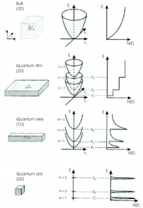
The nano-technology is dealing with the manipulation of materials in few atomic and molecular scale, where the constructed structure sized - at least in one dimension - is between one and one-hundred nanometer. This tech- nology allows to fabricate novel materials and electronic devices, where, the quantum mechanical eects (e.g. quantum connement) are very signicant.
The most conventional device fabrication is the so called top-down approach.
Here, smaller device is created from the larger material block with, material removal. These material removals should be dierent depending on the ob- ject. This removal can be mechanical like carving, milling, etching etc. In microelectronics, photolithography is a well known method to fabricate the required structure. In this technology, we can mark parts of the surface with a mask. We can also remove selectively parts from the thin lm or from the substrate material. This method is widely used in the silicon technol- ogy to fabricate devices like integrated circuits. Another fabrication method, which matches nano-technology, is the so called bottom-up approach. Here, we arrange large number of smaller components into very complex assem- blies, where the typical technology is epitaxial growth. We can grow in the bottom-up way quantum wells, quantum wires and quantum dots. Here, we exploit the self-organizing or self-assembling properties, which is - under special conditions - inherent to the materia. The self-assembly is a process,
11
where structures form without external inuence. This is the most typi- cal example of self-assembling system, from the physics of non-equilibrium processes, like the molecular epitaxial growth, detailed latter.
Bulk (3D)
Quantum film (2D)
Quantum wire (1D)
Quantum dot (0D)
N(E)
N(E)
N(E)
N(E)
E E
E E
E E
E E
2.1. Fig. The bulk and three dierent low-dimensional semiconductor struc- tures. Left part: The geometry; Middle part: The dispersion relation; Right part: Distribution of the density of states.
The quantum wells, quantum wires and quantum dots are two, one and zero dimensional structures, respectively. These low-dimensional structures have such properties, that carry novel possibilities in science and technology.
That way, we can fabricate entirely new electronic and optoelectronic de- vices. Quantum connement originate in structure, which conne electrons to regions comparable to their de Broglie wavelength. In free space, the electron can be move in all of the three directions of space. An unconned electron (can move x-, y-, z-directions) is described by the Schrödinger equa- tion. Where the solution of this equation is ϕk(r) = [1/(2π)3]eikr. Where k is the wavevector. The relative energy is as follows: E = h2k2/2m =
h2/2m(kx2+ky2+k2z).
The density state of a three-dimensional free electron gas calculated as follows g(E) = 1/2π2(2m/h2)3/2E1/2.
The diagram is shown in Fig. 2.1. When connement occurs in one direction in space, and the restriction on the motion of the electron is in the z-direction. then the free motion is possible only in x- or y-direction, when it is called two-dimensional (2D) structure or 2D electron gas. The energy of 2D electron gas is E =h2k2/2m =h2/2m(kx2+ky2)From this formula, the density state is constant, therefore independent of energy, g(E) =m/πh2.
This is the description of the strictly a 2D structure. The connement in z-direction tends to be zero. In practice, we regard a system quasi 2D, where the restriction is nite but small, (see Fig. 2.1). When the connement is in two directions (y and z), with the free motion in x-direction then the structure is one-dimensional (1D) structure or 1D electron gas. The energy of the 1D motion electron is given below E = h2k2/2m =h2/2m(k2x) Here, the expression of the density state from this calculation given as g(E) = 1/π(2m/h2)1/21/E1/2.
This density function in a quasi 1D case is shown in Fig. 2.1. When the connement is in x-, y-, and z-directions, the nit is a zero-dimensional (0D) electron gas. In this case we can neglect the interactions between electrons.
An ideal 0D electron is one that exists in a single state of xed energyE =E0. The density state is given by the Dirac delta-function g(E) = δ(E−E0).
A quasi 0D character is shown in Fig. 2.1. The realization of the described low-dimensional structures are detailed later [2, 3, 5, 8].
2.2. Material Scientic Background
2.2.1. Properties of the GaAs and Related Materials
In this section, the bulk properties of an articial material, namely the III-V compounds will be discussed. In the middle of the twenties century the semi- conducting properties of the III-V compounds was discovered by H. Welker [15, 35]. At that time it could not predicted, what a fruitful eld of semi- conductor physics and its practical application would be opened up by this discovery. The experimental results and the theoretical calculations show that the III-V compounds have similar semiconducting properties to that of germanium and silicon. The III-V compounds are formed from elements of
groups III and V of the periodic table. The rst investigated material was the InSb. It was impossible to imagine that these III-V materials would have very remarkable properties, e.g. extremely high electron mobility, more higher than the values observed at previously known semiconductors. Since then the major emphasis of the scientic investigations of the III-V compounds has shifted quickly into the device technology of these semiconductors.
Here, mostly the GaAs as a sample material of the III-V compounds will be treated. The III-V materials crystallize mostly in the so called zinc-blende structure. This structure is formed in the same way as the well know diamond lattice, except that the two nearest neighbor lattice point are occupied by dierent elements, as cation and anion. The structure is shown in the Fig.
2.2. The diamond and also the zinc-blende lattices can be considered as two interpenetrating face-centered cubic lattices. For the diamond lattice, such as germanium, all the atoms are the same. In the case of zinc-blende structure, e.g. GaAs, one sublattice is Ga and the other one is As. The two sublattices are oriented parallel to each other and are displaced from one another by quoter of the body diagonal of the elementary cube of the face-centered lattice (Fig. 2.2) [16, 17, 18, 29, 30, 31, 33, 34, 213].
2.2. Fig. The zinc-blende crystal structure for GaAs.
In the diamond and the zinc-blende lattices every atom is surrounded by its four nearest neighbors. In the case of the diamond lattice, the atoms have four valence electrons. The chemical bound between the nearest neighbor atom is formed by two valence electrons with opposite spin. In the case of zinc-blende lattices, the neighbors have unequal number of valence electrons,
but the sum of the valence electrons of two nearest neighbors is always eight.
Each atom, on the average, still has four valence electrons available for bound formation. It can be described quantum mechanically by sp3-hybrid wave functions. In the case of III-V materials, two kind of bonds can exist. Here, III-V compounds have primarily covalent bound, with only a small ionic bound contribution. In principle, the band structure of a solid is dened by the Schrödinger equation. In practice, because of the calculation diculties, suitable approximations and number crunching are required. The shape of the energy bands, the location of the band extrema within the Brillouin-zone is found in the literature [17, 35]. Most of the III-V compounds e.g. GaAs have direct band transition opposite to the elementary semiconductors e.g.
Si, which has indirect transition (Fig. 2.3).
2.3. Fig. Simple energy band structure for GaAs.
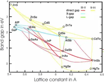
The III-V compounds are not only binary compounds, but they can also form ternary and quaternary compounds. With the change of the composi- tion, the band structure e.g. band gap changes as well. The function of the band gap v.s. lattice constant for the dierent III-V compounds are shown in Fig. 2.4.
It is important to talk about the phase diagram of these compounds [18, 19, 23, 24]. The basis of the ingot growth, the liquid phase epitaxy and also the droplet epitaxy is the control of the liquid-solid phase system. The phase diagram of the Ga-As system is described in Ref. [23, 25, 213, 28].
The phase rule states that the number of degrees of freedom in a system (f) is given by f = c− p+ 2, where c is the number of components and p is the number of phases. For a binary system e.g. GaAs, and pressure
BandgapineV
Lattice constant in A
2.4. Fig. Band gap versus lattice constant for dierent compound semicon- ductors.
variations are neglected, when c = 2, p = 2, then f = 1. In the case of ternary (quaternary) system c = 3 (or 4), and f = 2 (or 3). The phase diagram for a ternary (or quaternary) system are more complex than for a binary one. A simple model and its variants have been used sucessfully to interpolate existing ternary and quaternary phase diagram data. For further information, we refer to the literature [18, 23, 25, 22, 27].
These materials have very advantageous optical, charge carrier transport and other technological properties. The direct band gap made it possible to produce dierent optical devices such as light emitting diodes or laser diodes. The very high electron mobility make it possible to fabricate various high-ferquency devices in the microwave range. The special electronic struc- ture make it possible to produce a bulk device for microwave oscillator (Gunn diode). These materials can be produced by dierent epitaxial processes (liq- uid phase epitaxy (LPE), vapour phase epitaxy (VPE), and molecular beam epitaxy (MBE)). The properties of these materials allow us to grow layers and other structures with dierent composition on over each others. This property is so called homolog epitaxy. The lattice mismatch make it possible the production of the strain-induced nano-structures. The compound state give us the possibility for the droplet epitaxial method to produce dierent nano-structures (e.g. quantum dots (QDs) and rings (QRs)).
2.2.2. Surface Reconstruction of the III-V Materials
In this section we are dealing with the special structure of the surface, which is called surface reconstruction. The surface reconstruction means modied geometric and energy structure when compared to bulk properties. The ki- netics of the grown layer and other structure depends strongly on the surface reconstruction of the substrate. For our discussion, the sample material will be the GaAs, because, GaAs (001) has become the archetype for the study of reaction kinetics, growth mechanism of III-V compounds. The surface re- construction plays an important role in the homo- and heretoepitaxy to this family of materials [36, 38, 39, 40, 43, 91, 197].
[110]
2.5. Fig. Structure of (2x4) reconstruction for arsenic rich GaAs (001) sur- face. The dark circles represent As and the bright circles are Ga atoms.
The surface is always dierent from the bulk material, because it tries to relax by getting to an energy minimum state and involving various surface
reconstructions [36, 38, 39, 40, 41, 42, 197]. The atomic structure at the surface is much more complex than in the bulk material. The co-ordination number of the top most atoms is reduced. This means that a number of the so called dangling bonds are left unsaturated at the ideally terminated surface. In some crystallographic direction, like (001) and (111) the up and down sides are not the same. In contrast the (110) surface is non-polar and the atomic arrangement at the surface only involves relaxation. The (001) and (111) surfaces are terminated either by anions or by cations. These polar surfaces are electrostatically unstable. As a consequence, the atoms at the surface are rearranged to generate an electrostatic potential. This potential uctuates around zero with increasing distance into the crystal [43, 44]. The rearrangement of the surface atoms causes strain in the subsurface atomic layers closest to the surface, which are deformed. The reconstruction is not limited to the top most layer, thought the atomic displacements in the following layers are relatively small.
The reconstructions are also sensitive to temperature and the surface sto- ichiometry. These reconstructions can be understood since hybrid orbitals cannot form a bound at surfaces. Thus unreconstructed surfaces have un- saturated, that is partially lled dangling bonds, which are energetically unfavourable. The GaAs (001) surface can be terminated either As (see Fig.
2.5) or Ga atoms (see Fig. 2.27). We can observe two dangling bonds for each surface atom. In order to eliminate these dangling bonds, the surface undergoes complex reconstructions. In the case of the GaAs (001) surface, relative to the same surface of elemental semiconductors, the stoichiometry of the surface is especially signicant. Here the chemical composition strongly inuences the surface periodicity. In case of the stable surface, the dangling bonds of the electro-negative element (As) is occupied, and the dangling bonds of the electro-positive element (Ga) is empty [66, 269]. When these conditions is are satised, then the surface will be semiconducting, whereas partially lled dangling bonds may lead to a metallic surface.
The reconstructions depend on the surface stoichiometry. Technological, this means that the reconstructions are dependent on the substrate temper- ature and the ux of the components. The reconstructions have very compli- cated phase diagrams for each material and for dierent orientations of the surface. Rich variety of reconstructions are formed depending on surface stoi- chiometries. In rst approximation there are two reconstruction phases to be taken into account. The rst phase is when As rich surface forming at lower temperature, the second is when a surface, rich in Ga, forming at higher tem-
[110]
2.6. Fig. Structure of c(4x4) reconstruction for arsenic rich GaAs (001) sur- face. The dark circles represent As and the bright circles are Ga atoms.
perature. In case of GaAs the As rich formations are (2x4) (Fig. 2.5), c(2x8), c(4x4) (Fig. 2.6) or the Ga-rich are (4x2), c(8x2) (Fig. 2.7), (6x6), (4x6). Be- tween them there are transitory reconstructions such as (3x1), (1x6). Due to the symmetry, one particular reconstruction may represent dierent atomic arrangements. The exception is the case of the (2x4) reconstruction, where the well-established models have been questioned, and new structure model has been proposed, where the views of the c(4x4) surface are dierent. One author regards it Ga-rich and another as As-rich [38, 63, 258].
For growing GaAs, the most widely used kind of reconstruction is the β2(2x4), which in the direction of [¯110] forms lines, made up of As dimer pairs with trenches between them with depleted Ga. This surface is called As terminated, after this particular structure. During growth, this repre- sents a perfect surface with maximum reectivity, although the surface is
2.7. Fig. Structure of c(8x2) reconstruction for GaAs (001) surface. The dark circles represent As and the bright circles are Ga atoms.
obviously not at. For the Ga induced growth the starting surface is (2x4), formed in an As atmosphere [48, 91]. As the layers are grown one after the other, the surfaces of the successive layers become rougher, the oscillation decays and the specular spot intensity drops to minimum. In that case the Ga rich surface shows (4x2) reconstruction [48]. Tempering the surface, for reaching the maximum intensity, is carried out by heat-treatment in As rich atmosphere. With the increase of the secular spot intensity the (2x4) recon- struction reappeares again [36, 48, 91]. The various surface reconstructions are associated with dierent surface stoichiometry, which is closely linked to the RHEED intensity [63]. Although a large amount of information has already been compiled on the subject of surface reconstruction and its ef- fect on the intensity and growth, there are still no acceptable comprehensive explanation of the whole phenomenon.
2.3. Growth of Low-dimensional Structures
2.3.1. Some Aspects to the Growth Kinetics
In this section, we review the relevant microscopic processes taking place on the crystal surface. The morphology of the interface is determined by the interplay between deposition, desorption and surface diusion (Fig. 2.8).
2.8. Fig. Schematic illustration of several defects that may occur on a crystal surface.
The deposition, if an atom from the environment arrives at a random position on the surface, create bonds with the surface atoms, and sticks. An eect competing with deposition process is the desorption. During desorp- tion, some atoms deposited on the surface leave the interface. The probability of the desorption depends on how strongly the atom is bonded to the sur- face. When an atom is deposited on the surface, it forms bonds that must be broken before the desorption can occur. The strength of the bonds de- pends either on the type of atom or on the local geometry of the surface where the atom sticks. The lifetime of the deposited species is to measure the average time τ spent by this particle on the surface from deposition to desorption, which can be calculated with Arrhenius law τ =τ0exp(ED/kT). Where ED is the characteristic desorption energy. The desorption can be neglible for many materials under typical MBE conditions. The deposited atoms diuse on the crystal surface, searching for the energetically most fa- vorable position. The diusion length can be quite large, and depends on the temperature and the binding energies [72, 76, 77]. When a diusing atom meets an island where the interface height increases by one atom, it exhibits
a sticking preference for atoms located on the edge of the step. There is an additional potential barrier at the edge of the island that the atom must pass in order to jump o. This additional potential is called Erich-Schwöbel barrier [72, 76].
2.3.2. The Growth Modes
The structure growth can be classied in the following three modes: Layer- by-layer or Frank - van der Merve (FM), island or Volmer - Weber (VW) growth, and an intermediate mode (layer-plus-island) or Stranski - Krastanov (SK) mode (Fig. 2.9) [72, 76]. In the FM mode the interaction between the neighboring atoms in the layer is weaker than that with the substrate atoms. In the case of FM growth, islands of monolayer (ML) height coalesce before a new layer can nucleate on top of them. In the VW mode, the situation is opposite. In VW growth, growth proceeds to many atomic layers at discrete islands before these islands merge. In the SK mechanism, the growth is initiated in a layer-by-layer fashion, but islanding commences after the growth a certain thickness. In all but few situations, layer-by-layer growth is desirable because of the need for multilayered structures with at interfaces and smooth surfaces. This requires that the nucleation occur as a single even, on the substrate. In the case of SK, the lattice mismatch between the grown layer and the substrate material is the most common case. The deformation undergone by the even layer to match the lattice of the substrate. In this case, elastic energy is generated in the structure, which deforms mainly the lattice of the layer. When this deformation energy overcomes a critical value, it can be relaxed in two ways. One possible way is to nucleate nano-sized islands on the even layer, which layer is called as wetting layer. The absence of the lateral contains allow the atomic planes to laterally relax reducing the elastic energy in the structure. The another way is to introduce mist dislocations at the interface. According the rst mentioned way, so called strain-induced QD can be grown [197].
The nucleation is an important part of the growth. The nucleation can be understand with the help of the simple homogeneous nucleation process.
Homogeneous nucleation corresponds to direct condensation out of the gas phase, in absence of a substrate surface. This nucleation may proceed if a condition of supersaturation exists, meaning that the partial pressure of the nucleating species exceeds the equilibrium vapor pressure over the solid phase. Under a condition of supersaturation, embryos will form the vapor
VW SK FM .t
1t
22.9. Fig. Schematic illustration of the three growth modes. VW: Island growth or Vollmer - Weber growth mode; SK: Layer-plus-island growth or Stranski - Krastanov growth mode; FM: Layer-by-layer growth or Frank - van der Merve growth mode.
phase. Some embryos will grow by the inclusion of additional material from the vapor phase, if they are large enough so that their growth reduces the overall free energy of the system. Other embryos will be less than the critical embryo size and will shrink by reevaporation.
The heterogeneous nucleation is close to the nucleation in epitaxial and in heteroepitaxial growth. Heterogeneous nucleation takes place in the presence of a surface. This nucleation mode may be considered from macroscopic point view, in fashion paralleling the treatment of the homogeneous case.
The presence of a surface tends to increase the nucleation rate. This is because the nuclei may wet the substrate, greatly changing their geometry.
The epitaxial material will not wet the substrate, because this would be accompained by an overall increase in free energy of the system. The epitaxial deposit will spread out to maximize the area of the interface. For all other situations, consideration of partial wetting with a contact angle θ, where γs = γi +γecosθ.Where γe and γs represent the surface free energies of epitaxial crystal and substrate, respectively, and γi is the interfacial free energy. There are three types of situations: no wetting, partial wetting, and complete wetting. These situations correspons with FM, SK, and VW growth modes [76].
2.3.3. The Molecular Beam Epitaxy
The evaporation under ultra-high vacuum (UHV) is a classical method for preparing thin lm [70]. Depending on conditions, the deposited lms can also be crystalline. In this case the preparation method is called MBE [69, 71, 72, 73, 74, 75, 76, 77]. When the crystalline lm grows on a substrate dierent from that of the deposited material, so the process called heteroepitaxy. MBE technology is based on the controlled interaction of beams of atoms and molecules on a heated crystalline surface under UHV conditions. MBE is the most versatile method for preparing well dened surfaces, interfaces, layer structures and dierent nano-structures of elemental- (Si, Ge) and compound semiconductors (GaAs, InAs etc.). MBE method allows also growth of lm structures with sharp doping proles and dierent chemical composition (e.g.
AlGaAs) dierent lattice constant (e.g. GaAs/InGaAs junction). Multilayer structures with alternating doping or alternating band gap can be growth.
A new eld of band-gap-engineering was made possible by the development of MBE. Furthermore, QW, QD and other quantum structure can be grown with the help of MBE.
2.10. Fig. Scheme of a simplied UHV growth chamber for MBE.
As we mentioned before, MBE is a kind an UHV deposition technique, that involves the impingement of atomic or molecular beams onto a heated crystalline substrate where the epitaxially layer grow (Fig. 2.10). The source
of the molecular beams originate from eusion (Knudsen evaporation) cells (or gas-source crackers). These can be opened and closed very abruptly by shutters (or valves), providing atomic layer abruptness. Because MBE process takes place in a UHV environment, it is possible to employ a number of in-situ characterization tools based on electron (or ion) beams. These provide the crystal grower with immediate feedback, and improved control of the growth process. An MBE reactor chamber involves a number of source cells arranged radially in front of the substrate holder. The source cells supply all atoms necessary for the growth (and also for the doping) of the required semiconductor layers or of other nano-structures.
The mean free path for an evaporated atoms or molecule may be esti- mated if it assumed that all other particles in the system are at rest. If we suppose, that the evaporated particle is moving with velocity c, and all particles have around cross section with diameter σ. Two particles that pass at a distance of σ or less will collide. Therefore, each particle can be consid- ered to have a collosion cross section of πσ2, and the collosion volume swept out by a particle in time dt is πσ2cdt. If N is the volume concentration of particles then the collosion frequency will be f = Nπσ2cdt and the mean free path will be λ = c/f = (Nπσ2)−1. The free path can be calculated as a function of pressure: λ=kT /(√
2πσ2p). Typical value of the cross section diameter is about 2 Å, so the free path is about 103 cm at 10−5 Torr. This pressure represents the upper limit for the background pressure during the growth process. The requirement on the background pressure is considerably more stringent and is set by purity requirements. So, the base pressure to have about 10−10 Torr.
Dierent MBE variants have been developed. They are solid-source MBE (SS-MBE), gas-source MBE (GS-MBE), metalorganic MBE (MOMBE) etc.
The MBE chamber is equipped with pump system that give the above men- tioned base vacuum pressure in the range of10−10(or10−11) Torr. This UHV condition is required to reduce the back ground contaminant and it can be hinder the contamination of the deposited structure. (Because the UHV en- vironment quarantee the collosion-free path of the atoms and molecules from the source to the target.) GaAs and other related materials can be grown by MBE. These materials are most often grown on GaAs substrates (ori- ented mainly (001) direction). However, heteroepitaxy on Si, InP substrates has been investigated intensively with the goal of integrating AlGaAs de- vices with those from these other material systems. InGaAs is usually grown heteroepitaxially on InP or GaAs substrates.
2.3.4. The Jointed MBE Research Laboratory in the KFKI Campus
Our jointed MBE Research Laboratory of MFA and BMF (Legal successor today is ÓE.) was established in year 2008 [78, 79, 80]. The laboratory with the MBE equipment is located in Csillebérc, in KFKI Campus. Our MBE equipment is for growth of III-V compounds. The experimental setup described here is the only one presently in the whole country (Fig. 2.11).
2.11. Fig. View of our MBE equipment in the jointed laboratory.
This equipment consists of three UHV chambers. One of them is the reactor or main chamber for sample preparation. The main chamber has a heatable sample holder mounted on a precision manipulator. The sample is mounted on the Mo holder by liquid indium. In front of the sample holder, four Knudsen cells are located. Knudsen-type crucible are used as eusion cells for the evaporation. Our molecular sources are arsenic, Ga, In and Al.
These cells are tubular crucibles made from pyrolytic boron nitride. The crucibles are mounted within spiral Ta heater windings which are themselves enclosed within Ta-foil radiation shields. A requirement for the source oven and the whole unit is a very low production of impurities in the molecular beam. The oven set-up is therefore surrounded by a water cooled panel on which shutters are mounted which can close and open one or the other ef- fusion cell. Also the space between sources and the sample is shielded by a cooling shield at liquid nitrogen (see Fig. 2.13.). This chamber has also a 12 keV RHEED equipment (type Riber CER 606-ACE 1010) for monitoring of the sample during the growth (Fig. 2.12). A uorescent screen is located in opposite of the RHEED electron gun. Our MBE has a home made Fara- day cup to measure directly the electron current (the explanation see later).
A quadrupole mass spectrometer (QMS) (type: Pfeer QME 220) is also mounted on the chamber to investigate the environment during the growth process. The measuring range is to 300 amu. The vacuum can be measured also with a vacuum gauge.
Another chamber of the equipment is the loading chamber. This chamber has an two-axes manipulator with sample holder for places of ve samples, a load-lock window, an magnetic rod for the sample transport. This chamber is pumped by a turbo molecular pump (type: Pfeier HiPace 80). The pressure is measured by a vacuum gauge (type: Pfeier IKR 270). The third chamber is an additional chamber for vacuum pumps, they are a turbo molecular pump (type: Balzers TPU 520) and an iongetter pump (type: Varian Diode). Both pumps can be separated from the chamber with the help of gate valves (type:
VAT 160 CF). Further Vacuum valves are between the chambers.
The MBE growth needs very high requirements with the equipment. So we have to use a reliable and precise control [82, 123]. Before the crystal growing procedure started the equipment need to be heated up, following a specic temperature characteristics to evaporate dierent contaminating materials and clean the vacuum chamber (see Figure 2.13.). In our case, the UHV condition means 10−10 - 10−11 Torr pressure. After the closing of the system, we need the outheating of the chambers to achieve this vacuum level.
(A) (B)
2.12. Fig. Our equipment; (A) The view from the RHEED gun; (B) The view of the window of the load-loch chamber.
The outheating needs slow control without overshoot. The temperature is measured at 10 dierent points and around 10 heating wires are controlled.
The closed loop heat control is done by the Simatic S7 PLC which runs PI control algorithms to ensure error free tracking of the temperature setpoint [82, 84, 85].
For the sample preparation and its investigation, we need also very accu- rate control of the MBE equipment (Fig. 2.12). We have to control not only the heating out system of the vacuum chambers, but the control of the fur- nace of the molecular sources (Knudsen cells) and the control of the moving of the shutters. In the view-point of the electronics, the control is slow. The growth rate ranges between 0.1 - 1 ML/sec. In the case of the shutter move- ment, we need less slow control, because the shutter have to close before the next ML begin to growth. The heating of the eusion cells and the sample holder are also relatively slow processes because we need processes also free from overshoot. Because of the reliability, we use also PLC system for the
control of the MBE.
(F)
2.13. Fig. Some pictures about the MBE system during the installation. (A):
the main chamber with the electronics, (B): the additional chamber with the ion-getter pump, (C): inside of the reactor chamber, (D): the loading chamber, (E): the RHEED diagnostics (F): Heating control using PLC and OS.
The whole system is operated from a PC operator station (OS). The OS reads and writes the process variables of the PLC and, displays the system state (see Figure 2.13.). The temperature characteristics and other functions such as the sequential control of the molecular sources can be parameterized on the OS (and controlled by the PLC).
As we mentioned before, we use Faraday cup for intensity measurement of the electron beam. The RHEED pattern and oscillation intensities are
recorded usually by video camera focused on the uorescent screen. The uorescent lm on the window and the camera have non-linear behaviour in the intensity, which can deform the observed intensity distribution. If we want to investigate the real intensity and their accurate relation, we must measure the electron current directly. The direct measurement is possible by means of a Faraday cup. This cup has three pinholes along a line of decreasing diameters (0.5, 0.3, 0.1 mm) in order to obtain good angular resolution and suppression of the electron background. This cup is attached to an extra precision manipulator [86, 87].
2.4. In-situ Investigation of the Growth
2.4.1. Basic Concept of the RHEED
The RHEED is a widely used monitoring technique in the MBE growth [72, 77, 208]. This technique is applicable for surface structural analysis that is simple to implement, requiring only an electron gun and a uores- cent screen in the UHV chamber. RHEED has proved to be very versatile tool for growth and surface studies of semiconductor layer and other nano- structures prepared by MBE. The arrangement of MBE in which the atomic and molecular beams are incident ca. normally on the substrate plane enables diraction features to be monitored continuously during the growth process.
This investigation technique is based on the interaction of the electron beam and the studied surface, where beam energy is ranged typically between 1 - 3◦. The operation principle is illustrated in the Fig. 2.14.
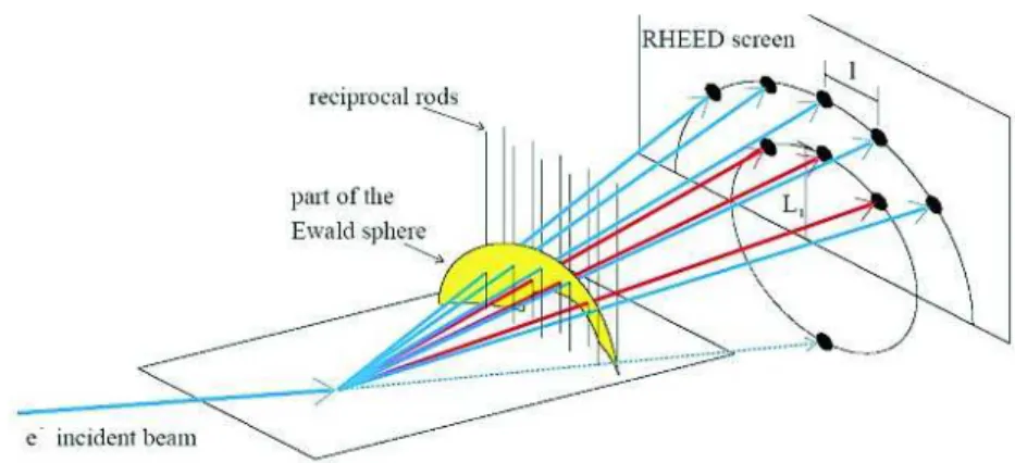
The incoming electrons with ¯k◦ wavevector have grazing incidence with respect to the surface plane. Therefore, they will mainly scattered from the top layer of the sample. The scattered wave vector of the electron beam k¯1 dier by a reciprocal-lattice vector of the surface G¯: k¯1 −k¯◦ = ¯G. When considering only elastic scattering, which means| ¯k1 |=| ¯k◦ | this diraction condition can be cast into geometrical construction of the Ewald sphere in reciprocal space. Where the arrow of ¯k◦ is attached to reciprocal-lattice point. The sphere around the origin of ¯k◦ with radius of | k¯◦ | denes the Ewald sphere. Reections can occur for all ¯k1 connecting the origin of this sphere and a reciprocal-lattice point on sphere (Fig. 2.14).
Because of its small penetration depth, owing to the interaction between the incident electron beam and surface atoms, RHEED is sensitive to the
2.14. Fig. Ewald sphere construction and diraction geometry of the RHEED.
atomic structure of the rst few planes. This technique is very appropriate to determine the surface reconstruction (Fig. 2.15). Diraction from a struture periodic in only two dimensions therefore underlines the observed patteren, and the positions of the elastically scattered beams can be determined from single scattering expression. The interpretation is very complicated and has many open questions, because of the unusually asymmetric scattering ge- ometry and of the necessity of accounting for multiple scattering processes [89, 90, 92].
2.15. Fig. The RHEED is very appropriate technique to determine the surface reconstruction. Demonstration of the (2x4) reconstruction.
On the uorescent screen, the intensity of the RHEED pattern changes during the crystal growth. Oscillatory response to a surface-sensitive probe during thin lm deposition is generally considered to be the manifestation of two dimensional layer-by-layer growth mode. This phenomenon can be explained as follows: At the beginning, the reection of the electron beam is high from the surface, resulting in high specular spot intensity. During the process of growth, crystalline islands forms on the surface. The initial surface loses its smoothness and becomes rougher. This results reduced reection, because of larger electron dispersion (Fig. 2.16). The model is a very rough simplication of the very complicated interaction [88, 90, 91, 93].
2.16. Fig. Lucid explanation of the RHEED oscillation originated by B. A.
Joyce.
The intensity of the specular beam depends on the incidence and the azimuth angle of the electron beam. The interaction on the surface can be treated as a multiple scattering process, so the elastic component of the
specular intensity is attributed mainly to multiple diraction and surface resonances. There is a very signicant contribution from inelastic and inco- herent processes, with the portion of elastic/inelastic process depending on azimuth, incidence angle and energy. As a result of the beam penetration it is also necessary to take account of refraction eects in considering the angular position of emergent electrons [88, 89, 90, 91, 92, 93].
2.4.2. Some Open Questions in the Interpretation of Static and Dynamic RHEED
As we mentioned before, the RHEED is a widely used monitoring technique during MBE growth. The orientation, quality and reconstruction of the grown surface can be determined by the RHEED pattern. Compared to other in-situ investigations, the glancing-incidence-angle geometry of RHEED is ideally for the in-situ observation of growth process and furthermore has very high surface sensitivity. The penetration depth of electron beam into the surface, can be changed by the variation of the incidence angle. The intensity of the RHEED pattern oscillates under appropriate conditions during the growth process [91]. One period of these oscillations corresponds exactly to the growth of one complete monolayer (ML) in the case of the layer-by-layer growth mode. The growth rate, and the composition in the case of alloy materials can be determined with the help of RHEED oscillations [48].
2.17. Fig. Intensity of RHEED specular spot as a function of the angle of [110] azimuth from GaAs (001) (2x4) reconstructed surface.
RHEED and its oscillations of intensity are very complex phenomena.
This technique is a versatile tool for in-situ monitoring, in spite of the fact that we do not know many details of its nature. This oscillation is characterized by the period, amplitude, phase and damping of the oscilla- tions, the behaviour at the initiation of growth, the recovery after growth and the frequency distribution in the Fourier spectrum of the oscillations.
The origin and describing of oscillation were investigated by several authors [38, 39, 41, 42, 197]. Many properties and behaviours of the oscillations are not yet understood. For example, some of these problems are the dierent phases of the specular and nonspecular RHEED beams [40], and the varied behaviour of the oscillations in the case of III-V and II-VI materials [41].
There are still more interesting and open problems in the topic of the decay of intensity oscillations and of the initial phase change, etc. Several authors have tried to describe these phenomena [42]. Several eects can be inter- preted by the above mentioned geometrical description. The oscillations in the case of two-dimensional growth mode, the disappearance of oscillations by step propagation, and the exponential decay of the oscillations can be explained by this geometrical description, too [42, 43, 44].
2.18. Fig. Phase relationship of RHEED specular spot as a function of the angle of [110] azimuth from GaAs (001) (2x4) reconstructed surface.
The RHEED is a suitable technique to investigate the binding properties on the surface. Furthermore, it is appropriate to distinguish special crys- tallographical directions, for which X-ray diraction (XRD) is unable. This crystallographical direction are e.g. on the (001) surface, where the [110] and
[1¯10] directions have dierent properties in crystallographical and in techno- logical view, too. However the dynamic RHEED is appropriate to determine and calibrate the growth parameters, such as e.g. growth rate and molecule ux [43, 44, 45]. One of the interesting problems is the initial phase change of the oscillation, which is depend on the direction of the incident electron beam, and the technological parameter, too.
The amplitude and period of the initial swing of RHEED oscillations are dierent from what follows. Except for the rst period, the measured decay of the oscillations ts well to an exponential function [43]. The incident electron beam impinges on the surface with low angle. If we change the incident or the azimuthal angle, the initial phase of the oscillations changes, too. For the phase change investigations, GaAs (001) serves as good model material [40, 42]. There are several models, which describe this phenomenon in broad range of incidence angle [45, 46]. These generally scattering based models take into account more MLs. These approaches describe qualitatively well the phase switch in the range of incident angle to about 4 but the tting e.g. at low angle under 2 has some deviation from the measured curve.
2.4.3. A Quantum Mechanical Interpretation of the RHEED Oscillation
A simple reection based model of the eect was described by Joyce soon af- ter the discovery of the oscillations [91]. According to his work, the oscillating intensity can be explained by the changing of the surface morphology. The complete layer which has maximum reection corresponds to the maximum intensity and the rough surface in intermediate state which has minimum reection corresponds to the minimum value of the oscillation respectively.
In this model the complete monolayer surface behaves as a perfect optical grating producing diraction pattern with the maximum possible contrast.
The building of the new layer manifests as more and more arising impurities that destroy the diraction pattern. As the growth process gets near to a perfect monolayer, at about half lled layer, where the diraction pattern has the least contrast, the holes, i.e., the spots without elements from the new layers start to be the impurities on the grating, thus with always de- creasing impurity number the diraction pattern starts to be regenerated.
The usefulness of this description can be underlined by the fact that it can be applied for the explanation of the intensity decay of RHEED oscillations
[48]. However, the symmetry to half-lled layer of the model and the asym- metry of the practical results are in contrast, thus more sophisticated models were introduced.
The diraction-like behaviour of the electron is used in the kinematical model introduced by Lent and Cohen, which can explain the origin of the RHEED intensity oscillations as well [102]. The particular oscillations are explained considering elastic and inelastic processes such as electron, phonon and plasmon scatterings on the surface layer as well as the rst few covered layers [103, 50].
These descriptions of the RHEED phenomenon are not fully satisfactory, i.e., they describe the behavior of the RHEED only under special conditions;
moreover, they contain rather rough approximations and neglections. The asymmetry of the oscillations to the half-lled layer is also not described. By introducing step density between the growing and the already grown layer, the model can be rened [105, 41, 107, 108], but the calculations become more complicated with more tting parameters.
However, we can not give up the semiquantitative quantum-mechanical approach. There is, e.g., the surface coherence length, which was introduced by Beeby [109], which was used for explaining the behaviour of the initial phase of RHEED oscillations [221], and which should be included in the further models of the reecting electrons.
The quantum-mechanically exact description of RHEED phenomenon is very sophisticated and practically it can not be carried out because of the high number of interacting particles. However, a phenomenological descrip- tion can be rather successful. The investigated quantum-mechanical entities, such as the electrons can be approximated as particles or waves under dif- ferent experimental conditions. The surface morphology is changed during the growth process, which causes changes in the experimental conditions.
These condition variations determine the type of the interaction. We usually say, that a quantum mechanical entity (like the electron) shows particle-like behavior if its path to the interaction place can be given exactly, i.e., in the case if we can somehow identify its path, there is only one energetically most ecient path. The same entity shows wave-like behavior if this path can not be exactly identied, i.e., it can move from one place to another along more dierent, but energetically indistinguishable paths. This complementary be- havior depends on the experimental conditions. The complementarity itself is independent of the uncertainty relation, which was demonstrated by Dürr, Nonn and Rempe in a two-slit experiment [111].
The observation of the path of a quantum entity is usually possible by its interactions with other quantum entities. Quantum entanglement of two or more quantum mechanical particles is generated during the interaction between these entities. According to the philosophy of Buchanan, these new quantum entanglements destroy the interference with any other entities, not entangled with the studied particle [112].
In our model philosophy, the quantum entanglement between the incom- ing electrons as quantum entities and the already present macroscopic dirac- tion lattice can be neglected. The electrons can however build correlated, or entangled states with the atoms or small clusters of atoms in the newly build- ing layer. (Similarly with the holes in the almost nished layers.) Usually, entanglement is meant between identical particles, but there is no strict rule against entanglement between electrons and more complex quantum mechan- ical objects. It is important to emphasize that the size of the investigated objects is small enough to exhibit quantum behavior. The quantum behav- ior of much larger objects (like C60 molecules) containing much more atoms was already shown [113]. The principle of complementarity and the quantum entanglement can help us in the description of RHEED oscillations.
2.19. Fig. The electron beam impinges on the sample under grazing incident angle. Upper part: Experimental arrangement at perfect surface. The elec- tron interacts with the crystal as a diraction lattice. Electron shows wave behavior. The quantum entanglement is insignicant in this case. Lower part: Experimental arrangement at rough surface. The electron interacts with atoms and atom groups. Electron shows particle behavior. The quan- tum entanglement is dominant in this case. ((a) and (b) mean intensity at perfect and imperfect surface, respectively.).
Let us investigate the RHEED phenomenon on the basis of above men-
tioned quantum mechanical ideas. If the crystal surface was complete and perfect, then the electron wave functions after the scattering on the complete
"grating" (the rows of the surface atoms) would dier in the phase. In the maximum intensity cases, the wave functions of the electrons sum up with their phase being the same, in dark point with exactly opposite phase, thus interference is obtained. To give a mathematical description, the wave func- tions with dierent phases are indexed with number 1, 2, 3, etc., thus the collective resulting function can be given as follows:
Ψ ∼Ψ1+ Ψ2+ Ψ3+. . . , (2.1) If the electron interacts with a perfect crystal surface, it behaves like a wave. The "electron wave" interacts with the crystal lattice as if it would be a diraction lattice. The size of the crystal is macroscopic. Experimentally reasonable quantum entanglement does not arise between the electron beam and the lattice. We can observe partial diraction pattern which originates from the interference of the electron waves. In these cases we do not have a denite path of the electron for the description of the interaction, i.e., we have several dierent paths simultaneously, because a translational crystal symmetry exists in the lateral direction of the surface. This experimental condition results in sharp diraction pattern as it is shown in the upper part of 2.19.
If the crystal surface is not fully occupied by atoms, the upper layer con- sists of quantum objects such as atoms, atom groups or holes in the layer.
These quantum objects are dierent although they consist of same atoms because they have dierent sizes, dierent shapes and dierent connections with the surface. These atoms and the atom groups are quantum objects with which the electron beam interacts quantum mechanically. The quantum en- tanglement generated by the incoming entities varies during the interaction.
The reason of this variation is, besides the topological dierence in the initial surface, the dierence in the growth process in dierent conditions. If the larger clusters of atoms (holes) are preferred during the growth process, the entanglement becomes less, while in case of small, but several clusters, the entanglement can be quite large, and can attain more incoming electrons.
For a mathematical summary of the entanglement, some notations should be introduced. Let us denote the dierent surface quantum objects with A, B, C, etc, the electrons with 1, 2, 3, etc. The resulting, entangled wave function can be given in a direct product wave function basis as
Ψ∼ |Ψ1i ⊗ |ΨAi+|Ψ2i ⊗ |ΨBi+|Ψ3i ⊗ |ΨCi+. . . , (2.2) where the numbered and lettered functions describe incoming electron and surface objects respectively. As the number of small clusters increases during the growth process, the number of possible quantum objects for in- teraction with the incoming electrons grows, thus formation of interfering substances has smaller probability. In this case the sharp diraction pattern is smoothened [112]. The electron interacts with the discrete entities on the surface, i.e., we can identify the electron path to the interaction place. The particle-like property of the electron dominates its behavior and overcomes the wave property. This results in a less intensive diraction as it is demon- strated in the lower part of 2.19. It can also happen, that the atom groups tend to cluster to larger, non quantum mechanical objects, and e.g. the holes in the newly growing layer tend to remain separated, in this case an inection, or even a turnback can arise in the contrast oscillation intensity plot.
2.20. Fig. Left part: The RHEED intensity distribution at smooth (solid line) and at rough (dashed line) surface. Right part: RHEDD intensity vs.
time; The intensity oscillation at the place of rod and background (b.g.) show opposite phase behavior. ((a) and (b) mean intensity at perfect and imperfect surface, respectively.).
According to these simple considerations the pattern intensity of the diraction has maximum value when the surface is perfect and at its min- imum value intensity takes place when the surface is roughest, i.e., when the largest number and most diuse interacting entities are present on the surface, thus the most of the entanglements can be formed. This state does
not always correspond to the half-lled layer in the growth process. The experimental results show that the background intensity between the dirac- tion rods has a small oscillation, too. The intensity oscillations of the peak and the background are in opposite phase [48]. Let us observe Fig. 2.20.
The intensity oscillations of the peak show a maximum value at smooth and minimum value at rough surface. Simultaneously, the oscillations of the background show exactly the opposite behavior, the maximum is when the surface is rough, and the minima take place at smooth surfaces.
2.4.4. Particular Behaviour of the RHEED
The phase of the oscillation depends on the incident angle of the electron beam. However the very useful kinematic theory does not predict the phase shift of the oscillations, which depends on the condition of the electron beam.
The contribution of inelastic processes such as Kikuchi scattering to the phase shift penomenon is not completely taken into account [91]. The RHEED phenomenon is partly reection-like and partly diraction-like. The eect of phase shift is described by the position of the minima of the oscillations. The behaviour of the minima and maxima of the oscillations can also be explained with a geometrical picture, which will be employed in this case. Because the specular spot is not a reected beam, the interaction of the electron beam and the target surface must be described quantum mechanically. The glancing- incidence-angle electron beam touches the surface over a large area. The reected-diracted information obtained does not come from the whole area.
The interaction between the surface and the electron beam exists only under special conditions, therefore we need to consider the surface coherence length (SCL) (w) [99]. The wave function after the interaction |Xai is written as follows:
|Xai=WB(r1)WT(r2)|χai, (2.3) where WB(r) and WT(r) are the wave packet of the electron beam and the interacting surface of the target, respectively. With the solution of this equation it can be shown that the SCL depends on the interaction potential between the incident electron and the target and depends less on the wave packet [109].
We can suppose that the SCL (w) is of the same order as the coherence length (Λ) of the beam. The energy of the electron beam is on the order of
2.21. Fig. The normalized touching length of the electron beam vs. incidence angle. The SCL is assumed to show similar behaviour.
E = 10 keV, with a de Broglie wavelength = 12.2×10⁻¹² m. The coherence length of the electron beam is [95]
Λ = λ
2βp
1 + (∆E+E)2 (2.4)
where 2β is the divergence of the electron beam and∆E is the full-width at half-maximum (FWHM) of the electron beam energy. These two quantities are usually 10−3 and 0.1 , respectively. The wave packet extends Λ1 = 12.2 nm with these values. The wave packet from interference investigations is 300λ [96]. By this measure we get Λ2 = 3.7 nm for the wave packet.
The spot size of the illuminating electron beam on the surface in the incident direction depends strongly on the incident angle. The size of the touching area between the beam and the surface in the case of unit beam width can be seen in Fig. 2.21. This dependence is very strong in the vicinity of an incident angle of 1◦. We can suppose that the SCL depends on the incident angle, too.
The relation between the size of characteristic growth terrace (s) and the SCL (w) in the case of a polycrystalline surface was investigated in Ref [109]. This concept can be applied in our case if we use, instead of domains, identically oriented growth units (or growth terraces).
An estimate of the characteristic dimension of a growth terrace can be
given from experiments. The terrace average width (s) and the migration length of Ga (l) depend on the substrate temperature. The RHEED oscil- lations are present if l ≤ s and absent if l ≥ s. In our case, the migration length is 7 nm because the substrate temperature is 580 ◦C [91].
2.22. Fig. The lattice of GaAs projected on the (001) plane. The red and green circles represent the As and Ga atoms, respectively. The black tri- angles are the dangling bonds, which cause dierent rates of composition (growth) and decomposition (etching) of the crystal in dierent directions.
The component of growth rate in the direction of the investigating electron beam rk and the perpendicular components r⊥.
The binding energy on the (001) surface in the direction [110] and [1¯10] is not the same, which explains the dangling bonds in Fig. 2.22. This anisotropy is manifested in the dierent growth rates. The growth rate in the [110] direction is larger than that in the perpendicular direction [97]. This anisotropy is apparent not only in the growth of the crystal (in other words composition of the crystal) but also in the etching (that is decomposition) of the crystal. The growth rates in the [110] and [1¯10] directions are dierent by more than factor of two. This factor can be estimated with the help of etch-pit shapes [98].
We can suppose that the SCL and the average terrace width have com- mensurate dimensions at glancing-incidence-angles (w ≈ s). This supposi- tion seems right, because the touching length of the electron beam (also the SCL after our supposition) changes very abruptly at angles less than 1◦ and in this region the function t3/2/T is constant accordingly as w > s. The