Table 14-0.
Listing 14-0.
Overview
This chapter describes the basic system interface features of the
ADSP-2191 family processors. The system interface includes various hard- ware and software features used to control the DSP processor.
Processor control pins include a RESET signal, clock signals, flag inputs and outputs, and interrupt requests. This chapter describes only the logical relationships of control signals; see the ADSP-2191 DSP Microcomputer Datasheet for actual timing specifications.
Pin Descriptions
This section provides functional descriptions of the ADSP-2191 processor pins. Refer to the data sheet for the ADSP-2191 for more information, including pin numbers for the 144-Lead LQFP and the 144-Lead Mini-BGA packages.
ADSP-2191 pin definitions are listed in Table 14-1 on page 14-2. All of the ADSP-2191 pins are asynchronous.
Unused inputs should be tied or pulled to VDDEXT or GND, except for
ADDR21–0, DATA15–0, PF7-0, and inputs that have internal pull-up or pull-down resistors (TRST, BMODE0, BMODE1, OPMODE, BYPASS, TCK, TMS, TDI, and RESET); these pins can be left floating. These pins have a logic-level hold circuit that prevents them from floating internally.
Pin Descriptions
The following symbols appear in the Type column of Table 14-1:
G = Ground, I = Input, O = Output, P = Power Supply, and T = Three-State.
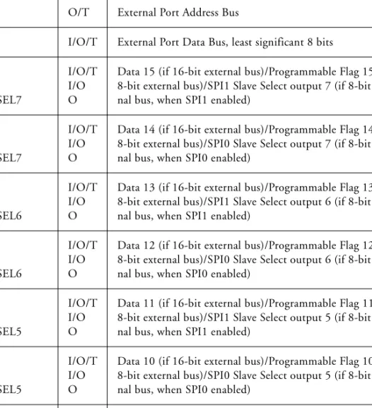
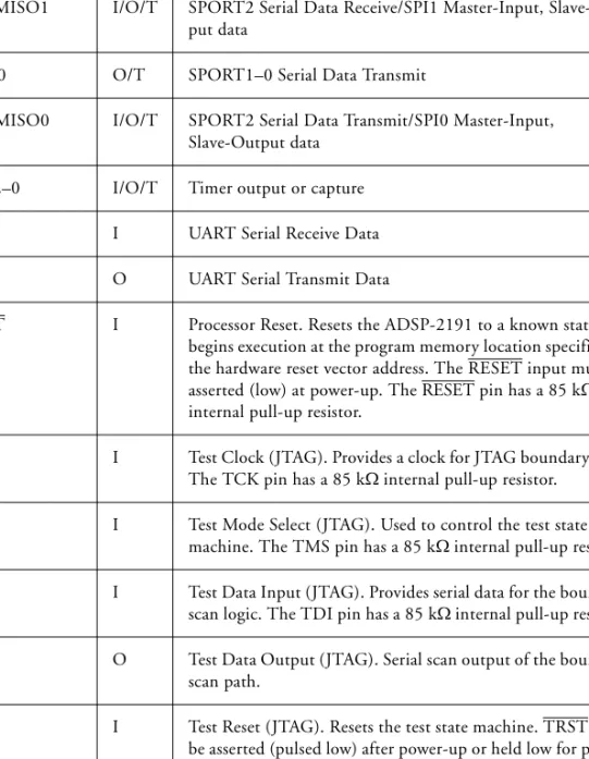
Table 14-1. Pin Descriptions
Pin Type Description
A21–0 O/T External Port Address Bus
D7–0 I/O/T External Port Data Bus, least significant 8 bits D15
/PF15 /SPI1SEL7
I/O/T I/O O
Data 15 (if 16-bit external bus)/Programmable Flag 15 (if 8-bit external bus)/SPI1 Slave Select output 7 (if 8-bit exter- nal bus, when SPI1 enabled)
D14 /PF14 /SPI0SEL7
I/O/T I/O O
Data 14 (if 16-bit external bus)/Programmable Flag 14 (if 8-bit external bus)/SPI0 Slave Select output 7 (if 8-bit exter- nal bus, when SPI0 enabled)
D13 /PF13 /SPI1SEL6
I/O/T I/O O
Data 13 (if 16-bit external bus)/Programmable Flag 13 (if 8-bit external bus)/SPI1 Slave Select output 6 (if 8-bit exter- nal bus, when SPI1 enabled)
D12 /PF12 /SPI0SEL6
I/O/T I/O O
Data 12 (if 16-bit external bus)/Programmable Flag 12 (if 8-bit external bus)/SPI0 Slave Select output 6 (if 8-bit exter- nal bus, when SPI0 enabled)
D11 /PF11 /SPI1SEL5
I/O/T I/O O
Data 11 (if 16-bit external bus)/Programmable Flag 11 (if 8-bit external bus)/SPI1 Slave Select output 5 (if 8-bit exter- nal bus, when SPI1 enabled)
D10 /PF10 /SPI0SEL5
I/O/T I/O O
Data 10 (if 16-bit external bus)/Programmable Flag 10 (if 8-bit external bus)/SPI0 Slave Select output 5 (if 8-bit exter- nal bus, when SPI0 enabled)
D9 /PF9 /SPI1SEL4
I/O/T I/O O
Data 9 (if 16-bit external bus)/Programmable Flag 9 (if 8-bit external bus)/SPI1 Slave Select output 4 (if 8-bit external bus, when SPI1 enabled)
D8 /PF8 /SPI0SEL4
I/O/T I/O O
Data 8 (if 16-bit external bus)/Programmable Flag 8 (if 8-bit external bus)/SPI0 Slave Select output 4 (if 8-bit external bus, when SPI0 enabled)
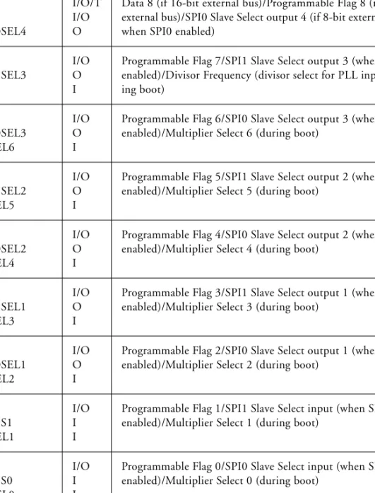
PF7 /SPI1SEL3 /DF
I/O O I
Programmable Flag 7/SPI1 Slave Select output 3 (when SPI0 enabled)/Divisor Frequency (divisor select for PLL input dur- ing boot)
PF6 /SPI0SEL3 /MSEL6
I/O O I
Programmable Flag 6/SPI0 Slave Select output 3 (when SPI0 enabled)/Multiplier Select 6 (during boot)
PF5 /SPI1SEL2 /MSEL5
I/O O I
Programmable Flag 5/SPI1 Slave Select output 2 (when SPI0 enabled)/Multiplier Select 5 (during boot)
PF4 /SPI0SEL2 /MSEL4
I/O O I
Programmable Flag 4/SPI0 Slave Select output 2 (when SPI0 enabled)/Multiplier Select 4 (during boot)
PF3 /SPI1SEL1 /MSEL3
I/O O I
Programmable Flag 3/SPI1 Slave Select output 1 (when SPI0 enabled)/Multiplier Select 3 (during boot)
PF2 /SPI0SEL1 /MSEL2
I/O O I
Programmable Flag 2/SPI0 Slave Select output 1 (when SPI0 enabled)/Multiplier Select 2 (during boot)
PF1 /SPISS1 /MSEL1
I/O I I
Programmable Flag 1/SPI1 Slave Select input (when SPI1 enabled)/Multiplier Select 1 (during boot)
PF0 /SPISS0 /MSEL0
I/O I I
Programmable Flag 0/SPI0 Slave Select input (when SPI0 enabled)/Multiplier Select 0 (during boot)
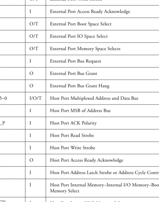
RD O/T External Port Read Strobe
Table 14-1. Pin Descriptions (Cont’d)
Pin Type Description
Pin Descriptions
WR O/T External Port Write Strobe
ACK I External Port Access Ready Acknowledge BMS O/T External Port Boot Space Select
IOMS O/T External Port IO Space Select MS3–0 O/T External Port Memory Space Selects
BR I External Port Bus Request
BG O External Port Bus Grant
BGH O External Port Bus Grant Hang
HAD15–0 I/O/T Host Port Multiplexed Address and Data Bus HA16 I Host Port MSB of Address Bus
HACK_P I Host Port ACK Polarity
HRD I Host Port Read Strobe
HWR I Host Port Write Strobe
HACK O Host Port Access Ready Acknowledge
HALE I Host Port Address Latch Strobe or Address Cycle Control HCMS I Host Port Internal Memory–Internal I/O Memory–Boot
Memory Select
HCIOMS I Host Port Internal I/O Memory Select CLKIN I Clock Input/Oscillator input 0
Table 14-1. Pin Descriptions (Cont’d)
Pin Type Description
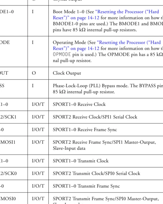
XTAL O Crystal output
BMODE1–0 I Boot Mode 1–0 (See “Resetting the Processor (“Hard Reset”)” on page 14-12 for more information on how the BMODE1-0 pins are used.) The BMODE1 and BMODE0 pins have 85 kΩ internal pull-up resistors.
OPMODE I Operating Mode (See “Resetting the Processor (“Hard Reset”)” on page 14-12 for more information on how the OPMODE pin is used.) The OPMODE pin has a 85 kΩ inter- nal pull-up resistor.
CLKOUT O Clock Output
BYPASS I Phase-Lock-Loop (PLL) Bypass mode. The BYPASS pin has a 85 kΩ internal pull-up resistor.
RCLK1–0 I/O/T SPORT1–0 Receive Clock
RCLK2/SCK1 I/O/T SPORT2 Receive Clock/SPI1 Serial Clock RFS1–0 I/O/T SPORT1–0 Receive Frame Sync
RFS2/MOSI1 I/O/T SPORT2 Receive Frame Sync/SPI1 Master-Output, Slave-Input data
TCLK1–0 I/O/T SPORT1–0 Transmit Clock
TCLK2/SCK0 I/O/T SPORT2 Transmit Clock/SPI0 Serial Clock TFS1–0 I/O/T SPORT1–0 Transmit Frame Sync
TFS2/MOSI0 I/O/T SPORT2 Transmit Frame Sync/SPI0 Master-Output, Slave-Input data
DR1–0 I/T SPORT1–0 Serial Data Receive
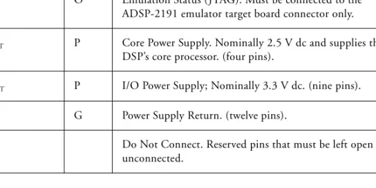
Table 14-1. Pin Descriptions (Cont’d)
Pin Type Description
Pin Descriptions
DR2/MISO1 I/O/T SPORT2 Serial Data Receive/SPI1 Master-Input, Slave-Out- put data
DT1–0 O/T SPORT1–0 Serial Data Transmit
DT2/MISO0 I/O/T SPORT2 Serial Data Transmit/SPI0 Master-Input, Slave-Output data
TMR2–0 I/O/T Timer output or capture
RXD I UART Serial Receive Data
TXD O UART Serial Transmit Data
RESET I Processor Reset. Resets the ADSP-2191 to a known state and begins execution at the program memory location specified by the hardware reset vector address. The RESET input must be asserted (low) at power-up. The RESET pin has a 85 kΩ internal pull-up resistor.
TCK I Test Clock (JTAG). Provides a clock for JTAG boundary scan.
The TCK pin has a 85 kΩ internal pull-up resistor.
TMS I Test Mode Select (JTAG). Used to control the test state machine. The TMS pin has a 85 kΩ internal pull-up resistor.
TDI I Test Data Input (JTAG). Provides serial data for the boundary scan logic. The TDI pin has a 85 kΩ internal pull-up resistor.
TDO O Test Data Output (JTAG). Serial scan output of the boundary scan path.
TRST I Test Reset (JTAG). Resets the test state machine. TRST must be asserted (pulsed low) after power-up or held low for proper operation of the ADSP-2191. The TRST pin has a 65 kΩ internal pull-down resistor.
Table 14-1. Pin Descriptions (Cont’d)
Pin Type Description
Recommendations for Unused Pins
The following is a list of recommendations for unused pins.
• If the CLKOUT pin is not used, turn it OFF, by clearing bit 6 (CKOUTEN) of the PLL control register.
• If the Interrupt/Programmable Flag pins are not used, configure them as inputs at reset and function as interrupts and input flag pins, pull the pins to an inactive state, based on the POLARITY setting of the flag pin.
• If a flag pin is not used, configure it as an output. If for some reason, it cannot be configured as an output, configure it as an input. Use a 100 kΩ pull-up resistor to VDD (or, if this is not possible, use a 100 kΩ pull-down resistor to GND).
• If a SPORT is not used completely and if the SPORT pins do not have a second functionality, disable the SPORT and let the pins float.
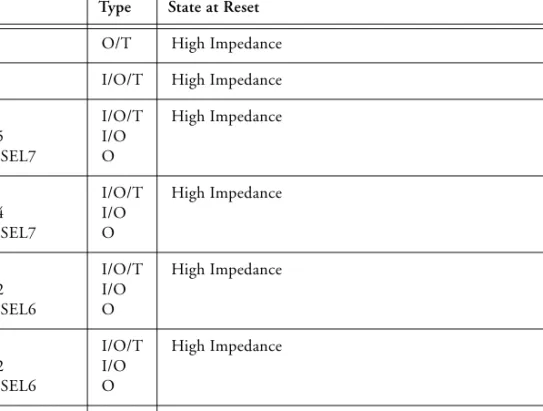
EMU O Emulation Status (JTAG). Must be connected to the ADSP-2191 emulator target board connector only.
VDDINT P Core Power Supply. Nominally 2.5 V dc and supplies the DSP’s core processor. (four pins).
VDDEXT P I/O Power Supply; Nominally 3.3 V dc. (nine pins).
GND G Power Supply Return. (twelve pins).
NC Do Not Connect. Reserved pins that must be left open and unconnected.
Table 14-1. Pin Descriptions (Cont’d)
Pin Type Description
Pin States at Reset
• If the receiver on a SPORT is the only part being used, use resistors on the other pins. However, if the other pins are outputs, let them float.
Pin States at Reset
The following table shows the state of each pin during and after reset. See
“Pin Descriptions” on page 14-1 for a description of each of these pins.
The following symbols appear in the Type column of Table 14-2:
G = Ground, I = Input, O = Output, P = Power Supply, and T = Three-State.
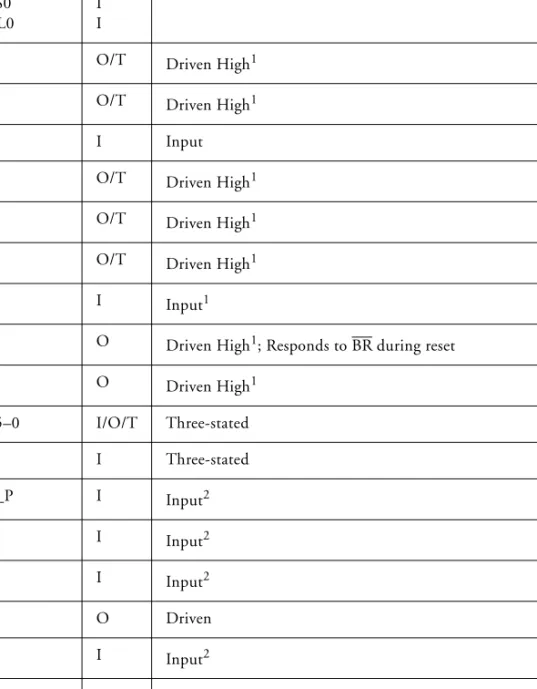
Table 14-2. Pin States at Reset
Pin Type State at Reset
A21–0 O/T High Impedance
D7–0 I/O/T High Impedance
D15 /PF15 /SPI1SEL7
I/O/T I/O O
High Impedance
D14 /PF14 /SPI0SEL7
I/O/T I/O O
High Impedance
D13 /PF12 /SPI1SEL6
I/O/T I/O O
High Impedance
D12 /PF12 /SPI0SEL6
I/O/T I/O O
High Impedance
D11 /PF11 /SPI1SEL5
I/O/T I/O O
High Impedance
D10 /PF10 /SPI0SEL5
I/O/T I/O O
High Impedance
D9 /PF9 /SPI1SEL4
I/O/T I/O O
High Impedance
D8 /PF8 /SPI0SEL4
I/O/T I/O O
High Impedance
PF7 /SPI1SEL3 /DF
I/O O I
Input
PF6 /SPI0SEL3 /MSEL6
I/O O I
Input
PF5 /SPI1SEL2 /MSEL5
I/O O I
Input
PF4 /SPI0SEL2 /MSEL4
I/O O I
Input
PF3 /SPI1SEL1 /MSEL3
I/O O I
Input
PF2 /SPI0SEL1 /MSEL2
I/O O I
Input
PF1 /SPISS1 /MSEL1
I/O I I
Input
Table 14-2. Pin States at Reset (Cont’d)
Pin Type State at Reset
Pin States at Reset
PF0 /SPISS0 /MSEL0
I/O I I
Input
RD O/T Driven High1
WR O/T Driven High1
ACK I Input
BMS O/T Driven High1
IOMS O/T Driven High1
MS3–0 O/T Driven High1
BR I Input1
BG O Driven High1; Responds to BR during reset
BGH O Driven High1
HAD15–0 I/O/T Three-stated
HA16 I Three-stated
HACK_P I Input2
HRD I Input2
HWR I Input2
HACK O Driven
HALE I Input2
HCMS I Input2
HCIOMS I Input2
Table 14-2. Pin States at Reset (Cont’d)
Pin Type State at Reset
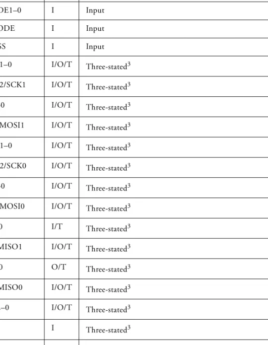
CLKIN I Input
BMODE1–0 I Input
OPMODE I Input
BYPASS I Input
RCLK1–0 I/O/T Three-stated3 RCLK2/SCK1 I/O/T Three-stated3 RFS1–0 I/O/T Three-stated3 RFS2/MOSI1 I/O/T Three-stated3 TCLK1–0 I/O/T Three-stated3 TCLK2/SCK0 I/O/T Three-stated3 TFS1–0 I/O/T Three-stated3 TFS2/MOSI0 I/O/T Three-stated3
DR1–0 I/T Three-stated3
DR2/MISO1 I/O/T Three-stated3
DT1–0 O/T Three-stated3
DT2/MISO0 I/O/T Three-stated3 TMR2–0 I/O/T Three-stated3
RXD I Three-stated3
TXD O Three-stated3
RESET I Input2
Table 14-2. Pin States at Reset (Cont’d)
Pin Type State at Reset
Resetting the Processor (“Hard Reset”)
Resetting the Processor (“Hard Reset”)
The RESET signal halts execution and causes a hardware reset of the proces- sor; the program control jumps to address 0xFF0000 and begins execution of the boot ROM code at that location. (If configured in “no boot” mode, the DSP begins execution from PM 0x10000.)
TCK I Input4
TMS I Input4
TDI I Input4
TDO O Three-stated4
TRST I Input4 (pulled low by resistor)
EMU O Three-stated4 ((open drain with internal pullup) NC
1 Three-stated when the DSP is bus slave (held in BR).
2 Bus Master independent.
3 SPI, SPORT, UART.
4 JTAG.
Table 14-2. Pin States at Reset (Cont’d)
Pin Type State at Reset
The ADSP-2191 can be booted via the EPROM, UART, SPI, or Host port. The DSP looks at the values of three pins (BMODE0, BMODE1, and
OPMODE) to determine the boot mode, as shown in the following table.
After the DSP has determined the boot mode, it loads the headers and data blocks. For some booting modes, the boot process uses DMA. For more information about DMA, see “I/O Processor” on page 6-1.
The RESET signal must be asserted (held low) when the processor is pow- ered up to assure proper initialization.
The internal clock on the ADSP-2191 requires approximately 500 clock cycles to stabilize. To maximize the speed of recovery from reset, CLKIN should run during the reset.The power-up sequence is defined as the total time required for the crystal oscillator circuit to stabilize after a valid VDD is applied to the processor and Table 14-3. Hard Reset Boot Mode Pins
OPMODE BMODE1 BMODE0 Result
0 0 0 No boot; run from external 16-bit memory starting at address 0x10000
0 0 1 Boot from EPROM
0 1 0 Boot from Host
0 1 1 Reserved
1 0 0 No boot; run from external 8-bit memory, bypass ROM, starting at address 0x10000
1 0 1 Boot from UART
1 1 0 Boot from SPI, up to 4K bits
1 1 1 Boot from SPI, >4K bits up to 512K bits
Resetting the Processor (“Hard Reset”)
for the internal PLL to lock onto the specific crystal frequency. A mini- mum of 500 CLKIN cycles ensures that the PLL has locked, but it does not include the crystal oscillator start-up time. During the power-up sequence the RESET signal should be held low.
If a clock has not been supplied during RESET, the processor does not know it has been reset and the registers won’t be initialized to the proper values.At powerup, if RESET is held low (asserted) without any input clock signal, the states of the internal transistors are unknown and uncon- trolled. This condition could lead to processor damage.
“ADSP-219x DSP Core Registers” on page A-1 and “ADSP-2191 DSP I/O Registers” on page B-1 contain tables showing the RESET states of var- ious registers, including the processors’ on-chip memory-mapped
status/control registers. The values of any registers not listed are undefined at reset. The contents of on-chip memory are unchanged after RESET, except as shown in the tables for the I/O memory-mapped control/status registers. The CLKOUT signal continues to be generated by the processor during RESET, except when disabled.
When in Clock Multiplier mode (not Bypass mode), the MSELx pins, which define the clock multiplier ratios, are sampled during reset.For information on managing these pins, see “Managing DSP Clocks” on page 14-32.
The contents of the computation unit (ALU, MAC, Shifter) and data address generator (DAG1, DAG2) registers are undefined following RESET. When RESET is released, the processor’s booting operation takes place, depending on the states of the processor’s BMODEx and OPMODE pins. (Pro- gram booting is described in “Boot Mode DMA Transfers” on page 6-32.)
When the power supply and clock remain valid, the content of the on-chip memory is not changed by a software reset.Resetting the Processor (“Soft Reset”)
A software reset is generated by writing ones to the Software Reset (SWR) bits in the Software Control register. Note that a software reset affects only the state of the core and the peripherals (as defined by the peripheral registers documented in“ADSP-2191 DSP I/O Registers” on page B-1).
During a soft reset, the DSP does not sample the boot mode pins, rather it gets its boot information from the Next System Configuration (NXTSCR) register.
If the—No Boot on Software Reset—Run mode (RMODE) bit of the Next System Configuration Register has been set to 0, following a soft reset, program flow jumps to address 0xFF0000 and begins executing the boot ROM code at that location to reboot the DSP. A software reset can also be used to reset the boot mode without doing an actual reboot. If bit 4 of the Next System Configuration Register has been set to 1, following a soft reset, program flow jumps to address 0x000000 and completes reset with- out rebooting the DSP.
The ADSP-2191 can be booted via the EPROM, UART, SPI, or Host port. The DSP uses three bits of the System Configuration (SYSCR) register (loaded from NXTSCR on soft reset) to determine the boot mode, as shown in Figure B-2 on page B-18. (Note that these three bits correspond to the
BMODE0, BMODE1, and OPMODE pins used to determine the boot mode for a hard reset, as described in “Resetting the Processor (“Hard Reset”)” on page 14-12.)
“ADSP-219x DSP Core Registers” on page A-1 and “ADSP-2191 DSP I/O Registers” on page B-1 contain tables showing the state of the proces- sor registers after a software reset that includes a DSP reboot. The values of any registers not listed are unchanged by a reboot.
The MSELx pins are not sampled during a software reset.Booting the Processor (“Boot Loading”)
Because the ADSP-2191’s shadow write FIFO automatically pushes the write to internal memory as soon as the write does not compete with a read, this FIFO’s operation is completely transparent to pro- grams, except in software reset/restart situations. To ensure correct operation after a software reset, software must perform two“dummy” writes to memory before writing the software reset bit.
For more information, see “Shadow Write FIFO” on page 5-15.
Booting the Processor (“Boot Loading”)
The ADSP-2191 has a booting scheme that is different from previous Analog Devices fixed-point DSP’s, such as the ADSP-218x. When the ADSP-218x comes out of reset, it is configured to automatically boot in a
“Loader Kernel” using DMA. This Loader Kernel then loads in corre- sponding “page loaders”. On the ADSP-2191, the boot Kernel is located on-chip and stored in a 24-bit wide, 1K ROM. The starting address of this boot ROM begins at 0xFF0000 (i.e., the first location of page 255).
For more information on the ADSP-2191 memory map, see Figure 5-3 on page 5-9.
Whether the DSP is reset with hardware (RESET pin) or software (SWR bits in the SWRST register), the boot kernel executes its process. For more infor- mation on reset, see “Resetting the Processor (“Hard Reset”)” on
page 14-12 and “Resetting the Processor (“Soft Reset”)” on page 14-15.
Boot Modes
Figure 14-1 shows the program flow for the boot kernel. Following a reset, the first operation performed by the boot Kernel is to read the Reset Configuration Register and determine the DSP boot mode.
In the event that the DSP is configured to boot from a peripheral, the first operation performed by the boot Kernel is to read in the first word of the bootstream. This control word contains information on the rest of the
Figure 14-1. Boot Process Flow
~RESET de-asserted: Program control jumps to memory address 0xFF0000, the first location of
the BOOT ROM kernel
Host Boot? No Boot?
(Execute from 8-bit or 16-bit
EMI)
Jump to first location of external memory (0x10000) to begin execution Configure External Memory Interface per system requirements EPROM Boot?
SPI Boot?
Auto-baud routine UART Boot?
BOOT ROM routine reads RESET Configuration Register to determine method of
booting based on MODE pins
Read “Control” word of Boot stream to determine 8- or 16-bit EPROM, wait
states information Set-up loop to poll
Semaphore A register, waiting for Host Processor to write it
Jump to first location of internal memory (0x00000) to begin execution
Read Control Word
Read Control Word
Final setup and LJUMP to 0x000000
Setup Direct Reads to load
data Block
Final DM Read?
Setup Direct Reads to load
data Block
Set up routine to read in first header
Parse header Initialize
Accordingly
Setup DMA to load data
block
No Set up DMA
to load header
Parse header Initialize Accordingly
Block larger than 32
words?
Final Yes DM?
No
Zero_PM or Zero_DM?
Yes
Yes No
Final DM?
No Zero_PM or
Zero_DM?
Yes
Yes
No
Once DMA is complete, set up
next header
Yes No
Booting the Processor (“Boot Loading”)
boot. The DSP performs this transfer using the modes that the DSP is configure with at reset (e.g., 8-bit external to 16-bit internal packing mode in case of the external memory interface, with maximum wait states and base clock divisor).
If it is determined that the DSP is not going to boot in a program, but instead run a program from 8-bit or 16-bit external memory, the boot ROM routine sets up the External Memory Interface and the External Access Bridge register for the desired packing mode (8-bit external to 24-bit internal or 16-bit-external-to-24-bit internal). Then, execution jumps to the first location of external memory (0x10000), where the user program is executed.
SPI Port and UART Port Booting
If booting via a peripheral such as the SPI or UART, the Loader Kernel will set up the corresponding peripheral as follows:
• SPI: SPI0 is used, set up as master, and is set to receive 8-bit words received MS-Bit first, SCLK = peripheral clock/60, with an
active-low serial clock to be compatible with commonly available serial EEPROMS.
• UART: In the case of UART boot, the Loader Kernel begins by first running an Auto-baud routine using a timer to determine the baud-rate of the external UART device. Once the baud-rate has been determined, the Loader Kernel will proceed with the rest of boot.
If booting via the SPI or UART, the corresponding DMA engines associ- ated with the peripheral are not used at all, but rather all the data is read in through core reads a byte at a time and packed internally by the Boot Kernel.
The external device transmits the word “0xaa” to allow the timer to cap- ture the pulse width of the device. Once the baud rate has been
determined, the DSP UART will transmit the words 0x4F and 0x4B cor- responding to “OK” in ASCII. The external device can now begin transmitting the boot file.
Host Port Booting
If booting via a Host processor, the Loader Kernel will relocate the Inter- rupt vector location to page 0 of memory. It will then sit in a loop polling the Semaphore A register (IO:0x1CFC), waiting for a Host Processor to write to it. The Host processor has the responsibility of loading the code and data into the DSP.
The ADSP-2191 can be booted from either an 8-bit, 16-bit, or 32-bit Host processor. In the case of booting from a 32-bit Host, the Host must send data on the 16 least significant data lines (right-justified).
The Host boot is configured to always use little-endian format, as this is the default that the Host port comes up in.
Example: If the representation of decimal number 1025 is 00000100 00000001, the Table 14-4 describes big and little endian representation of the number.
Table 14-4. Big and Little Endian Comparison
Address Big-Endian
Representation of 1025
Little-Endian Representation of 1025
00 - 00000001
01 - 00000100
02 00000100 -
03 00000001 -
Booting the Processor (“Boot Loading”)
After the Host processor has finished loading the ADSP-2191, it indicates this by writing a “1” to the Semaphore A Register (IO:0x1CFC). The Boot Kernel will then exit the polling loop and transfers program control to the first location of page 0.
External Memory Interface Booting
If booting via the EMI, the Loader Kernel sets up the corresponding sys- tem and control registers and the wait state control register accordingly.
The Kernel will then set up a DMA transfer block to read in the first header of the bootstream via DMA.
For BMS to MSx boot sequences, the EMI bus widths must match.The DSP cannot boot 8-bit MSx space from a 16-bit BMS. Also, the DSP cannot boot 16-bit MSx space from an 8-bit BMS.
After a header is read in, the Loader Kernel will parse the header and set up another DMA transfer block to load in the actual data following this header. While this DMA is in progress, the Boot Kernel will poll the DMA ownership bit to determine whether the DMA has completed or not.
To optimize booting speed, due to the overhead of setting up and kicking off DMA sequence, if the size of a data block following the header is less than 32 words, that block is read/initialized using core-driven direct reads as opposed to using DMA.Once a data block has been read/initialized, the next header is read in, and the process is repeated. This process repeats for all the blocks that need to be transferred.
The last block to be read/initialized will be the “final DM” block. This final block will not be loaded with DMA (even if it is larger than 32 words), but will rather be direct core accesses. The purpose of the final block is to clean up the “scratch area” used by the boot loader for storing temporary DMA control blocks and variables. When it has completed
loading in the last piece of data, the interrupt service routine performs some housecleaning and transfers program control to the first location of page 0.
According to the DSP's memory map (Figure 5-3 on page 5-9), Boot Memory Space starts at address 0x10000, but this is the run- time map. During EPROM booting, the DSP starts Boot Memory Space at address 0x00000. When designing a system to boot from an EPROM, place the start address of the EPROM at address 0x00000 in Boot Memory Space.Bootstream Format
The bootstream is comprised of a series of “headers” consisting of 4 words, followed by optional data blocks for non-zero data. Each header contains information on the type of data that immediately follows, the starting address and the word count. In case of booting via the SPI or UART, after a header is read in (the Loader Kernel will use interrupts and a sim- ple-counter based loop to determine the number of words to read in) the Loader Kernel parses the header and sets up another counter-based loop to load in the actual data following this header. These transfers are
interrupt-driven.
The first word in the boot-stream is a Control word that applies to all booting formats, with the exception of Host boot and No-Boot. Individ- ual bits within this word are set or cleared based on the method of booting and specific command line options specified by the user and loader utility.
This is a 16-bit field that contains among other things, information on the number of Wait States and the Width External port or serial EEPROM
Booting the Processor (“Boot Loading”)
(8-bit or 16-bit). The Control word appears in Figure 14-2 and Figure 14-2.
Following the Control word is the regular bootstream, i.e., a series of
“headers” and data payloads or “blocks”, with each header optionally fol-
7 6 5 4 3 2 1 0
0 0 1 0 1 1 1 1
Waitstate count 000 = 0 —to— 111 = 7 Clock divider select
1:1 (if 000), 1:2 (if 001), 1:4 (if 010), 1:8 (if 011), 1:16 (if 100), or 1:32 (if 101) Operating mode
0 = SPORT2 enabled (SPI disabled) 1 = SPI enabled (SPORT2 disabled) Reserved
Figure 14-2. First Byte of Boot Control Word
7 6 5 4 3 2 1 0
0 0 0 0 0 0 0 0
External/Host Port Bus Width Select 0 = 8-bit
1 = 16-bit Reserved
External EPROM Width Select 0 = 8-bit
1 = 16-bit Reserved
Figure 14-3. Second Byte of Boot Control Word
lowed by a corresponding block of data. An example bootstream appears in Table 14-5.
Each header will consist of four 16-bit words: Flag, 24-bit Starting Address (uses two 16-bit words), and 16-bit Word Count.
Table 14-5. Sample Bootstream
Word Type Description
Control Word 16-bit field (Wait State Information, EPROM/SPI Width) Flag 16-bit field (PM/DM/Final PM/Final DM)
24-bit Starting Address 32-bit field (24-bit padded to yield 32-bits) 16-bit Word Count 16-bit field
Data Word 16-bit field if 16-bit data 32-bit field if 24-bit EMI data 24-bit field if 24-bit SPI/UART data
Data Word (see above)
: :
Flag (see above)
24-bit Starting Address (see above) 16-bit Word Count (see above)
Data Word (see above)
Data Word (see above)
:
Booting the Processor (“Boot Loading”)
The first word of a header is a 16-bit field consisting of a flag that indi- cates whether the block of data to follow is either a 24-bit or 16-bit payload or zero-initialized data. The flag also uniquely identifies the last block that needs to be transferred. Table 14-6 lists the Flags with associ- ated function. While data blocks always have to follow a header, data blocks do not follow headers indicate regions of memory that are to be
“zero-filled”.
The second word of a header (16-bit field) contains the lower 16 bits of the 24-bit start address to begin loading the data (destination). The first octet will be the 8 LSBs, followed by the next most significant bits (8-15), and so on.
The third word (16-bit field) contains the upper-most 8 bits of the 24-bit destination address, padded (suffixed) with a byte of zeros.
Table 14-6. Bootstream Flags
Flag Values Payload Type
0x00 24-bit data/PM
0x01 16-bit data/DM
0x02 Final PM
0x03 Final DM
0x04 zero-init PM
0x05 zero-init DM
0x06 zero-init Final PM
0x07 zero-init Final DM
0x08 through 0xFF Reserved
The fourth word (16-bit field) contains the word count of the payload. As with the address, the first octet will be the 8 LSBs, the second octet will be the 8 MSBs.
These four words constitute the header. Following the header is the data block. 16-bit data is sent in a 16-bit field while 24-bit data is sent in a 32-bit field.
24-bit data is represented differently in the bootstream from 24-bit addresses. 32-bit data will be transmitted the following way – a byte of zeros, bits 0-7, followed by bits 8-15, and finally bits 16-24. Refer to Figure 5.1(a) for details.Table 14-7 and Table 14-8 show example bootstreams when booting via the EMI, from an 8-bit device and a 16-bit device respectively. Since the DMA engine does not support 8-bit transfers (internal packing has to be one of either 8-16, or 8-24, or 16-16, or 16-24 bits), to load in the 4-word header, the word count needs to be set to 4 in either case.
Table 14-7. 8-bit Device External Memory Interface Bootstream Format in Little-Endian Style
D15 – D8 D7 – D0
Not used Wait states
Not used Width
Not used LSB of Flag
Not used MSB of Flag
Not used LSB of Addr
Not used 8-15 of Addr
Not used MSB of Addr
Not used 00
Booting the Processor (“Boot Loading”)
Not used LSB of Word count
Not used MSB of Word count
Not used LSB of Word
Not used MSB of Word
: :
Not used 00
Not used LSB of Data Word
Not used 8-15 of Data Word
Not used MSB of Data Word
Table 14-8. 16-bit Device External Memory Interface Bootstream Format in Little-Endian Style
D15 – D8 D7 – D0
00 Wait states
00 Width
MSB of Flag LSB of Flag
15-8 of Addr LSB of Addr
00 MSB of Addr
MSB of Word count LSB of Word count
Table 14-7. 8-bit Device External Memory Interface Bootstream Format in Little-Endian Style (Cont’d)
D15 – D8 D7 – D0
Unlike EMI booting, 24-bit data is now represented as three bytes.
Table 14-9 shows the bootstream format when booting via the SPI or UART.
MSB of Word LSB of Word
: :
: :
MSB of Word LSB of Word
LSB of Data Word 00
MSB of Data Word 15-8 of Word
Table 14-9. Bootstream Format for 8-bit SPI Port and UART Port Booting
D15 – D8 D7 – D0
Not used Wait states
Not used Width
Not used LSB of Flag
Not used MSB of Flag
Table 14-8. 16-bit Device External Memory Interface Bootstream Format in Little-Endian Style (Cont’d)
D15 – D8 D7 – D0
Configuring and Servicing Interrupts
The last block to be read/initialized will be the “final DM” block. This final block is also read in with direct core accesses. Following the final transfer, the interrupt service routine performs some housecleaning and transfers program control to the first location of page 0.
Configuring and Servicing Interrupts
Internal interrupts, including serial port, timer, and DMA interrupts, are discussed in other chapters and appendixes in this manual. For additional
Not used LSB of Addr
Not used 8-15 of Addr
Not used MSB of Addr
Not used 00
Not used LSB of Word count
Not used MSB of Word count
Not used LSB of Word
Not used MSB of Word
: :
Not used LSB of Data Word
Not used 8-15 of Data Word
Not used MSB of Data Word
Table 14-9. Bootstream Format for 8-bit SPI Port and UART Port Booting (Cont’d)
D15 – D8 D7 – D0
information about interrupt masking, set up, and operation, see “Program Sequencer” on page 3-1 and “ADSP-2191 Interrupts” on page C-1.
A variety of interrupts are available on the ADSP-2191. They include core interrupts, user-programmable interrupts, DMA interrupts, and interrupts triggered from a programmable flag (PFx) pin.
User-Mappable Interrupts
The ADSP-2191 includes a set of 12 interrupt lines connecting peripher- als to the DSP core. The interrupt lines have fixed priorities, but the peripherals can be remapped to different interrupt lines as needed for a DSP application. The 12 interrupt lines are named DSPIRQ[n] where n has a value from 0 to 11. The peripherals can be mapped to these lines for interrupt priorities from 0 (the highest priority) through 11 (the lowest priority). By default the interrupt lines are mapped to peripherals in numerical order matching the values of n (an interrupt priority of 0 assigned to DSPIRQ[0], an interrupt priority of 1 assigned to DSPIRQ[1], and so on).
The DSP defines four interrupt priority registers. Each register defines 4 of the 12 user-mappable interrupts, as shown in IPRx register diagrams (Figure B-3 on page B-21, Figure B-4 on page B-21, Figure B-5 on page B-21, and Figure B-6 on page B-22). Table 14-10 shows the relationship of IPRx registers to peripheral interrupts.
Table 14-10. Interrupt Priority (IPRx) Registers and Peripherals
Priority Register Priority Fields/Peripherals
Interrupt Priority Register 0 (IPR0) Bits 3–0, HOSTIP (Host interrupt priority)
Bits 7–4, SP0RXIP (SPORT0 RX interrupt priority) Bits 11–8, SP0TXIP (SPORT0 TX interrupt priority) Bits 15–12, SP1RXIP (SPORT1 RX interrupt priority)
Configuring and Servicing Interrupts
To change the default interrupt priority for one of the remappable inter- rupts, set the correct bits of its interrupt priority register to the desired interrupt priority value.
Interrupt Examples
The following brief examples illustrate how to set up interrupts.
Interrupt Priority Register 1 (IPR1) Bits 3–0, SP1TXIP (SPORT1 TX interrupt priority) Bits 7–4, SP2RXIP (SPORT2 RX interrupt priority) Bits 11–8, SP2TXIP (SPORT2 TX interrupt priority) Bits 15:12, UARRXIP (UART RX interrupt priority) Interrupt Priority Register 2 (IPR2) Bits 3–0, UARTXIP (UART TX interrupt priority)
Bits 7–4, TIMER0IP (Timer0 interrupt priority) Bits 11–8, TIMER1IP (Timer1 interrupt priority) Bits 15–12, TIMER2IP (Timer2 interrupt priority) Interrupt Priority Register 3 (IPR3) Bits 3–0, FLAGAIP (Flag A interrupt priority)
Bits 7–4, FLAGBIP (Flag B interrupt priority) Bits 11–8, MDMAIP (MemDMA interrupt priority) Bits 15–12, Reserved—Must write 0
Table 14-10. Interrupt Priority (IPRx) Registers and Peripherals
Priority Register Priority Fields/Peripherals
The first example makes the Timer0 interrupt, which has an ID of 9, have a priority of1. This priority of1 is bit 5 of the IMASK and IRPTL registers, as described in “ADSP-2191 Interrupts” on page C-1.
IOPG = Interrupt_Controller_Page;
ar = 0xBB1B;
io(IPR2) = ar; /* assign Timer A int priority to 1 */
ar = 0xBBBB;
io(IPR0) = ar; /* assign all other int priorities to 11 */
io(IPR1) = ar;
io(IPR3) = ar;
The second example makes the Timer0 interrupt, which has an ID of 9, have a priority of5. This priority of5 is bit 9 in the IMASK and IRPTL registers.
IOPG = Interrupt_Controller_Page;
ar = 0xBB5B;
io(IPR2) = ar;
ar = 0xBBBB;
io(IPR0) = ar;
io(IPR1) = ar;
io(IPR3) = ar;
The final example sets up an SPI interrupt.
Program_SPI0_Interrupt:
IOPG = 0;
ar=io(SYSCR); /* Map Interrupt Vector Table to Page 0*/
ar = setbit 4 of ar;
io(SYSCR)=ar;
DIS int; /* Disable all interrupts */
IRPTL = 0x0; /* Clear all interrupts */
ICNTL = 0x0; /* Interrupt nesting disable */
IMASK = 0; /* Mask all interrupts */
/* Set up Interrupt Priorities */
IOPG = Interrupt_Controller_Page;
ar = 0xBB1B; /* Assign SPI0 priority of 1 */
io(IPR1) = ar;
ar = 0xBBBB; /* Assign the remainder with lowest priority */
io(IPR0) = ar;
Managing DSP Clocks
io(IPR2) = ar;
io(IPR3) = ar;
AY0=IMASK;
AY1=0x0020; /* Unmask SPI Interrupt */
AR = AY0 or AY1;
IMASK=AR;
ENA int; /* Globally Enable Interrupts */
Managing DSP Clocks
Systems can drive the ADSP-2191’s clock inputs with a crystal oscillator;
sine wave input; or a buffered, shaped clock derived from an external clock oscillator. If the system uses a crystal oscillator, the crystal should be con- nected across the CLKIN and XTAL pins, with two capacitors connected as shown in Figure 14-4 on page 14-33. Capacitor values are dependent on crystal type and should be specified by the crystal manufacturer. A paral- lel-resonant, fundamental frequency, microprocessor-grade crystal should be used for this configuration.
If a buffered, shaped clock is used, this external clock connects to the DSP’s CLKIN pin. CLKIN input cannot be halted, changed, or operated below the specified frequency during normal operation. This clock signal should be a TTL-compatible signal. When an external clock is used, the
XTAL input must be left unconnected.
Unlike previous ADSP-218x DSPs, The ADSP-2191 processor does not support the fixed 2ⴛCLKIN clock mode. Instead, theADSP-2191 includes a clock multiplier which provides more flexibil- ity for multiple clock modes and permits changing the
core-to-peripheral clock ratio.
The DSP uses the clock input (CLKIN) to generate on chip clocks. These on chip clocks include the core clock (CCLK), the peripheral clock (HCLK), and external memory interface clocks (EMICLK, one per bank).
Depending on the clock multiplier mode (Multiplier mode or Bypass mode), the DSP’s on chip Phase Lock Loop (PLL) can apply a program- mable 1ⴛ to 32ⴛ multiplication factor to the clock input as the PLL generates the on chip clocks. At reset, the MSEL6–0, BYPASS, and DF pins select the PLL functionality. At runtime, the PLLCTL register permits con- trolling and changing the clock modes (including the multiplication factor) in software. The following code examples shows how to use the
PLLCTL register.
/*Example PLL control code */
iopg = 0x00; /* Init IOPG to Clk/Sys Control */
ax1 = 0x0552; /* Stop the PLL - In Bypass */
Figure 14-4. External Crystal Connections
CLKIN XTAL CLKOUT
ADSP-219x
MSEL5 (PF5) MSEL4 (PF4) MSEL3 (PF3) MSEL2 (PF2) MSEL1 (PF1) MSEL0 (PF0)
RESET 25MHz
MSEL6 (PF6)
DF (PF7) VDD
VDD
BYPASS
RESET SOURCE RUNTIME PF PIN I/O
THE PULL-UP/PULL- DOWN RESISTORS ON THE MSEL, DF, AND BYPASS PINS SELECT THE CORE CLOCK RATIO.
HERE, THE SELECTION (6:1) AND 25MHz INPUT CLOCK PRODUCE A 150MHz CORE CLOCK.
Managing DSP Clocks
io(0x200) = ax1; nop; /* Write the PLLCTL register */
ax1 = 0x0552; /* Reprogram to 1x - In Bypass */
io(0x200) = ax1; nop; /* Write the PLLCTL register */
ax1 = 0x0550; /* Start the PLL - In Bypass */
io(0x200) = ax1; nop; /* Write the PLLCTL register */
ax1 = 0x0450; /* Exit Bypass- ~500 clkin cycles */
io(0x200) = ax1; /* Write the PLLCTL register */
cntr = 1100; /* Wait for a duration of time */
do wt until ce;
wt: nop;
To support input clocks greater than 100 MHz, the PLL uses an addi- tional input: the Divide Frequency (DF) pin. Setting the DF pin divides
CLKIN/2 prior to the PLL; therefore, if the input clock is greater than 100 MHz, DF must be high. If the input clock is less than 100 MHz, DF must be low.
The combination of pull-up and pull-down resistors in Figure 14-4 on page 14-33 put the DSP in clock multiplier mode (BYPASS=0), select an input clock <100 MHz (DF=0), and select a 6ⴛ clock multiplier
(MSELx=core clock ratio of 6:1), producing a 150 MHz core clock from the 25 MHz input.
All on-chip peripherals for the ADSP-2191 operate at the rate set by the peripheral clock. The peripheral clock is either equal to the core clock rate or one-half the DSP core clock rate. This selection is controlled by the
IOSEL bit in the PLLCTL register. The maximum core clock is 160 MHz, and the maximum peripheral clock is 100 MHz—the combination of the input clock and core/peripheral clock ratios may not exceed these limits.
The clock on the ADSP-2191 requires approximately 500 clock cycles to stabilize. To maximize the speed of recovery from reset,CLKIN must run during the RESET.
Using The PLL Control (PLLCTL) Register
The PLL Control (PLLCTL) register selects the DSP’s core clock (CCLK) fre- quency and select powerdown modes. The PLL multiplies the clock frequency of the input clock with a programmable ratio.
At reset, the PLL starts in bypass mode, running CCLK directly from CLKIN. The reset must be active for sufficient time to allow full initialization of the synchronizer chain. For timing information, see the ADSP-2191 DSP Microcomputer Datasheet. After reset, software can switch to a clock multi- plier mode as discussed in “Using Clock Modes” on page 14-39.
The bits in the PLLCTL register are illustrated in Figure B-1 on page B-15.
The bits in the PLLCTL register are as follows:
• Divide Frequency. Bit 0 (DF) is read/write. A value of 0 for the DF bit disables the input divider; when the DF bit has a value of 1, CLKIN is divided by 2. This bit lets the system configure the PLL to use a high frequency clock input (80–160 MHz; PLL divides input by 2) or low frequency clock input (1–80 MHz; no divide).
• PLL Off. Bit 1(PO) is read/write. PO lets software shut off the PLL.
A value of 0 for the PO bit turns the PLL on; a value of 1 turns it off.
• Stop All PLL Output. Bit 2 (STOPALL) is read/write. A value of 0 for the STOPALL bit enables PLL output; a value of 1 sets the CCLK and
HCLK clocks high and disables their output.
• Stop Core Clock. Bit 3 (STOPCK) is read/write. A value of 0 for the
STOPCK bit enables CCLK output; a value of 1 sets CCLK high and dis- ables its output.
• Core:Peripheral Clock Ratio. Bit 4 (IOSEL) is read/write. A value of 0 for the IOSEL bit sets CCLK to the value of HCLK; a value of 1 for the
IOSEL bit sets HCLK to CCLK/2.
Managing DSP Clocks
• Powerdown. Bit 5 (PDWN) is read/write. A value of 0 for the PDWN bit means the PLL is running; a value of 1 puts the PLL into low power mode, which shuts off the PLL circuitry and stops the input clock to the PLL.
• CLKOUT Enable. Bit 6 (CKOUTEN) is read/write. A value of 0 for the
CKOUTEN bit sets CLKOUT to 0; a value of 1 for the CKOUTEN bit sets
CLKOUT to the value of HCLK.
• Divide CLKIN/2 in Bypass Enable. Bit 7 (DIV2) is read/write. A value of 0 for the DIV2 bit specifies no divide; a value of 1 for the
DIV2 bit sets CCLK to CLKIN/2 in bypass mode.
• Bypass PLL Multiplier. Bit 8 (BYPASS) is read/write. A value of 0 for the BYPASS bit puts the PLL into multiplier mode; a value of 1 puts the PLL into bypass mode.
• Multiplier Select. Bits 15–9 (MSEL6–0). These bits are latched from the mode pins at hardware reset. These bits select the CLKIN multi- plier as shown in Table 14-11.
There are a number of restrictions on the relationship between the input clock (CLKIN), the core clock (CCLK) and the phase lock loop clock (PLLCK). These restrictions are identified in the notes follow- ing Table 14-11.