JES FOCUSISSUE ONSEMICONDUCTORELECTROCHEMISTRY ANDPHOTOELECTROCHEMISTRY INHONOR OFKRISHNANRAJESHWAR
The Effect of Trap States on the Optoelectronic Properties of Nanoporous Nickel Oxide
Ádám Balog1,2and Csaba Janáky 1,2,∗,z
1Department of Physical Chemistry and Materials Science, Interdisciplinary Excellence Centre, University of Szeged, Szeged H-6720, Hungary
2MTA-SZTE “Lendület” Photoelectrochemistry Research Group, Szeged H-6720, Hungary
Nickel oxide (NiO) is often used as a hole-transporter material in both photovoltaic and photoelectrochemical solar cells. As a result of the reversible nickel(II)/(III) transformation, it is also electrochromic. These potential-dependent optoelectronic properties of this intriguing material, however, are yet to be fully understood. In this article, we show that the picture is more complicated than the generally discussed nickel(II)/(III) transformation, because of the presence of trap states. We reveal that the density of states is directly influenced by the applied potential in nanoporous NiO films; and show how it manifests in the electrical properties and Raman spectral features. We demonstrated that the population/depopulation of shallow trap states has an important role in dictating these changes. The presented insights can also contribute to the better understanding of the optoelectronic properties of different semiconductor electrodes under charging conditions.
© The Author(s) 2019. Published by ECS. This is an open access article distributed under the terms of the Creative Commons Attribution 4.0 License (CC BY,http://creativecommons.org/licenses/by/4.0/), which permits unrestricted reuse of the work in any medium, provided the original work is properly cited. [DOI:10.1149/2.0361905jes]
Manuscript submitted November 30, 2018; revised manuscript received February 19, 2019. Published March 2, 2019.This paper is part of the JES Focus Issue on Semiconductor Electrochemistry and Photoelectrochemistry in Honor of Krishnan Rajeshwar.
There are many examples in the literature where in situ techniques helped to scrutinize the mechanism of electrochemical processes.1–5 Combined methods provide independent information on either the re- dox process itself, or about the accompanied spectral-, mass-, or elec- tronic changes. Spectroelectrochemistry is often employed to monitor optical changes during different redox processes occurring on inor- ganic semiconductor electrodes.6At the same time, it is not limited to track faradaic events. For example, in the case of TiO2, both the pres- ence of electrons in the accumulation layer and cation intercalation into the film can be followed.7Furthermore, the flatband potential can be estimated from the onset of the absorbance change8and the elec- trons trapped in surface states can be observed.9,10Taking these results together as a whole, there is an opportunity for the complete in situ characterization of the electronic structure of semiconductors.
Different midgap states can be populated through the selective in- jection of electrons/holes by applying electrochemical bias. Following the simultaneous spectral changes allows to determine the energetic location of these trap states as well as the energies of the associated optical transitions.11The density of states (DOS) plot can also be con- structed based on electrochemical measurements,12,13even allowing to distinguish between the population of shallow and deep trap states.14 The applicability of these combined tools is not confined to inorganic semiconductors. The redox transformation of electroactive organic polymers was also monitored during potentiodynamic cycling, by the hyphenated combination of two methods, to visualize both optical and electrical changes.15,16
NiO is particularly interesting in this regard, as it can be consid- ered as the p-type semiconductor counterpart of the extensively stud- ied n-type TiO2. It is often employed in both solar photovoltaic and photoelectrochemical cells, either as the hole transport layer, or the hole-selective contact.17–19 Furthermore, NiO shows electrochromic behavior, which causes reversible and rapid color change from trans- parent to brownish upon anodic biasing.20,21In aqueous electrolytes the surface oxidation of NiO is responsible for the color change, coupled with the desorption of protons at neighboring surface oxygen sites.22,23 This was proven by the decrease of the oxidation half potential with increasing pH. In aprotic solutions, the cations of the electrolyte can take the role of protons. The strength of the cation adsorption deter- mines the position of the peaks on the cyclic voltammogram. It was
∗Electrochemical Society Member.
zE-mail:janaky@chem.u-szeged.hu
also observed that the onset potential of the absorbance change lays very close to the top of the valence band of NiO, where the pho- tocurrent starts to appear.24At the same time, none of these studies deal with the changes in the electronic properties of NiO upon charg- ing/discharging, although these alterations are very important when considering optoelectronic applications.
In this paper, we present how in situ spectroelectrochemistry and electrochemical impedance spectroscopy can contribute to better un- derstanding the optoelectronic features of nanoporous NiO electrodes.
Using these methods, we demonstrated that the optical and electronic changes are caused by the redox transformation of NiO together with the reversible population and depopulation of trap states. These re- sults might provide insights which point beyond NiO, and thus trigger similar studies with other semiconductor electrodes.
Experimental
Materials.—For the galvanostatic electrodeposition of NiO, deionized water (DI, Milli-Q), nickel sulfate hexahydrate (Sigma- Aldrich, 99%), sodium acetate (anhydrous, Reanal, 99%) and sodium sulfate (anhydrous, Alfa Aesar, 99%) were used as precursors. The ITO (tin doped indium oxide) covered glass substrates were cleaned with acetone (VWR, 100%), 2-propanol (VWR, 100%) and DI water prior to use. For the electrochemical measurements, lithium perchlo- rate (LiClO4, Acros Organics, 99+%) was used as the electrolyte in acetonitrile (ACN, VWR, 99.9%). Before the electrochemical mea- surements the LiClO4electrolyte solution was dried using molecular sieves (3Å, 3–5 mm, Alfa Aesar).
Preparation of nanoporous NiO layers.—The ITO-coated glass substrates were sonicated in acetone, 2-propanol and DI water for 5–5 minutes prior to use. NiO layers were prepared with 1 C cm−2 charge density using a galvanostatic deposition method, applying 0.5 mA cm−2anodic current density. The aqueous solution contained 0.13 M nickel sulfate, 0.13 M sodium acetate and 0.10 M sodium sul- fate; and was stirred during the deposition. The formed nickel oxide hydroxide films were heat treated at 300°C for an hour in air, which resulted in NiO on the electrode surface.25,26
Electrochemical measurements.—All electrochemical measure- ments were carried out with a Metrohm Autolab PGSTAT302 type potentiostat/galvanostat in a classical three-electrode cell setup. The
ITO/NiO electrodes were used as the working electrode, a platinum mesh functioned as the counterelectrode. In non-aqueous media a Ag/AgCl wire, while in aqueous media a Ag/AgCl wire in 3 mol dm−3NaCl were used as reference electrodes. All currents were nor- malized to the geometric surface area of the electrodes. The media for non-aqueous measurements was a 1 mol dm−3solution of LiClO4
in ACN, while for the aqueous experiments 0.1 mol dm−3 Na2SO4
solution was used.
The potential of the Ag/AgCl pseudo-reference electrode was cal- ibrated before and after the experiments, by measuring the formal potential of the ferrocene/ferrocenium redox couple (0.005 mol dm−3 ferrocene (98%, Aldrich) in 1 mol dm−3LiClO4in ACN at multiple sweep rates). The formal potential was determined by cyclic voltam- metry (+0.215 V vs. Ag/AgCl).
For the Mott–Schottky analysis, impedance spectra were recorded at different potential values in the 100 kHz to 0.1 Hz frequency range, using a sinusoidal excitation signal (10 mV RMS amplitude). Before each measurement, a pretreatment step was applied at the given poten- tial for five minutes. The impedance spectra were measured starting from−0.4 V vs. Ag/AgCl and were collected toward more positive potentials up to+0.6 V.
For the spectroelectrochemical experiments, an Agilent 8453 UV–
visible diode array spectrophotometer was used in the 300–1100 nm wavelength range. During the cyclic voltammetric measurements a sweep rate of 5 mV s−1was applied.
In situ Raman spectroelectrochemical measurements were carried out by a SENTERRA II Compact Raman microscope, using 532 nm laser excitation wavelength with a laser power of 2.5 mW. The ex- periment was performed in an ECC-Opto-Std electrochemical cell (EL-CELL GmbH) equipped with a sapphire window, using a poten- tiostat/galvanostat (DropSensμStat 400). The spectra were recorded after a 100 s potentiostatic conditioning step at the given potential. In this special setup, a platinum mesh covered with NiO functioned as the working electrode.
Scanning electron microscopy.—Top-down and cross section scanning electron microscopic images were captured using a Hitachi S-4700 instrument, operating at an accelerating voltage of 10 kV.
Kelvin-Probe microscopy coupled UV ambient pressure photo- electron spectroscopy.—Measurements were performed using a KP Technology APS04 instrument. The contact potential difference was measured to calculate the Fermi level and ambient pressure UV photo- electron spectroscopy (UV−APS) measurements were carried out to determine the valence band position of NiO electrodes.27During the APS measurements, the sample surface was illuminated with a vari- able energy UV light source. The UV light creates an electron cloud from the semiconductor ifhν≥EVB. This is followed by the formation of secondary ions (N2−, O2−) from the air. These ions can be collected by the Kelvin-probe tip which results in a current. In the case of semi-
conductors, the mentioned current has a cube-root dependence from the excitation energy.28The intersection of the baseline and the rise in the cube root of the photoemission current can be then related to the valence band of a given semiconductor. Using these measurements, the density of states (DOS) plots can be constructed by differentiat- ing the detected photoelectron yields by the incident photon energy.
Before measurements, the Fermi level of the gold alloy-coated tip was determined by measuring the Fermi level of a reference Ag target (EFermi, Au tip=4.70 eV).
Results and Discussion
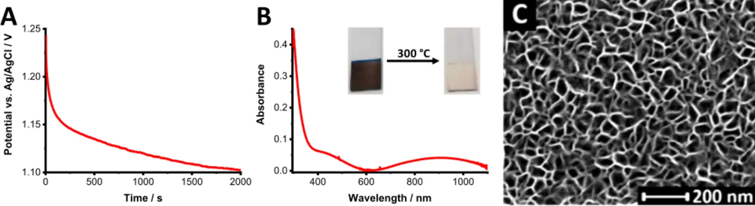
Figure 1A shows a galvanostatic deposition curve, recorded at 0.5 mA cm−2current density. There was only a minor change in the de- position potential through the synthesis, indicating the steady growth of the film. The formed nickel oxide hydroxide layers were black after the deposition, and became almost transparent after the heat-treatment at 300°C. The UV–vis spectrum of an annealed layer is shown in Fig- ure1B. One sharp band appeared in the near UV region and there are other two broad bands in the visible and near-infrared regime.
The bandgap, which was determined from diffuse reflectance spec- trum using Tauc conversion for an indirect transition, gave a value of 3.50 eV (Figure S1), in close agreement with values reported in the literature.24Scanning electron microscopic (SEM) image (Figure 1C) showed that a homogeneous nanostructured film formed on the surface of the ITO electrode, which is highly porous and composed of interconnected nanoflakes. The pore size was 46.6±11.9 nm, the wall thickness averaged at 13.1±1.7 nm. The layer thickness was 840± 60 nm, as determined from side-view, cross-section SEM images (not shown here).
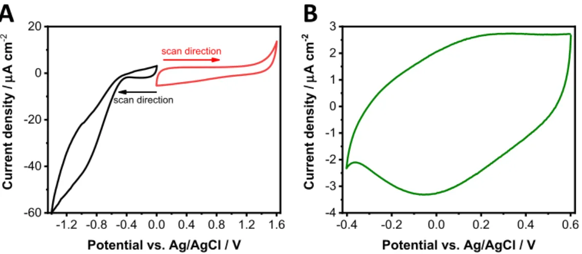
In the first step, the NiO layers were investigated in a non-aqueous solution. Potentiodynamic cycles were recorded to find the stability window of the NiO electrodes (Figure2A). While the cathodic current started to increase with an onset of∼−0.4 V, the film seemed to be stable toward oxidation. Cyclic voltammograms were recorded in a narrower potential range as well (between−0.4 and+0.6 V), to visu- alize the otherwise barely visible and broad redox peaks (Figure2B).
Note that these less pronounced redox events seem to be surface con- fined, while the higher currents outside this window are related to the transformation of the bulk material. Redox waves were observed during both the anodic and cathodic half-cycles related to Ni(II)→ Ni(III)+e− reaction on the surface.24,29 The oxidation peak onset was around 0.00 V which was difficult to determine due to the large capacitive loop.
Spectroelectrochemical experiments were performed to examine the absorbance changes of NiO films during cycling. The potential was scanned from 0.0 V with a sweep rate of 5 mV s−1 in both cathodic and anodic directions on two separate layers (Fig.2A). In the negative potential regime, the current started to increase from
0 500 1000 1500 2000
1.10 1.15 1.20 1.25
Potential vs. Ag/AgCl / V
Time / s
A
400 600 800 1000
0.0 0.1 0.2 0.3 0.4
Absorbance
Wavelength / nm
B
300 °C
Figure 1. A:Galvanostatic deposition curve of nickel oxide hydroxide at a current density of 0.5 mA cm−2.B:UV–vis absorbance spectrum, andC:SEM image of the electrodeposited NiO electrode after the heat-treatment at 300°C for 60 min.
-1.2 -0.8 -0.4 0.0 0.4 0.8 1.2 1.6 -60
-40 -20 0 20
scan direction
Current density / µA cm-2
Potential vs. Ag/AgCl / V
scan direction
-0.4 -0.2 0.0 0.2 0.4 0.6
-4 -3 -2 -1 0 1 2 3
Current density / µA cm-2
Potential vs. Ag/AgCl / V
A B
Figure 2. Cyclic voltammograms of the heat-treated ITO/NiO electrodes.A:The reduction (black) and the oxidation (red) cycle.B:CV scan recorded in a narrower potential range. All measurements were carried out in deaerated 1 mol dm−3LiClO4/acetonitrile electrolyte.
−0.4 V (black curve on Figure2A). The absorbance difference spectra (Figure3A), however, show a very different potential dependence. The absorbance decreases until−0.4 V and then remained constant upon polarizing the electrode to more negative potentials (where the higher cathodic current flows). Notably, the blank spectrum was recorded from the sample held at open circuit potential, which was around 0.5 V. Because of the heat-treatment in air at 300°C, the layers contained Ni(III) traces at the surface, which give a brownish tint of the oth- erwise fully transparent NiO films. This color gradually disappeared when the potential was changed toward the negative direction. Un- der positive bias (red curve on Figure2A), the most pronounced ab- sorbance change was at 370 nm, which decreased gradually at higher
wavelengths (Figure3B). Upon oxidation, there was an absorbance increase, which was perfectly reversible upon subsequent reduction.
To highlight the changes in the optical properties, the absorbance at 370 nm was plotted as a function of time (Figures3Cand3D). These optical changes were attributed to the oxidation of Ni(II) at the surface to Ni(III) and then possibly to Ni(IV).24,30
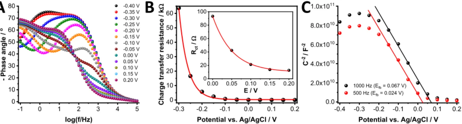
Electrochemical impedance spectroscopic measurements were performed to investigate the electronic properties of NiO electrodes under different charging/discharging conditions. Both the shape of the Bode plots (Figure4A) and the charge transfer resistance (Fig- ure4B) changed as a function of the potential (between−0.30 and 0.10 V). Based on the careful investigation of these two figures, several
Figure 3. Spectroelectrochemical data of ITO/NiO electrodes, recorded in 1 mol dm−3LiClO4/acetonitrile electrolyte (5 mV s−1sweep rate), duringA:reduction andB:oxidation half cycles. Change of the absorbance at 370 nm during two cycles in theC:negative andD:positive potential regime.
Figure 4. Electrochemical impedance spectroscopic measurements: A: Bode-plot of ITO/NiO electrodes recorded in oxygen-saturated 1 mol dm−3 LiClO4/acetonitrile electrolyte at different potentials.B:Charge transfer resistance as a function of the applied potential. C:Mott-Schottky plots at two different frequencies.
important conclusions can be drawn. The phase angle minimum in the Bode plot is associated with a capacitance and a resistance pair. These are related to each other, thus they cannot be separated. The appear- ance or disappearance of the minima are the consequence of the de- crease in the resistance or the capacitance. There are two characteristic changes in Fig.4A: (i) the decay of the first phase angle minimum in the−0.3 V to+0.1 V potential range, (ii) a new minimum developing at more positive potentials (from−0.10 V). The first change occurs in the same potential range where the charge transfer resistance de- creases, as shown in the respective Nyquist plot (Figure S2), and also calculated from the electrochemical circle fit (Figure4B). The second change (from−0.10 V) corresponds to appearance of Ni(III) on the surface. Overall, deconvolution of these complex trends suggests that in addition to the electrochemical reaction happening on the surface (Ni(II)/Ni(III)), trap states also have a role in changing the charge transfer resistance.
To determine the flatband potential of NiO, Mott−Schottky anal- ysis was carried out at two different frequencies (Figure4C). The average value of the flatband was 0.046± 0.022 V (vs. Ag/AgCl) which is in good agreement with the onset potential of the photocur- rent (∼0.0 V vs. Ag/AgCl, see Figure S3). Note that the change in theRct value starts exactly at this potential (Fig.4B). At potentials more negative than the flatband, the majority carriers (holes) cannot reach the electrode/electrolyte interface. In other words, when the trap states close to the valence band edge are populated with electrons, the electron-accepting property of NiO decreases substantially, then theRctincreases (see also discussion on Figure6later). At more posi- tive potentials (where the surface oxidation of NiO occurs), however, the resistance value remains unchanged.
To further investigate the changes in the electronic structure and the structural features of the NiO layersas a function of potential, in situ Raman spectroelectrochemistry was performed (Figure5A).
During these experiments the applied bias potential was varied in a non-orderly manner in the range from –0.4 to+0.7 V vs. Ag/AgCl, to simultaneously confirm the reversibility of the measurements. The broad band at∼500 cm−1corresponds to the longitudinal optical (LO) phonon mode of NiO,31,32while the other peaks in the Raman spectra are due to the electrolyte and the sapphire window (Figure S4).33–35 This phonon mode originated from the nickel vacancy defects due to the non-stoichiometric Ni–O stretching vibrations.36By applying positive bias, a gradual increase in the intensity of the LO mode was observed, while the intensity of the other bands remained constant.
This trend confirms that defect states are introduced upon oxidation.
The normalized intensity of the 500 cm−1peak is plotted as a func- tion of the potential in Fig.5B. Between−0.4 and 0.0 V the slope of the intensity increase was considerably smaller, compared to the one between 0.0 V to 0.7 V. These results confirm that before the electro- chemical reaction (in the−0.4–0.0 V potential region) there is another process, which affects the Raman intensity of the LO mode of NiO, although to a minor extent.
To further prove that the population/depopulation of the trap states affects the electronic properties, DOS plots were measured for an as- synthesized layer and for oxidized/reduced ones as well (after applying a pre-conditioning for 5 min). After recording the DOS plot of the as- is film, the trap states were filled with electrons by the treatment at
−0.4 V (as seen from the increased electron density in Figure6A).
After polarizing the electrode at+0.6 V, the DOS plot was similar to that of the as-synthesized layer, confirming that the previously filled
400 600 800 1000 1200
sapphire glass (~418 cm-1) perchlorate (~625 cm-1) perchlorate (~935 cm-1)
acetonitrile (~923 cm-1)
sapphire glass (~750 cm-1) acetonitrile (~382 cm-1)
~500 cm-1 (1LO)
Normalized Raman intensity
Raman shift / cm-1
(a) -0.4 V (b) -0.3 V (c) -0.2 V (d) -0.1 V (e) 0.0 V (f) 0.1 V (g) 0.2 V (h) 0.3 V (i) 0.4 V (j) 0.5 V (k) 0.6 V (l) 0.7 V
a) l)
-0.4 -0.2 0.0 0.2 0.4 0.6
Band at 500 cm-1
Normalized Raman intensity
Potential vs. Ag/AgCl / V
A B
Figure 5. A:In situ Raman spectroelectrochemistry of the NiO layer in 1 mol dm−3LiClO4/acetonitrile electrolyte.B:Normalized Raman intensity as a function of the applied potential.
A B
-6.5 -6.0 -5.5 -5.0 -4.5
Density of states / a.u.
Energy / eV vs. vacuum
Deposited layer After 300 s at -0.40 V After 300 s at +0.60 V
0.0 0.1 0.2 -6
-5 -4 -3
-2 ECB
EVB
Energy / eV vs. vacuum
Normalized DOS
conductivity change absorbance change starts
0 -1 -2 -3
Potential / V vs. Ag/AgCl
Figure 6. A:Density of states plots of NiO layers treated at selected potential values for 5 min, in 1 mol dm−3LiClO4/acetonitrile. The filled area represents the relative density of states at different energy levels.B:Band energy diagram of NiO together with the density of states plot which was measured after the potentiostatic conditioning at –0.4 V. The potential range of the electrical changes and the onset potential of the optical changes are also marked.
state can be depleted at+0.6 V. The valence band position of NiO was at−5.42 eV, as determined by APS (Figure S5B). The Fermi level was close to the valence band, as confirmed by the contact potential difference measurement (EF= −5.06 eV, see Figure S5A). This is not surprising, considering that NiO is a p-type semiconductor. Using the optical bandgap value (determined from Tauc plot derived for an indirect allowed transition), the band energy diagram was constructed (Fig.6B).37,38Figure6Bincludes also the DOS plot, measured after a potentiostatic conditioning at−0.40 V. The potential windows of the optical and electrical changes are shown also on this diagram.
The charge transfer resistance changed within a well-defined potential range close to the valence band edge, which indicates that this change is caused by the population/depopulation of shallow trap states. For example, upon oxidation, as gradually less electrons are present on these states, theRct of majority carriers (holes) decreases (consider the ease of electron transfer from the solution to an unoccupied state).
The change of the absorbance started from less negative potential and increased continuously toward more positive potentials, indicating that these changes are not connected to discrete energy levels.
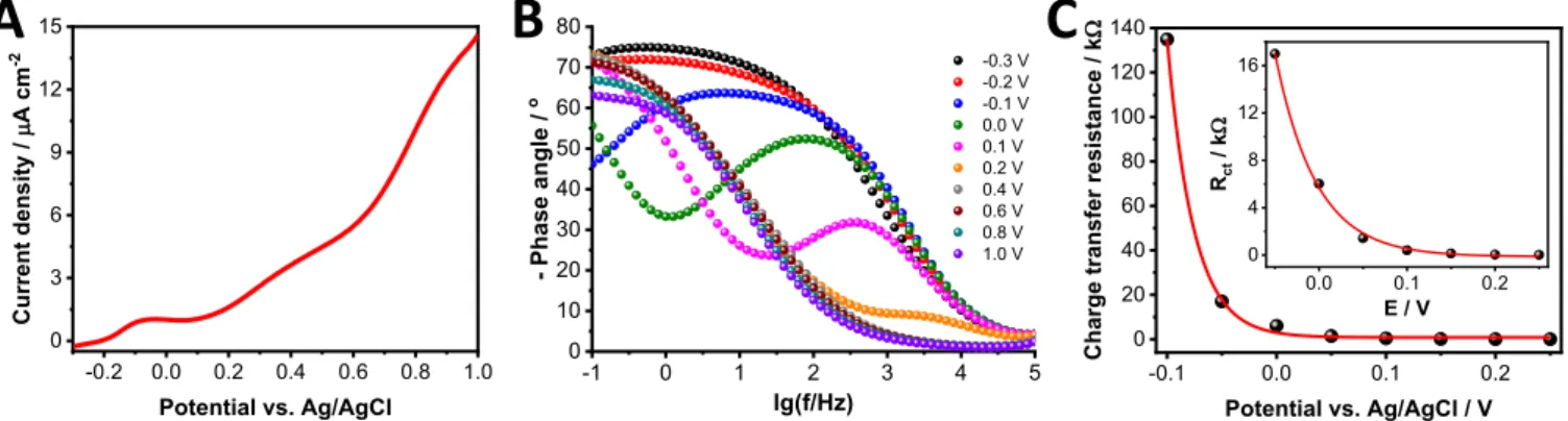
We aimed to examine whether the presented phenomena are con- fined to organic media only or similar trends can be seen in an aqueous electrolyte (0.1 mol dm−3Na2SO4). Although the current response on Figure7Ais dominated by the electrical double-layer capacitance of the NiO film,25the observed redox waves are more distinct than those seen in non-aqueous electrolyte. The first oxidation peak developed at
∼0.2 V while a second peak started to appear at∼0.6 V which are the same values as in the literature at pH=7.24More interestingly, an ad- ditional peak can be observed with the maximum at−0.1 V, which is
related to the electron removal from the trap states close to the valence band. The magnitude of this redox wave depends of the potentiostatic pretreatment time at cathodic bias (−0.3 V): the more electrons are injected to the trap states, the more charge it takes to remove them.
The absorbance features are very similar to the measurements in non- aqueous solution with the exception that the absorbance maximum was around 340 nm (Figure S6).
As discussed above, the first faradaic event in aqueous media oc- curs with the onset of 0.2 V. This was also proven by in situ Raman spectroelectrochemistry (Figure S7), where the LO mode started to increase at the exact same potential. The electronic properties, how- ever, are already changed at this potential. This is reflected both in the shape of the Bode plots (Figure7B) and in the charge transfer resis- tance values (Figure7C) (the Nyquist plots are shown in Figure S8).
After 0.2 V, the charge transfer resistance does not change with the applied potential.
Conclusions
The role of trap states on the optoelectronic properties of elec- trodeposited nanoporous NiO films was probed by in situ combined electrochemical methods, both in non-aqueous and aqueous media. We demonstrated that beside the electrochemical reaction (Ni(II)/Ni(III)), which is responsible for the optical changes, the electron depopulation of trap states causes an abrupt decrease in the charge transfer resistance upon oxidation. Specifically, electron injection into the layer at poten- tials below the flatband results in higher charge transfer resistance. The reason behind this effect was unveiled by recording density of states
Figure 7. A:Linear sweep voltammogram recorded with a sweep rate of 5 mV s−1.B:Bode plot of ITO/NiO electrodes recorded at different potentials.C:Charge transfer resistance as a function of the applied potential. All measurements were carried out in oxygen-saturated aqueous 0.1 mol dm−3Na2SO4electrolyte.
plots, where a remarkable electron density appeared above the va- lence band edge upon a reductive treatment at−0.4 V (vs. Ag/AgCl).
Raman spectroelectrochemistry measurements confirmed that two separate processes occur as a function of the potential: one related to the redox transformation of NiO, and another one related to the population/depopulation of shallow trap states.
Acknowledgments
This project has received funding from the European Research Council (ERC) under the European Union’s Horizon 2020 research and innovation program (grant agreement No 716539). Ministry of Human Capacities, Hungary grant 20391–3/2018/FEKUSTRAT is also acknowledged. and the “Sze´chenyi 2020” program in the frame- work of GINOP-2.3.2-15-2016-00013. The authors thank Dr. Gergely F. Samu and Dr. Bíborka Janáky-Bohner for their constructive criti- cism and support in the manuscript preparation.
ORCID
Csaba Janáky https://orcid.org/0000-0001-5965-5173
References
1. C. Visy,In situ Combined Electrochemical Techniques for Conducting Polymers, Springer, Cham, (2017).
2. R. O. Lezna, R. Romagnoli, N. R. de Tacconi, and K. Rajeshwar,J. Electroanal.
Chem.,544, 101 (2003).
3. C.-H. Pyun and S.-M. Park,J. Electrochem. Soc.,133, 2024 (1986).
4. C. Zhang and S.-M. Park,J. Electrochem. Soc.,134, 2966 (1987).
5. J. W. Long, A. L. Young, and D. R. Rolison,J. Electrochem. Soc.,150, A1161 (2003).
6. N. R. De Tacconi, K. Rajeshwar, and R. O. Lezna,J. Phys. Chem.,100, 18234 (1996).
7. G. Boschloo and D. Fitzmaurice,J. Phys. Chem. B,103, 7860 (1999).
8. L. Kavan and M. Grätzel,Electrochim. Acta,40, 643 (1995).
9. G. Boschloo and D. Fitzmaurice,J. Phys. Chem. B,103, 2228 (1999).
10. E. ´Swi ˛etek, K. Pilarczyk, J. Derdzi´nska, K. Szaciłowski, and W. Macyk,Phys. Chem.
Chem. Phys.,15, 14256 (2013).
11. T. Berger, J. A. Anta, and V. Morales-Flórez,J. Phys. Chem. C,116, 11444 (2012).
12. S. Volk, N. Yazdani, E. Sanusoglu, O. Yarema, M. Yarema, and V. Wood,J. Phys.
Chem. Lett.,9, 1384 (2018).
13. R. Beranek,Adv. Phys. Chem.,2011, 1 (2011).
14. M. Kobielusz, K. Pilarczyk, E. ´Swi ˛etek, K. Szaciłowski, and W. Macyk,Catal. Today, 309, 35 (2018).
15. P. S. Tóth, E. Peintler-Kriván, and C. Visy,Electrochem. commun.,12, 958 (2010).
16. E. Peintler-Kriván, P. S. Tóth, and C. Visy,Electrochem. commun.,11, 1947 (2009).
17. J. He, H. Lindström, A. Hagfeldt, and S.-E. Lindquist,J. Phys. Chem. B,103, 8940 (1999).
18. J. R. Manders, S. Tsang, M. J. Hartel, T. Lai, S. Chen, C. M. Amb, J. R. Reynolds, and F. So,Adv. Funct. Mater.,23, 2993 (2013).
19. K.-C. Wang, J.-Y. Jeng, P.-S. Shen, Y.-C. Chang, E. W.-G. Diau, C.-H. Tsai, T.-Y. Chao, H.-C. Hsu, P.-Y. Lin, P. Chen et al.,Sci. Rep.,4, 4756-1−4756-8 (2015).
20. M.-S. Wu and C.-H. Yang,Appl. Phys. Lett.,91, 033109 (2007).
21. Y. F. Yuan, X. H. Xia, J. B. Wu, Y. B. Chen, J. L. Yang, and S. Y. Guo,Electrochim.
Acta,56, 1208 (2011).
22. D. A. Wruck and M. Rubin,J. Electrochem. Soc.,140, 1097 (1993).
23. D. M. Tench, E. Yeager, I. February, G. J. Hills, J. E. Oxley, and D. W. Turner, J. Electrochem. Soc.,120, 164 (1973).
24. G. Boschloo and A. Hagfeldt,J. Phys. Chem. B,105, 3039 (2001).
25. M. S. Wu, Y. A. Huang, C. H. Yang, and J. J. Jow,Int. J. Hydrogen Energy,32, 4153 (2007).
26. M.-S. Wu, C.-H. Yang, and M.-J. Wang,Electrochim. Acta,54, 155 (2008).
27. A. Kormányos, D. Hursán, and C. Janáky,J. Phys. Chem. C,122, 13682 (2018).
28. I. D. Baikie, A. C. Grain, J. Sutherland, and J. Law,Appl. Surf. Sci.,323, 45 (2014).
29. F. Odobel, Y. Pellegrin, E. A. Gibson, A. Hagfeldt, A. L. Smeigh, and L. Hammarström,Coord. Chem. Rev.,256, 2414 (2012).
30. L. D’Amario, R. Jiang, U. B. Cappel, E. A. Gibson, G. Boschloo, H. Rensmo, L. Sun, L. Hammarström, and H. Tian,ACS Appl. Mater. Interfaces,9, 33470 (2017).
31. G. Zhou, D. Wang, L. Yin, N. Li, F. Li, and H. Cheng,ACS Nano,6, 3214 (2012).
32. W. Wang, Y. Liu, C. Xu, C. Zheng, and G. Wang,Chem. Phys. Lett.,362, 119 (2002).
33. L. T. Costa, L. J. A. Siqueira, B. G. Nicolau, and M. C. C. Ribeiro,Vib. Spectrosc., 54, 155 (2010).
34. J. C. Deàk, L. K. Iwaki, and D. D. Dlott,J. Phys. Chem. A,102, 8193 (1998).
35. M. Kadleı´ková, J. Breza, and M. Veselý,Microelectronics J.,32, 955 (2001).
36. D. Y. Jiang, J. M. Qin, X. Wang, S. Gao, Q. C. Liang, and J. X. Zhao,Vacuum,86, 1083 (2012).
37. M. D. Irwin, D. B. Buchholz, A. W. Hains, R. P. H. Chang, and T. J. Marks,Proc.
Natl. Acad. Sci.,105, 2783 (2008).
38. T. Xie, G. Liu, B. Wen, J. Y. Ha, N. V. Nguyen, A. Motayed, and R. Debnath,ACS Appl. Mater. Interfaces,7, 9660 (2015).