ARTICLE
OPENGiant shift upon strain on the fl uorescence spectrum of V N N B color centers in h -BN
Song Li 1, Jyh-Pin Chou 1, Alice Hu1, Martin B. Plenio2, Péter Udvarhelyi3,4, GergőThiering3, Mehdi Abdi5and Adam Gali 3,6✉
We study the effect of strain on the physical properties of the nitrogen antisite-vacancy pair in hexagonal boron nitride (h-BN), a color center that may be employed as a quantum bit in a two-dimensional material. With group theory and ab initio analysis we show that strong electron–phonon coupling plays a key role in the optical activation of this color center. Wefind a giant shift on the zero-phonon-line (ZPL) emission of the nitrogen antisite-vacancy pair defect upon applying strain that is typical ofh-BN samples.
Our results provide a plausible explanation for the experimental observation of quantum emitters with similar optical properties but widely scattered ZPL wavelengths and the experimentally observed dependence of the ZPL on the strain.
npj Quantum Information (2020) 6:85 ; https://doi.org/10.1038/s41534-020-00312-y
INTRODUCTION
Quantum emissions from two-dimensional (2D) materials have recently received considerable and rapidly rising interest of researchers in both condensed matter and quantum optics1–3 as these systems provide a potential basis for emerging technologies such as quantum nanophotonics4–6, quantum sensing7–9, and quantum information processing10,11. The observation of single- photon emitters (SPEs) in hexagonal boron nitrite (h-BN) has added a fascinating new facet to the researchfield of layered materials12. The wide band gap ofh-BN makes it an insulator that can host high- quality emitters and allows for combination with other materials as substrates13. The experiments for exploring the nature of the emission of these color centers started with their first observa- tions10,14–25and recent theoretical works have provided evidence that the SPEs are indeed color centers, i.e., local point defects26–30. Despite the considerable efforts that have been directed at the experimental exploration of these SPEs so far, a thorough theoretical understanding of the properties of the emitters that have been experimentally observed remains to be developed. Especially, the fact that many emitters appear at the edges ofh-BN flakes and wrinkles on them31,32motivates the investigation on the effect of strain on these emitters. Furthermore, the quantum emitters have shown magnetic properties in some experiments33–36, while in other experiments non-magnetic behavior was found21.
The most commonly observed quantum emitters exhibit emission in the visible, where competing for theoretical mod- els27,37 exists in the literature. It has been suggested recently, based on the similarities of the optical lifetimes of the observed quantum emitters38, that two types of quantum emitters in the visible region may occur inh-BN, and the widely scattered zero- phonon-line (ZPL) energies might be attributed to external perturbations. One of the key candidates for this external perturbation is the local strain that may vary significantly in the h-BN samples, in particular, in polycrystalline h-BN samples. In another recent work, on the other hand, four different types of emitters have been found by means of combined chatodolumi- nescence and photoluminescence study where the applied stress did not change the brightness of emitters and the shift in ZPL was
in the 10 meV region39. Yet another experiment also found a relatively small shift upon applied stress on a given emitter40.
These seemingly contradictory observations and the lack of a conclusive theoretical prediction motivates the study of the effect of strain on point defects inh-BN based on the assumption that point defects are the origin of the observed quantum emitters. Further- more, a thorough understanding of the electron–strain coupling properties also forms a rigorous theoretical basis for proposed spin- and electro-mechanical systems for control and manipulation of a mechanical resonator by means of spin-motion coupling11,41,42. Group-theory analysis in combination with ab initio Kohn–Sham density functional theory (DFT) simulations can be a very powerful tools for understanding the coupling between optical emission and strain. So far the electron-strain coupling inh-BN emitters has been studied with limited accuracy40by monitoring only the change in Kohn–Sham levels and the states that do not directly provide the ZPL energy in the PL spectrum monitored in the experiments.
Here we study the effect of strain on the ZPL emission of a key color center inh-BN, the nitrogen antisite-vacancy pair defect, by means of group theory and advanced DFT calculations, which can act as a quantum emitter with exhibiting a ZPL emission at around 1.9 eV (645 nm)27. We report a giant, 12 eV/strain ZPL-strain coupling parameter for this quantum emitter which results in about 100 nm scattering of the ZPL emission with ±1% strain in h-BN sample. The physical origin of this giant effect is the strong electron–phonon coupling in h-BN. This result implies that local perturbations for vacancy type defects can seriously affect their optical spectrum and provide an explanation for the zoo of reported quantum emitters in the visible region.
RESULTS AND DISCUSSION
Group theory and DFT calculation analysis
The sensitivity of the optical ZPL emission to the applied local strain greatly depends on the microscopic configuration of the point defect in h-BN. Here, we put our focus on the neutral nitrogen antisite-vacancy pair defect, VNNB, which was first suggested as a candidate of the observed single-photon
1Department of Mechanical Engineering, City University of Hong Kong, Hong Kong, SAR, China.2Institute of Theoretical Physics and IQST, Ulm University, Albert-Einstein-Allee 11, Ulm 89069, Germany.3Wigner Research Centre for Physics, P.O. Box 49, Budapest H-1525, Hungary.4Eötvös Science University, Pázmány Péter Sétány 1/A, Budapest H-1117, Hungary.5Department of Physics, Isfahan University of Technology, Isfahan 84156-83111, Iran.6Budapest University of Technology and Economics, Budafoki út 8, Budapest H-1111, Hungary.✉email: gali.adam@wigner.hu
1234567890():,;
emissions10 and then thoroughly studied as one of the feasible quantum emitter in the visible with S=1/2 spin state27. The optical properties of this defect have been examined from various theoretical methods and point of view27,43–45. The defect has a C2v
symmetry before the relaxation of the atoms in monolayerh-BN, and introduces three levels in the energy band gap that are labeled as a1, b2 and b02 owing to their irreducible symmetry representation. These energy levels are occupied by three electrons resulting a2B2many-electron ground state (see Figs.1 and2). In this paper, we use majuscule and minuscule to labels the symmetry of the many-elctron states and one-electron levels, respectively. The two lowest-energy spin-preserving optical transitions are the following: in the spin majority channel the electron fromb2may be promoted tob02or in the spin minority channel the electron froma1may be promoted tob2. It is found that thea1↔b2has lower energy thanb2$b0227,43,44. However, for the defect with the C2v symmetry, the a1 ↔ b2 optical transition has a very small optical transition in-plane dipole moment44. Indeed, we also find this behavior in our own DFT calculation (see Supplementary Fig. S1). We indeed notice thatb2
and b02 states have wavefunctions that extend out-of-plane (see Fig.1b), and therefore, can couple to phonon modes that drive the atoms out-of-plane, the membrane modes. There is an unpaired electron in bothB2ground state andB02excited state placed on the b2 and b02 orbital, respectively, that induce an out-of-plane geometry distortion. These phonon modes strongly couple the2B2
ground state and the 2A1 excited state leading to the vibronic instablility of the ground state. Therefore, the defect does not preserve the planar structure and the nitrogen antisite moves out from the plane in the ground state reducing the symmetry of the defect to Cs(see Fig.1a). This geometry is about 100 meV lower in energy than the C2v configuration which reveals the strong coupling of the defect electrons to the membrane mode phonons.
This result basically agrees with previous DFT calculations46. In Cs symmetry, all the one-electron defect levels belong to a0 irreducible representation. Despite the vibronic mixing, the correspondence to the high symmetry orbitals can be observed
in Fig.1b and c. When the hole is left ata1orbital in theA1excited state, then the coupling to the membrane phonons is negligible and the defects C2v symmetry is retrieved. For the sake of simplicity, here we use the C2v symmetry labels for both configurations. The transformation of the point symmetry of the defect is discussed in Supplementary Note 1.
Owing to the rearrangement of the ions, the B2(Cs)↔A1(C2v) optical transition assumes a dipole moment symmetry similar to that of B2ðCsÞ $B02ðCsÞ transition (see Supplementary Note 2).
This becomes clear from Fig.1c where the wavefunctionsb2and a1 are shown for the Cs configuration. In fact, both of them transform asA0in the Csconfiguration, and therefore, are coupled via the in-plane (the stronger component) polarization. As a consequence, the lowest-energyfluorescence is expected to occur as a radiative decay from the A1(C2v) excited state to theB2(Cs) ground state becauseA1excited state has lower energy than that ofB02excited state27. This result constitutes the optical activation of a color center inh-BN by means of a strong electron–phonon coupling. Consequently, it becomes important to study the strain dependence of the ZPL emission for theB2(Cs)↔A1(C2v) optical transition. Details on the strain dependence for the higher energy transition is shown in the Supplementary Note 3.
It is intriguing to carry out group theory analysis before starting the numerical ab initio calculations. The detailed general description about the multi-electron configurations and their interaction with strain can be found in the “Methods”, that we apply to the VNNBquantum emitter. The analysis is performed for the C2v symmetry as the excited state transforms within C2v symmetry whereas the Csground state follows the same analysis taking into account the fact that Cs is a subgroup of the C2v symmetry. Within C2vsymmetry for the axial strain, the ZPL shift upon strain is given by
δ¼^εA1hhb2jΔ^A1jb2i ha1jΔ^A1ja1ii
; (1)
where^εA1is the strain tensor applying the strain parallel to theC2
symmetry axis (axial strain) andΔ^A1 is associated with the energy shifts for the corresponding electronic states (see“Methods”). The Cs configuration can then be described as an out-of-plane distortion due to a built-in strain that acts perpendicular to the basal plane. This mixesa1andb2orbitals throughB2component of the strain as explained in“Methods”. Since the energy spacing between the a1 and b2 levels is much larger than the typical deformation values this mixture should not significantly alter the energy shift ofδupon applying basal uniaxial strain. Hence, the energy shift in Eq. (1) is a good approximation. This ZPL energy shift is expected to depend linearly on strain for the B2(Cs) ↔ A1(C2v) optical transition. The magnitude of the strain-ZPL coupling as a function of the orientation of the applied uniaxial strain cannot be determined by means of group theory. We, therefore, apply DFT simulations to quantify the strength of the strain-ZPL coupling for VNNBemission.
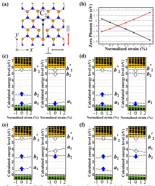
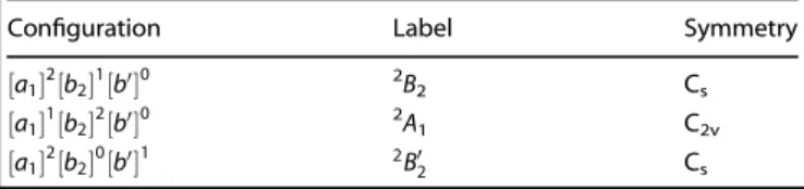
We calculate the ZPL energy as the total energy difference between the excited state and the ground state in the global energy minimum of the corresponding electronic configuration (see “Methods”). The strain is modeled by changing the lattice constant of the employed supercell (see Fig.2a, where the parallel (red) and perpendicular (black) components of the strain are depicted). The corresponding curves for the ZPL shift are plotted in Fig.2b as a function of the applied strain. The calculated ZPL of VNNB without strain is 1.90 eV for the B2(Cs) ↔ A1(C2v) optical transition, which is very close to the observed photoemission at 1.95 eV of certain SPEs14,17. As expected, the curves are quasi- linear within (−1;+2)% strain region, where we use−and+for compressive and tensile strain, respectively. For both strain directions, we obtain a giant, 12 eV/strain shift in the ZPL energy which results in a huge variation in the emission wavelength as a Fig. 1 Defect orbitals of VNNB defect. aThe geometry of VNNB
defect in the ground state. Top view (left) and side view (right). The dashed circle denotes the impurity nitrogen atom. The defect is out- of-plane and exhibits Cs symmetry. The red arrows indicate the direction of the phonon vibration.bThea1,b2andb02defect states in C2vgeometry.cThe defect states in the Cssymmetry with the same energy order as those in (b). While in C2vsymmetry onlyb2
state has components out-of-plane, it can be seen that in Cs symmetry thea1state also gains an out-of-plane component.
2
1234567890():,;
function of strain. For this quantum emitter, the tensile axial (perpendicular) uniaxial strain causes blueshift (redshift) in the ZPL emission. The variation of the ZPL energy with strain is about 100 nm and we believe our proposed mechanism yields the most plausible explanation for the observed variation of ZPL energies for certain SPEs.
In order to further study these results, we plot the shift of the defect levels upon the applied strain in the corresponding ground and excited states in Fig.2c–f. Upon applying tensile axial strain, thea1level in the ground state shifts down whereas the occupied b2level shifts up in the ground and excited electronic configura- tions, respectively. This will result in a blueshift in the ZPL. Upon applying tensile perpendicular strain, thea1level shifts up steeply whereas the occupiedb2level moderately shifts up in the ground and excited electronic configurations, respectively. As a conse- quence, the two levels approach each other upon applying this strain which results in a redshift in the ZPL energy. This is in agreement with the observations reported in ref.40where the ZPL
energy shift of the studied emitters exhibits a linear dependence on the applied strain. Furthermore, the three different possible orientations of the defect axis and our results on the blueshift (redshift) of the emission line for armchair (zigzag) strain explains the experimentally observed behavior40.
Role of membrane phonons
Wefind that the phonon modes with atoms moving out-of-plane, i.e., membrane modes, play a crucial role in the optical activation of the VNNB defect in h-BN (see Supplementary Note 4). The modes are mainly contributed from the substitutional nitrogen atom. These membraneB2phonons couple the2A1excited state and2B2ground state where the ground state will be unstable at the C2vsymmetry configuration and is distorted to Csconfigura- tion, whereas the excited state remains stable at C2vconfiguration.
This suggests a strong pseudo Jahn–Teller (PJT)47system which is illustrated in Fig.3a.
Calculated energy level (eV)
(a) (b)
Calculated energy level (eV) Calculated energy level (eV) Calculated energy level (eV)
(c)
Calculated energy level (eV) Calculated energy level (eV) Calculated energy level (eV) Calculated energy level (eV)
-1 0 1 2
Normalized strain (%)
b'
2b
2a
1(d)
-1 0 1 2
Normalized strain (%)
b'
2b
2a
1b'
2b
2a
1-1 0 1 2
Normalized strain (%)
-1 0 1 2
Normalized strain (%)
-1 0 1 2
Normalized strain (%)
-1 0 1 2
Normalized strain (%)
-1 0 1 2
Normalized strain (%)
-1 0 1 2
Normalized strain (%)
(e) (f)
b'
2b
2a
1b'
2b
2a
1b'
2b
2a
1b'
2b
2a
1b'
2b
2a
1Normalized strain (%)
Zero Phonon Line (eV)
x y
C
2Fig. 2 Zero-phonon-line energies upon strain for VNNBdefect. aThe simplified cartoon of VNNBdefect inh-BN. The defect is not planar and exhibits Cssymmetry in the ground state. The black and red arrow denote the directions of uniaxial strain perpendicular (⊥) and parallel (∥) to the C2main axis, respectively.bThe ZPL evolution as a function of external strain fora1tob2transition. The black and red lines denote the directions of strain perpendicular (⊥) and parallel (∥) directions. The energy level at ground state with Cssymmetry evolution as a function of external strain for perpendicular (c) and parallel (d) directions, respectively. The energy level at excited state (a1tob2) with C2vsymmetry evolution as a function of external strain for perpendicular (e) and parallel (f) directions, respectively. The left and right panels show, respectively, the results for the spin-up channel and spin-down channels.
3
We depict the adiabatic potential energy surface (APES) of the
2B2 ground state of VNNB in Fig. 3b as obtained by HSE DFT calculations. We note that DFT calculation with a less accurate semilocal functional than HSE (see“Methods”) obtained a similar APES in a previous study46. The Jahn–Teller energy is 95 meV. The solution of this strongly coupled electron–phonon system47is
ϵ±ðQÞ ¼1
2Mω2Q2±Δ2þF2Q212
; (2)
whereQis the normal coordinate of the effective phonon modeω with the corresponding massM,Δis the energy gap between the ground state and excited state at the high symmetry point (C2v configurations) andFis the strength of electron–phonon coupling.
In the dimensionless generalized coordinate system, we obtain F=178 meV and hω=23 meV. This electron-phonon coupling parameter is about 2.5× larger than that of NV center in diamond48. This indicates a giant electron-phonon interaction for the vacancy type defects in h-BN. We solved the electron- phonon PJT system quantum mechanically and found that the jumping rate between the two minima is 8.4 kHz. This is a relatively slow rate where the optical Rabi-oscillation between the ground and excited states should be more than two orders of magnitude faster (see Supplementary Note 5). This means that the ground state of2B2is a static PJT system, and the ground state indeed exhibits low Cssymmetry.
We note here that strong electron-phonon interaction with membrane phonons play an important role in the activation of intersystem crossing process in boron-vacancy optically detected magnetic resonance center49. This type of phonon modes can be found only in 2D solid-state systems. Thesefindings demonstrate that the membrane phonon modes are major actors in the magneto-optical properties of solid-state defect quantum bits and SPEs.
Comparison to known SPEs
Many SPEs were reported in multilayer h-BN structures. The physics of the membrane phonons and their effects on the optical properties for VNNBdefect are mainly discussed here based on the results achieved in monolayer h-BN, which directly models the single sheeth-BNflakes and can provide a tentative insight to the top layer of multilayeredh-BN structures. We extend our study to the bulkh-BN model (see“Methods”) which corresponds to such VNNB defects that are buried deep in the multilayer h-BN structures. Wefind that the physics of the membrane phonons is the same: PJT occurs in the presence of van der Waals interaction but it suppresses the Jahn–Teller energy to 50.5 meV.
Nevertheless, the resulting electron-phonon coupling remains strong withF=193 meV (see Supplementary Note 6). The weak interlayer interaction has little effect on the quantum emission of
VNNBas the ZPL energies and the ZPL energy shifts upon strain change <0.01 eV compared to the results obtained in the monolayerh-BN.
Most of the SPEs in h-BN were first observed at room temperature10,14 which emit in the visible region with various wavelength. Based on the ZPL emission region and the contribu- tion of the phonon sideband (PSB) to the total emission, the visible SPEs were categorized into two groups according to early measurements14: Group-1 with ZPL energies at 1.8–2.2 eV and with significant PSB contribution; Group-2 with ZPL energies at 1.4–1.8 eV with small PSB contribution. Group-1 emitters often showed an asymmetry in the ZPL lineshape at room temperature that was attributed to electron-phonon effects10. Recently, low- temperature observation challenged this idea where they could decompose the PL spectra into two emitter components that could naturally explain the asymmetry of the spectrum at elevated temperatures where the spectra of the two emitters cannot be resolved50. They found that the two emitters have ZPL energies with about 15 nm apart but very similar PSBs and also with a large variation of the ZPL wavelength of these pairs between 600 nm (2.06 eV) and 720 nm (1.72 eV) where the variation was tentatively attributed to strain50. Based on the calculated ZPL energy and strong electron-phonon coupling of the VNNB defect, the VNNB
definitely belongs to the Group-1 emitters and the calculated strain dependence of the calculated ZPL energies can cover the range of the observed ZPL energies by assuming about ±2% strain in the h-BN lattice. Parallel to our study, nanobeam electron diffraction has been applied to correlate the emitter optical emission with the emitter’s local in-plane strain and found that about ±2% local strain can appear in h-BN flakes39. They have found SPEs at 630 nm and 705 nm ZPL energies that are most likely connected by strain39. The VNNB defect can produce this giant shift of ZPL wavelength upon about 1.5% strain which is not far from the experimental observations claiming about 1%39. We note that unambiguous identification of the SPEs require further work from experiments and theory. Nevertheless, our study shows by means of accurate DFT calculations that the optical response of VNNBdefect to strain is indeed very sensitive. Further theoretical studies might reveal other defects inh-BN with similar properties.
Implications towards quantum information processing applications
The strong electron–phonon interaction implies that the optical properties of vacancy type quantum emitters in h-BN can vary significantly with strain. Indeed, our DFT simulations show a giant shift in the ZPL emission at strain values that can appear inh-BN.
Compared to the SPEs in three-dimensional (3D) materials such as diamond and SiC, the SPEs in 2D h-BN are not buried by high refractive index medium which makes collection efficiency of the emitted light much higher than that for 3D materials. Integration ofh-BN based SPEs with nanophotonic devices offers a promising path to engineer quantum gates and circuitry which are key building blocks of quantum information processing and our work provides crucial implications in this field. First, we report the activation of the forbidden optical transition due to the strong electron-phonon coupling. The electron-phonon coupling reduces the symmetry of the ground state of the defect and it is a static PJT system. Second, wefind the giant shift of the ZPL spectrum with external strain and propose a particular explanation for the phenomena. Until now, the spectral shift on SPEs in h-BN observed in our work is the largest known so far. Third, our result provides an analysis method for similar quantum emitters with varying ZPL energies and emission intensities in h-BN. Strain might be a reason for the spectral broadening and can influence the optical contrast and quantum efficiency. This might be harnessed to use this quantum emitter for realizing stress detector Fig. 3 Electron–phonon coupling of VNNB defect. a Pseudo
Jahn–Teller (PJT) effect between the excited state (red) and ground state (blue). Dashed line: before electron–phonon coupling; straight line: after electron–phonon coupling.ϵis the total energy of the system whereas Qis the selected configuration coordinate.bThe calculated adiabatic potential energy surface of the 2B2 ground state. The line is afit of PJT model (see text), where the resultant values are F=178 meV and hω=23 meV. The standard deviation is <2%.
4
at the nanoscale as well as nanomechanical devices for quantum technologies.
In this paper, we performed a thorough group theory analysis and DFT calculations on the effect of strain on nitrogen antisite- vacancy color center in h-BN. We find a very strong electron- phonon interaction that can activate photoluminescence, and is responsible for the giant ZPL shift upon the applied strain. The behavior of the strain-induced energy shift is correlated with the experimental observations further revealing their microscopic nature.
METHODS
Group theory analysis on strain
In this section, we provide a formulation that describes the effect of a local strain of the point defects. The derived Hamiltonian is general and is then applied to the VNNBquantum emitter inh-BN.
When considering point defects as candidates of the color centers inh- BN, the local strain manifests itself in modifying the atomic distances, which in turn, leads to the modification of the molecular orbitals (MOs) around the defect. Any change in the properties of MOs result-in a redistribution of the energy states in the band structure of the host solid.
Therefore, the strain directly couples to the electronic degrees-of-freedom of the color center. The coupling strength is called deformation potential.
We derive the Hamiltonian of the defect under local strain in the following way: We start by assuming that the color center is composed of Nevalance electrons that are mostly isolated from the rest of lattice and gather aroundNnnuclei forming up the defect. Note that this is a fairly good assumption by looking at the MOs drawn by DFT belonging to the defect states27. The attractive Coulomb energy imposed from nuclei on the electrons is then given by
VNe¼XNe
j¼1
XNn
k¼1
Vjkðxk;xjÞ X
j
X
k
Z0ke2
Rjk ; (3)
whereRjk=∣xk−xj∣withxkposition of the nuclei, whilexjdenotes the location of the jth electron. Here, Zk0 is the effective atomic number (screened nuclear charge) of the ion. The local strain displaces ions involved in the point defect x→x+δx and thus their Coulomb interaction. In the first order of accuracy we get VðjxxjÞ !VðjxþδxxjÞ VðRÞ þ½∇VðRÞ0δx, where δx is the infinitesimal displacement of the nuclei imposed by the local strain. The value of displacement is obtained byδx¼X^εwith the strain tensor^ε. The electron–strain interaction Hamiltonian is then summed over all such first-order variational terms
Hstr¼X
j;k ∇VðRjkÞ
0^εXk
X
j
X
α
Δ^αj^εα; (4)
where we have introducedΔ^j¼xjΞj, a dyadic whose components have different group symmetries denoted byα, whileΞj¼P
k 1 Rjk
∂Vjk
∂Rjk
h i
0xkis the deformation potential. Here, we have assumed that the radial component of the gradient is the dominant one and neglected an irrelevant constant term. The former is a valid assumption as the total Coulomb attraction of the ions is more or less a central force51–53.
The electronic configuration of this defect are given in Table1. Given the orbital symmetries of these states and the following table of symmetry for strain components the group theory can predict that the only non-zero irreducible representations of the Δ^ when sandwiched between two single-electron orbitals are:
The effect of strain on multi-electron states is a non-equal shift in their energy levels imposed by the axial components of the strain as well as inducing an interaction between the states via the axial and non-axial strain components. The amount of shift only depends on the electronic states and its relations for the ground and excited states areδ0,δ1, andδ2, respectively. The strain prompted inter-state interactions are much smaller than the energy difference between the levels, hence one neglects them in an adiabatic manner. The explicit form of the energy shifts are
δ0 ¼ ^εA0h2ha1jΔ^A0ja1i þ hb2jΔ^A0jb2ii
; δ1 ¼ ^εA1h2hb2j^ΔA1jb2i þ ha1jΔ^A1ja1ii
; δ2 ¼ ^εA0h2ha1j^ΔA0ja1i þ hb0jΔ^A0jb0ii
:
In the main text we have adopted the approximation that^εA0hjΔ^A0ji
^εA1hjΔ^A1jiwhich is reasonable owing to the fact that Csis a subgroup of C2vand that the molecular orbitals retain their form.
Details on DFT calculations
The calculations are performed based on the DFT implemented in Vienna ab initio simulation package (VASP)54,55. Projector augmented wave (PAW) is used to separate the valence electrons from the core part. The energy cutoff for the expansion of the plane-wave basis set was set to 450 eV which is enough to provide an accurate result. The screened hybrid density functional of Heyd, Scuseria, and Ernzerhof (HSE)56is used to calculate to band gap and defect levels. Within this approach, the short-range exchange potential is described by mixing with part of nonlocal Hartree–Fock exchange and this also provides reasonable geometry optimization of the dynamic Jahn–Teller system. The HSE hybrid functional with mixing parameter of 0.32 closely reproduces the experimental band gap at 5.9 eV. To apply the strain along the parallel and perpendicular directions to the C2 axis, a 9´5 ffiffiffi
p3
supercell is constructed through changing the basis to the orthorhombic structure. The perfect supercell contains 160 atoms which is sufficient to avoid the defect-defect interaction, and the singleΓ-point scheme is converged for the k-point sampling for the Brillouin zone. The coordinates of atoms are allowed to relax until the force is <0.01 eV/Å. The excited state was calculated within ΔSCF method57that we previously applied to point defects inh-BN too27. For the bulk simulation, a periodic model containing two layers are used, where one perfect layer is placed above the defective layer. The optimized interlayer distance is 3.37Åwith DFT-D3 method of Grimme58.
DATA AVAILABILITY
The data that support thefindings of this study are available from the corresponding author upon reasonable request.
Table 1. The configuration, symmetry, and spin multiplicity of the ground and two lowest excited states of neutral VNNB.
Configuration Label Symmetry
½a12½b21½b00 2B2 Cs
½a11½b22½b00 2A1 C2v
½a12½b20½b01 2B02 Cs
5
CODE AVAILABILITY
The codes that were used in this study are available upon request to the corresponding author.
Received: 18 December 2019; Accepted: 20 August 2020;
REFERENCES
1. Srivastava, A. et al. Optically active quantum dots in monolayer wse2. Nat.
Nanotechnol.10, 491–496 (2015).
2. Chakraborty, C., Kinnischtzke, L., Goodfellow, K. M., Beams, R. & Vamivakas, A. N.
Voltage-controlled quantum light from an atomically thin semiconductor.Nat.
Nanotechnol.10, 507–511 (2015).
3. Palacios-Berraquero, C. et al. Atomically thin quantum light-emitting diodes.Nat.
Commun.7, 12978 (2016).
4. Xia, F., Wang, H., Xiao, D., Dubey, M. & Ramasubramaniam, A. Two-dimensional material nanophotonics.Nat. Photon.8, 899 (2014).
5. Clark, G. et al. Single defect light-emitting diode in a van der waals hetero- structure.Nano Lett.16, 3944–3948 (2016).
6. Shiue, R.-J. et al. Active 2D materials for on-chip nanophotonics and quantum optics.Nanophotonics6, 1329–1342 (2017).
7. Lee, S. et al. Flexible organic solar cells composed of p3ht:pcbm using chemically doped graphene electrodes.Nanotechnology23, 344013 (2012).
8. Abderrahmane, A. et al. High photosensitivity few-layered mose2 back-gated field-effect phototransistors.Nanotechnology25, 365202 (2014).
9. Li, X., Yin, J., Zhou, J. & Guo, W. Large area hexagonal boron nitride monolayer as efficient atomically thick insulating coating against friction and oxidation.
Nanotechnology25, 105701 (2014).
10. Tran, T. T., Bray, K., Ford, M. J., Toth, M. & Aharonovich, I. Quantum emission from hexagonal boron nitride monolayers.Nat. Nanotechnol.11, 37 (2016).
11. Abdi, M., Hwang, M.-J., Aghtar, M. & Plenio, M. B. Spin-mechanics with color centers in hexagonal boron nitride membranes. Phys. Rev. Lett.119, 233602 (2017).
12. Aharonovich, I., Englund, D. & Toth, M. Solid-state single-photon emitters.Nat.
Photon.10, 631 (2016).
13. Golberg, D. et al. Boron nitride nanotubes and nanosheets. ACS Nano 4, 2979–2993 (2010).
14. Tran, T. T. et al. Robust multicolor single photon emission from point defects in hexagonal boron nitride.ACS Nano10, 7331 (2016).
15. Tran, T. T. et al. Quantum emission from defects in single-crystalline hexagonal boron nitride.Phys. Rev. Appl.5, 034005 (2016).
16. Jungwirth, N. R. et al. Temperature dependence of wavelength selectable zero- phonon emission from single defects in hexagonal boron nitride.Nano Lett.16, 6052 (2016).
17. Martinez, L. J. et al. Efficient single photon emission from a high-purity hexagonal boron nitride crystal.Phys. Rev. B94, 121405(R) (2016).
18. Schell, A. W., Tran, T. T., Takashima, H., Takeuchi, S. & Aharonovich, I. Non-linear excitation of quantum emitters in two-dimensional hexagonal boron nitride.ACS Photonics4, 761–767 (2017).
19. Shotan, Z. et al. Photoinduced modification of single-photon emitters in hex- agonal boron nitride.ACS Photonics3, 2490 (2016).
20. Jungwirth, N. R. & Fuchs, G. D. Optical absorption and emission mechanisms of single defects in hexagonal boron nitride.Phys. Rev. Lett.119, 057401 (2017).
21. Li, X. et al. Nonmagnetic quantum emitters in boron nitride with ultranarrow and sideband-free emission spectra.ACS Nano11, 6652–6660 (2017).
22. Exarhos, A. L., Hopper, D. A., Grote, R. R., Alkauskas, A. & Bassett, L. C. Optical signatures of quantum emitters in suspended hexagonal boron nitride.ACS Nano 11, 3328 (2017).
23. Museur, L., Feldbach, E. & Kanaev, A. Defect-related photoluminescence of hex- agonal boron nitride.Phys. Rev. B78, 155204 (2008).
24. Bourrellier, R. et al. Bright uv single photon emission at point defects in hbn.
Nano Lett.16, 4317 (2016).
25. Vuong, T. Q. P. et al. Phonon-photon mapping in a color center in hexagonal boron nitride.Phys. Rev. Lett.117, 097402 (2016).
26. Tawfik, S. A. et al. First-principles investigation of quantum emission from hbn defects.Nanoscale9, 13575 (2017).
27. Abdi, M., Chou, J.-P., Gali, A. & Plenio, M. B. Color centers in hexagonal boron nitride monolayers: a group theory and ab initio analysis.ACS Photonics 5, 1967–1976 (2018).
28. Weston, L., Wickramaratne, D., Mackoit, M., Alkauskas, A. & Van de Walle, C. G.
Native point defects and impurities in hexagonal boron nitride.Phys. Rev. B97, 214104 (2018).
29. Turiansky, M. E., Alkauskas, A., Bassett, L. C. & Van de Walle, C. G. Dangling bonds in hexagonal boron nitride as single-photon emitters.Phys. Rev. Lett.123, 127401 (2019).
30. Mackoit-Sinkeviien, M., Maciaszek, M., Van de Walle, C. G. & Alkauskas, A. Carbon dimer defect as a source of the 4.1 ev luminescence in hexagonal boron nitride.
Appl. Phys. Lett.115, 212101 (2019).
31. Chejanovsky, N. et al. Structural attributes and photodynamics of visible spec- trum quantum emitters in hexagonal boron nitride.Nano Lett.16, 7037 (2016).
32. Ziegler, J. et al. Deterministic quantum emitter formation in hexagonal boron nitride via controlled edge creation.Nano Lett.19, 2121–2127 (2019).
33. Toledo, J. R. et al. Electron paramagnetic resonance signature of point defects in neutron-irradiated hexagonal boron nitride.Phys. Rev. B98, 155203 (2018).
34. Exarhos, A. L., Hopper, D. A., Patel, R. N., Doherty, M. W. & Bassett, L. C. Magnetic- field-dependent quantum emission in hexagonal boron nitride at room tem- perature.Nat. Commun.10, 222 (2019).
35. Chejanovsky, N. et al. Single spin resonance in a van der Waals embedded paramagnetic defect. Preprint athttps://arxiv.org/abs/1906.05903(2019).
36. Gottscholl, A. et al. Initialization and read-out of intrinsic spin defects in a van der Waals crystal at room temperature.Nat. Mater.19, 540–545 (2020).
37. Turiansky, M. E., Alkauskas, A., Bassett, L. C. & Van de Walle, C. G. Dangling bonds in hexagonal boron nitride as single-photon emitters.Phys. Rev. Lett.123, 127401 (2019).
38. Bommer, A. & Becher, C. New insights into nonclassical light emission from defects in multi-layer hexagonal boron nitride.Nanophotonics8, 2041–2048 (2019).
39. Hayee, F. et al. Revealing multiple classes of stable quantum emitters in hex- agonal boron nitride with correlated optical and electron microscopy.Nat. Mater.
19, 534–539 (2020).
40. Grosso, G. et al. Tunable and high-purity room temperature single-photon emission from atomic defects in hexagonal boron nitride.Nat. Commun.8, 705 (2017).
41. Abdi, M. & Plenio, M. B. Analog quantum simulation of extremely sub-ohmic spin- boson models.Phys. Rev. A98, 040303(R) (2018).
42. Abdi, M. & Plenio, M. B. Quantum effects in a mechanically modulated single- photon emitter.Phys. Rev. Lett.122, 023602 (2019).
43. Sajid, A., Reimers, J. R. & Ford, M. J. Defect states in hexagonal boron nitride:
assignments of observed properties and prediction of properties relevant to quantum computation.Phys. Rev. B97, 064101 (2018).
44. Wu, F., Smart, T. J., Xu, J. & Ping, Y. Carrier recombination mechanism at defects in wide band gap two-dimensional materials fromfirst principles.Phys. Rev. B100, 081407 (2019).
45. Reimers, J. R., Sajid, A., Kobayashi, R. & Ford, M. J. Understanding and calibrating density-functional-theory calculations describing the energy and spectroscopy of defect sites in hexagonal boron nitride.J. Chem. Theory Comput.14, 1602–1613 (2018).
46. Noh, G. et al. Stark tuning of single-photon emitters in hexagonal boron nitride.
Nano Lett.18, 4710–4715 (2018).
47. Bersuker, I.The Jahn-Teller Effect(Cambridge University Press, 2006).
48. Thiering, G. & Gali, A. Ab initio calculation of spin-orbit coupling for an nv center in diamond exhibiting dynamic jahn-teller effect.Phys. Rev. B96, 081115 (2017).
49. Ivády, V. et al. Ab initio theory of negatively charged boron vacancy qubit in hBN.
npj Comput. Mater.6, 41 (2020).
50. Bommer, A. & Becher, C. New insights into nonclassical light emission from defects in multi-layer hexagonal boron nitride. Nanophotonics 8, 2041–2048 (2019).
51. Boldrin, L., Scarpa, F., Chowdhury, R. & Adhikari, S. Effective mechanical properties of hexagonal boron nitride nanosheets.Nanotechnology22, 505702 (2011).
52. Peng, Q., Ji, W. & De, S. Mechanical properties of the hexagonal boron nitride monolayer: ab initio study.Comput. Mater. Sci.56, 11 (2012).
53. Singh, S. K., Neek-Amal, M., Costamagna, S. & Peeters, F. M. Thermomechanical properties of a single hexagonal boron nitride sheet.Phys. Rev. B87, 184106 (2013).
54. Kresse, G. & Furthmüller, J. Efficient iterative schemes for ab initio total-energy calculations using a plane-wave basis set.Phys. Rev. B54, 11169–11186 (1996).
55. Kresse, G. & Furthmüller, J. Efficiency of ab-initio total energy calculations for metals and semiconductors using a plane-wave basis set.Comput. Mater. Sci.16, 15–50 (1996).
56. Heyd, J., Scuseria, G. E. & Ernzerhof, M. Hybrid functionals based on a screened coulomb potential.J. Chem. Phys.118, 8207–8215 (2003).
57. Gali, A., Janzén, E., Deák, P., Kresse, G. & Kaxiras, E. Theory of spin-conserving excitation of the n−V−center in diamond.Phys. Rev. Lett.103, 186404 (2009).
58. Grimme, S., Antony, J., Ehrlich, S. & Krieg, H. A consistent and accurate ab initio parametrization of density functional dispersion correction (dft-d) for the 94 elements h-pu.J. Chem. Phys.132, 154104 (2010).
ACKNOWLEDGEMENTS
A.G. acknowledges the Hungarian NKFIH grant No. KKP129866 of the National Excellence Program of Quantum-coherent materials project, the National Quantum
6
Technology Program (Grant No. 2017-1.2.1-NKP-2017-00001), and the EU H2020 Quantum Technology Flagship project ASTERIQS (Grant No. 820394). M.B.P.
acknowledges support from the ERC Synergy grant BioQ (Grant No. 319130), the EU H2020 Quantum Technology Flagship project ASTERIQS (Grant No. 820394), the EU H2020 Project Hyperdiamond (Grant No. 667192), a DFG Reinhart Koselleck project and the BMBF via NanoSpin and DiaPol. M.A. acknowledges support by INSF (Grant No. 98005028).
AUTHOR CONTRIBUTIONS
S.L. carried out the DFT calculations under the supervision of J.P.C., A.H., and A.G. M.A.
developed the group theory analysis with M.B.P. P.U. and G.T. developed and applied the electron–phonon coupling theory on the defect under the supervision of A.G. All authors contributed to the discussion and writing the manuscript. A.G. conceived and led the entire scientific project.
COMPETING INTERESTS
The authors declare no competing interests.
ADDITIONAL INFORMATION
Supplementary informationis available for this paper athttps://doi.org/10.1038/
s41534-020-00312-y.
Correspondenceand requests for materials should be addressed to A.G.
Reprints and permission information is available at http://www.nature.com/
reprints
Publisher’s noteSpringer Nature remains neutral with regard to jurisdictional claims in published maps and institutional affiliations.
Open AccessThis article is licensed under a Creative Commons Attribution 4.0 International License, which permits use, sharing, adaptation, distribution and reproduction in any medium or format, as long as you give appropriate credit to the original author(s) and the source, provide a link to the Creative Commons license, and indicate if changes were made. The images or other third party material in this article are included in the article’s Creative Commons license, unless indicated otherwise in a credit line to the material. If material is not included in the article’s Creative Commons license and your intended use is not permitted by statutory regulation or exceeds the permitted use, you will need to obtain permission directly from the copyright holder. To view a copy of this license, visithttp://creativecommons.
org/licenses/by/4.0/.
© The Author(s) 2020
7