Phase-locked Loop Based on Integrating Scanning Conversion
Maksim Dudkin, Aleksandr Nesterov, Aleksandr Shishkov
Department of Electric Drives, South Ural State University (national research university); prospekt Lenina 76, 454080, Chelyabinsk, Russia;
dudkinmm@susu.ru, nesterovas@susu.ru, shishkovan@susu.ru
Abstract: A new principle for developing a phase-locked loop (PLL) based on integrating scan conversion is proposed. The PLL is a nonlinear pulse system based on the closed structure of an integrating scanning converter (ISC) operating in the mode of external synchronization with circuit voltage frequency. The block diagrams, the waveform diagram and frequency synchronization conditions for integrating scanning converter switch by outer signals – bipolar rectangle and harmonic, are provided. The recommendations for choosing the frequency ratio of self-oscillations of the scanning converter and circuit voltage frequency were tested. It is shown that the integrating PLL fully adapts to amplitude instability and circuit voltage frequency within the range of 50% and higher.
Unlike the existing PLLs, the proposed system is a first-order adaptive filter, whose bandwidth is automatically tuned to the amplitude and frequency of circuit voltage. This property of the integrating PLL allows suppressing higher harmonics in the supply circuit with frequency instability within the range of 50% and higher. The system’s high noise immunity to commutation distortions of circuit voltage is also shown. These results show the practicability of using it in semiconductor converter control systems, which receive power from an independent low-power supply system, for example, diesel or wind power generating plants. The limits of the dynamic parameters of this system for gradual change of amplitude and circuit voltage frequency have been determined. A three-phase reverse thyristor rectifier is used as an example of a crossed synchronization flow-chart. The recommendations on choosing the parameters of the integrating PLL and also the results of the practical application of the synchronizing unit as a part of semiconductor converter control systems are provided.
Keywords: control system; integrator; scanning converter; semiconductor converter;
phase-locked loop
1 Introduction
Modern electric energy systems performed on a stationary basis (and on an autonomous basis as well) are characterized by a high level of distortion with parameters which are difficult to predict, and which often go beyond distortion
standards and which act as destabilizing factors in the performance of not only the semiconductor inverters, but the control system in general [1-3]. This is why development of a semiconductor converter (SC) control system that is capable of full adaptation to changes in circuit parameters (amplitude, frequency, higher harmonics, commutation and impulse distortions) in addition to high noise immunity is an important issue directed towards improving the performance reliability of the entire electro-technical equipment complexes of industrial plants.
Creating such a system is important for application not only to development in the SC area, but to working equipment, in need of overhaul, as well.
The most important element of any SC control system is the synchronizing units (SU) since the accuracy of the control system’s synchronization with the supply circuit depends on its operation. In the majority of cases, the SU is out of the closed control loop of the SC control system, and therefore any destabilizing effect of circuit voltage leads to a deviation of its output characteristics. If the supply power is high (minimum distortion and stable circuit parameters), it is usually possible to obtain a stable undistorted synchronization signal without any problems. However, in the case of low-power supply, it is quite a challenge to obtain an undistorted synchronization signal since it must exactly match the phase of the first harmonic of circuit voltage.
The first synchronizing units were designed in accordance with the open circuit principle and were represented by cascade connection of the smoothing filter (for example, aperiodic first-order and relay element with switching thresholds which have a relative asymmetry level of zero) [4]. The disadvantage of this type of SUs is apparent – the defined angle of synchronization fundamentally changes as the amplitude is alternated [5], which affects the SC characteristics in general, and can lead to emergency shutdown.
The application of band-pass filters [6], which detect the useful component of the frequency of zero-phase shift circuit voltage, can be useful when the SC operates in a low-power circuit. However, the main disadvantage of these devices is that they generate noncharacteristic harmonics, which cause problems of harmonic instability. Therefore, we had to discard the use of band-pass filters in the SC control systems.
The development of synchronizing circuitry in view of the above-mentioned disadvantages contributed to the design of closed synchronizing units based on the principle of a phase-locked loop [7-9].
The simplest PLL system consists of an error detector based on a multiplier, a low-pass filter (LPF), a proportional-integral controller (PI), and a voltage controlled oscillator (VCO) (Fig. 1a) [7]. In this PLL, the error signal 𝑢𝐸𝑅𝑅 in phase and frequency is generated as a result of multiplying the synchronizing voltage 𝑋𝑆(𝑡) = 𝑡 ∙ sin(𝜔1𝑡 + 𝜃1) and the feedback signal 𝑡 ∙ cos(𝜔2𝑡 + 𝜃2) and is equal to
𝑢𝐸𝑅𝑅 = 0,5 ∙ sin[(𝜔1− 𝜔2) ∙ 𝑡 + (𝜃1− 𝜃2)] + 0,5 ∙ sin[(𝜔1+ 𝜔2) ∙ 𝑡 +
(𝜃1+ 𝜃2)] (1)
The steady-state synchronizing voltage 𝑋𝑆(𝑡) is equal to the feedback signal. In this case, 𝜔1= 𝜔2 and 𝜃1= 𝜃2, therefore the first term in expression (1) equals zero. The second steady-state term represents an uncontrolled component with the frequency 2𝜔. To detect the error signal of the constant voltage 𝑢𝐹 and to eliminate the uncontrolled variable component, a low-pass filter (LPF) with a transfer function 𝑊(𝑝) = 1 (𝑇⁄ 𝐹𝑝 + 1) is used. The output signal of the PI- controller ∆𝜔 Δ and the initial frequency 0 are used to modulate the frequency and phase of the rotation angle 𝜃, as well as the formation of sin(𝜔𝑡) and cos(𝜔𝑡) at the output of the sinusoidal oscillator (SO).
The disadvantage of the conventional PLL is that it does not provide precise synchronization with the synchronizing signal 𝑋𝑆(𝑡) when its frequency varies within a wide frequency range, for example, when the frequency deviates from the steady-state value within the range of 50% and higher. This is explained by the fact that the LPF cutoff frequency and the PI-controller parameters have fixed values and are tuned to the initial frequency 𝜔0.
VCO
PI I
SO
LPF
a)
b)
VCO
LPF PI I
SO
X (t)S uERR
uQ
uF
uF ua
ub
uc
1 1 T · p+1F
Figure 1
PLL block diagram: conventional (a); based on the p-q theory (b)
The PLL system based on the p-q theory (Fig. 1b) eliminates this disadvantage [8- 9]. The system functions on the basis of the well-known property of the Park- Gorev transform [10], which converts a three-phase coordinate system abc into a rectangular synchronous dq one. Thus, an error signal 𝑢𝐸𝑅𝑅 = 𝑢𝑄, corresponding to the difference in frequency and phase between the supply circuit voltage and the feedback signals sin(𝜔𝑡) and cos(𝜔𝑡), is generated at the output of the coordinate conversion unit. In other respects, the composition of blocks and the operation principle of the PLL circuit (Fig. 1b) completely coincide with those of the conventional PLL (Fig. 1a).
The main difference between the conventional PLL and the PLL based on the p-q theory is that there is a higher 2nd harmonic in the error signal 𝑢𝐸𝑅𝑅 of the conventional PLL and the closed loop must allow for an LPF under normal operating conditions. At the same time, the PLL error signal 𝑢𝑄 (Fig. 1b) lacks such component of alternating voltage, so an LPF is not required.
However, if the power bus voltage contains higher harmonics, for example, the 3rd one, then the error signal 𝑢𝑄 will contain the 2nd voltage harmonic. In order to suppress it, an LPF (Fig. 1b) has to be integrated into the PLL system based on the p-q theory. And if the supply circuit frequency is unstable within the wide frequency range (50% and higher), it will be necessary to reconfigure the LPF and the PI-controller so that the PLL can achieve high synchronizing accuracy and stability of its closed loop.
The above-mentioned problem is solved in the PLL based on integrating scan conversion [11]. Hereinafter, this system will be simply referred to as “integrating PLL”.
The original contribution of the article is that it proposes a new principle for developing a PLL on the basis of integrating scan conversion, which differs from the existing PLL structures by the ability to suppress higher harmonics in the power supply circuit with frequency instability being within the range of 50%
and above.
Numerous studies conducted by the authors showed that applying the methods of integrating scanning conversion for designing both synchronizing units and semiconductor inverter control systems on the whole is one of the most effective ways of improving their noise immunity, the static and dynamic accuracy [12-16].
The next sections describe an integrating phase-locked loop [11], which combines high noise immunity to circuit distortions (higher harmonics and commutation notches) and an ability to adapt to the oscillation of amplitude and power voltage frequency in a wide range.
2 Static and Dynamic Characteristics of the Integrating PLL
In the core of the integrating PLL lies a continuous structure of an integrating scanning converter with pulse-frequency-width modulation (PFWM) [13, 16], which consists of adders 1–2, an integrator I and a relay element (RE) with a hysteresis loop (fig. 1a) of ‘zero’ relative symmetry and which works in outer synchronization with the supply-line voltage mode [13].
A synchronization signal 𝑋𝑆(𝑡) (a supply-line voltage), which has a sine wave form (Fig. 2b) or a rectangle of bipolar impulses with an average value of zero,
needs to be supplied to the integrating scanning converter (ISC) input for conversion of ISC from the PFWM mode to the forced switch mode, when the pulse-width modulation is being implemented. As a result, the alternating impulses 𝑌(𝑡) with the supply-line voltage frequency of (𝑇𝑆)−1= (𝑇0)−1, which are shifted by the relatively 𝑋𝑆(𝑡) signal to the angle of synchronization 𝛼𝑆 (Fig.
2b, c), reach a steady state on the ISC output. The output integrator signal is proximal by form to the harmonic signal 𝑋𝑆(𝑡). Switching of RE is being executed in achieving a switching threshold ±𝑏 EL by an evolvent of integrator 𝑌𝐼(𝑡) (Fig.
2c).
АМ RE I
NPG Input
FCB
PSU ISC
Output
а)
0
0 0
t
t
t t b)
c)
d) e)
X (t)S Y (t)I
Y (t)A
Y(t)
∑1 ∑2
Y (t)H Y (t)T X =b0
∑3
X (t)S
Δb 1 1
T · pI
TS +AS
-AS
Y(t)
Y (t)I
Δb
Δb
Δb
+Δb
-Δb Y (t)H +b
Y (t)A T0
Y (t)T +A
-A -b +b
α =-90 el.degS
α S
Figure 2
Block diagram of the integrating PLL (a) and waveform diagrams of its signals (b-e) Conditions for ISC synchronization by rectangle bipolar pulses and harmonic signal are described by the following inequalities:
𝐴̅𝑆≥ |𝑇̅0− 1| (2)
𝐴̅𝑆≥ 0,5𝜋 ∙ |𝑇̅0− 1| (3)
In these inequalities 𝐴̅𝑆= |𝐴𝑆⁄ | is the scaled amplitude of the 𝐴 𝐴𝑆
synchronization signal (degree of synchronization); 𝑇̅0= 𝑇0⁄𝑇𝑆 is the scaled value of the ISC self-auto-oscillation 𝑇0= 4𝑏 ∙̅̅̅ 𝑇𝐼, when 𝐴𝑆= 0, in relation to 𝑇𝑆 the period of the synchronization signal 𝑋𝑆(𝑡); 𝑏̅ = |𝑏 𝐴⁄ | is the scaled value of the switching threshold of the RE; ±𝐴 is the amplitude of RE output pulses; 𝑇𝐼 is the ISC time constant.
Analysis of equations (2), (3) leads to the following conclusions:
– while 𝑇̅0≪ 1,0, the depth of ISC synchronization by rectangle pulses should be chosen considering the 𝐴̅𝑆≥ 1,0 constraint, and 𝐴̅𝑆≥ 𝜋 2⁄ for the harmonic signal. Otherwise, ISC switches to the self-oscillation mode with the frequency 𝑓 = (1 − 𝐴̅𝑆2)/4𝑏̅ ∙ 𝑇𝐼;
– while 𝑇̅0> 1,0, the level of 𝐴̅𝑆, required for ISC synchronization by rectangle pulses, as well as by harmonic signal, rises steeply. It is explained by the fact that in order to synchronize the ISC of low undamped frequency (𝑇0)−1 by high frequency synchronization signal with the frequency of (𝑇𝑆)−1, 𝐴̅𝑆 needs to be increased in such a way that the equation for second-volt area module (𝑆𝑆=
|𝐴𝑆∙ 𝑇𝑆|) > (𝑆 = |𝐴 ∙ 𝑇0|) is exactly satisfied. Otherwise, the pulse frequency (𝑇0)−1on the ISC output is less than the frequency(𝑇𝑆)−1of 𝑋𝑆(𝑡) synchronization signal;
– while 𝑇̅0= 1,0, the 𝐴̅𝑆 is approaching zero, which is why choosing the self- oscillation frequency (𝑇0)−1 of ISC equal to the frequency (𝑇𝑆)−1 of synchronization influence 𝑋𝑆(𝑡) is appropriate.
The phase shift S, between the synchronization influence 𝑋𝑆(𝑡) and input impulse 𝑌(𝑡) (Fig. 2b, c), depends on the scaled value of self-oscillation period 𝑇̅0= 𝑇0⁄𝑇𝑆 and the depth of synchronization 𝐴̅𝑆
𝛼𝑆= −90𝑒𝑙. 𝑑𝑒𝑔.∙ ⟦1 +𝑇̅0𝐴̅−1
𝑆 ⟧. (4)
Equation (4) shows that while 𝑇̅0= 1,0, the ISC self-oscillation frequency (𝑇̅0)−1= 1 4𝑏 ∙⁄ ̅̅̅ 𝑇𝐼 equals the signal frequency (𝑇𝑆)−1 of synchronization 𝑋𝑆(𝑡) and 𝐴̅𝑆 has any value, the synchronization angle S always stays constant and equals –90 el. deg. This gives the integrating PLL the properties for adaptation to instability of circuit voltage amplitude within the range of 50 % and higher, which provides the basis of the space of static state ∆𝛼̅𝑆= 𝑓(∆𝐴̅𝑆, 𝐴̅𝑆) (Fig. 3a) derived from MatLab+Simulink simulation of the integrating PLL with the change in synchronization depth within the range 0,25 ≤ 𝐴̅𝑆≤ 10,0. In this equation
∆𝛼̅𝑆= (𝛼𝑆∗ 𝛼⁄ ) − 1 is the scaled error of synchronization angle 𝛼𝑆 𝑆∗ in relation to the anterior synchronization angle S as the outer distortion is absent, and which possesses a value of -90 el. deg; ∆𝐴̅𝑆= (𝐴𝑆 𝐴⁄ 𝑆.𝑁) − 1, ∆𝑓̅𝑆= (𝑓𝑆 𝑓⁄𝑆.𝑁) − 1 are the scaled errors of amplitude 𝐴𝑆 and frequency 𝑓𝑆 of supply-line voltage 𝑋𝑆(𝑡) in relation to their scaled values 𝐴𝑆.𝑁 and 𝑓𝑆.𝑁 respectively.
As the frequency ∆𝑓̅𝑆 and the synchronization signal degree 𝐴̅𝑆 change, the area
∆𝛼̅𝑆= 𝑓(∆𝑓̅𝑆, 𝐴̅𝑆) takes on substantially non-linear pattern (Fig. 3b). Thus, with the increase of ∆𝑓̅𝑆, the error ∆𝛼̅𝑆 increases due to the violation of the equality between the ISC self-oscillation frequency (𝑇0)−1 and the supply-line voltage frequency (𝑇𝑆)−1 and according to (4), the synchronization angle 𝛼𝑆 deviates from the scaled value equal to -90 el.deg. This is one of the disadvantages of the integrating PLL.
-0.3 -0.2 -0.1 0 0.1 0.2 0.3
-0.5 -0.4 -0.3 -0.2 -0.1 0 0.1 0.2 0.3 0.4 0.5
0.25 2.0
6.0 10
ΔαS
ΔAS
AS T =1,00
-0.3 -0.2 -0.1 0 0.1 0.2 0.3
0.5 0.4 0.3 0.2 0.1 0 -0.1 -0.2 -0.3 -0.4 -0.5
246810 with FCB
without FCB
ΔfS ΔαS
AS T =1,00
a)
b)
Figure 3
The space of static state ∆𝛼̅𝑆= 𝑓(∆𝐴̅𝑆, 𝐴̅𝑆) (a) and ∆𝛼̅𝑆= 𝑓(∆𝑓̅𝑆, 𝐴̅𝑆) (b) of the integrating PLL for outer synchronization by harmonic signal
For elimination of the described disadvantage, a frequency correction block (FCB) is included in the PLL circuit (Fig. 2a). It consists of an amplitude modulator (AM), an adder 3, a voltage supply 𝑋0= 𝑏, a phase-to-voltage converter (PVC) and a narrow-pulse generator NPG, which starts at the rising and trailing impulse flanks of the ISC output.
At the scaled circuit voltage frequency the signal on the PVC output 𝑌𝑇(𝑡) equals the ER switching threshold 𝑏 (Fig. 2d) in absolute value. This is why 𝑌𝐴(𝑡) equals zero on the AM output (Fig. 2e).
As the circuit voltage frequency 𝑋𝑆(𝑡) oscillates from the scaled value (Fig. 1b), the signal 𝑌𝑇(𝑡) increases to (𝑏 + ∆𝑏) level on the PVC output (Fig. 2d). An alternating signal 𝑌𝐴(𝑡) with an amplitude ∆𝑏 and period that equals period 𝑇0 of the ER output signals, is formed on the AM output (Fig. 2 c, e). This changes the ER switching threshold |𝑏| by |∆𝑏|, satisfying the equation 𝑇𝑆= 𝑇0= 4𝑏 ∙̅̅̅ 𝑇𝐼
(Fig. 2 c). As a result, in a steady-state mode, the synchronization angle 𝛼𝑆
(between the supply-line voltage 𝑋𝑆(𝑡) and the ISC output pulse) stays -90 el.deg.
(Fig. 2 b, c). That is why the synchronization angle error ∆𝛼̅𝑆 equals zero. This proves the static state area (Fig. 3 b). In these circumstances, when the frequency
correction block is added to the PLL circuit, the circuit voltage frequency range of motion significantly expands from -0.9 to 3.0 (or from 5 to 200 Hz in absolute numbers at the scaled circuit voltage frequency 𝑓𝑆.𝑁= 50𝐻𝑧) as the synchronization signal level is 0,25 ≤ 𝐴̅𝑆≤ 10,0 .
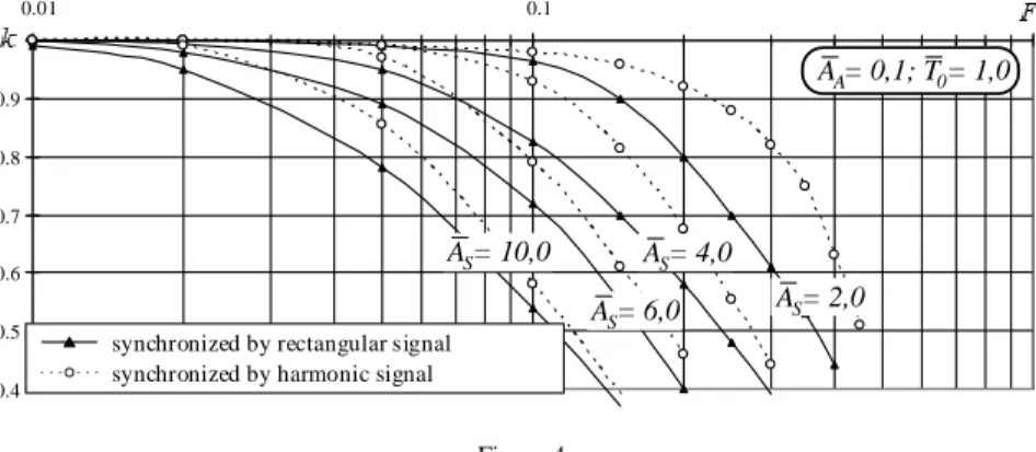
To determine the degree of dependence of the ISC dynamic characteristics on the parameters of the synchronizing signal 𝑋𝑆(𝑡), we applied MatLab + Simulink software to make the Bode magnitude plot 𝑘 = 𝑓(𝐹̅) of the integrating PLL system synchronized by both rectangular and harmonic signals with different values of synchronization depth (Fig. 4). An alternating harmonic signal 𝑋𝐴(𝑡) = 𝐴𝐴∙ 𝑠𝑖𝑛(2𝜋𝑓𝐴𝑡) with a constant amplitude 𝐴̅𝐴= |𝐴𝐴𝐴| = 0,1 and frequency 𝑓𝐴 was applied to the ISC input that was also exposed to the synchronizing effect 𝑋𝑆(𝑡).
The central component 𝑌0 of the ISC output pulses was isolated using a digital filter that implements the algorithm 𝑌0= 𝐴 ∙ (𝑡2− 𝑡1)/𝑇0. Here, 𝑡1, 𝑡2, 𝑇0are the time intervals and period of the ISC output pulses (Fig. 2c), and А is its amplitude.
In this case, the input signal level 𝑋𝐴(𝑡) and the average value 𝑌0 of the ISC output pulses get uniquely connected only after the repetition period 𝑇0 of the pulses 𝑌(𝑡) ends.
Fig. 4 uses the following notations: 𝑘 = 𝑌0.𝑚/𝐴𝐴 is the ISC transmission coefficient; 𝐹̅ = 𝑓𝐴/𝑓𝑆 is the scaled frequency of the harmonic signal 𝑋𝐴(𝑡) with respect to the frequency 𝑓𝑆 of the synchronizing effect 𝑋𝑆(𝑡).
0.4 0.5 0.6 0.7 0.8 0.9 1
0.01 0.1 1
synchronized by rectangular signal synchronized by harmonic signal
A = 10,0S
A = 6,0S A = 4,0S
A = 2,0S A = 0,1; T = 1,0A 0
Figure 4
Bode magnitude plot of the integrating PLL with different values of synchronization depth Analysis of the Bode magnitude plot (Fig. 4) allows us to conclude [17] that the integrating PLL’s dynamic properties are close to ones of the first-order aperiodic link 𝑊(𝑝) = 1 (𝑇⁄ 𝐸𝑝 + 1) with the time constants equivalent 𝑇𝐸≈ 0,25𝐴̅𝑆∙ 𝑇𝑆 (5) for synchronization by rectangle pulses and 𝑇𝐸≈ (𝜋 ∙ 𝐴̅𝑆∙ 𝑇𝑆) 16⁄ (6) for synchronization by harmonic signal.
However, it needs to be considered that this “linearization” is valid for only the 𝐹̅ = 𝑓𝐴/𝑓𝑆≤ 0,5 area of input frequency impact, which is derived from the Kotelnikov theorem [18]. If the frequency is higher, the scanning converter, being
a pulse system, switches to the slow sampling of dynamic input signal mode [13, 19].
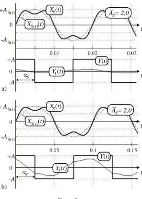
the integrating PLL is an adaptive filter whose parameters readjust into the functions of the amplitude 𝐴̅𝑆 and the frequency 𝑇𝑆−1 of the synchronization signal (of circuit voltage). As a result, the integrating PLL synchronizes with the circuit voltage with high accuracy (the synchronization angle error ∆𝛼̅𝑆 tends to zero) even if there are higher harmonics in the supply voltage and frequency instability of the synchronizing signal within the range of 50% and higher. This is confirmed by the results of the integrating PLL simulation when the synchronizing signal 𝑋𝑆(𝑡) has the third lowest-frequency voltage harmonic with the amplitude 𝐴̅𝑆(3)= 𝐴𝑆(3)/𝐴𝑆(1) that is equal to 30% of the main component amplitude 𝐴𝑆(1) of the circuit voltage with two frequency values 𝑓𝑆= 50 𝐻𝑧 (Fig.
5a) and 𝑓𝑆= 10 𝐻𝑧 (Fig. 5b) of the supply voltage.
0
0
0
0
t
t
t
t
0.01 0.02 0.03
0.05 0.1 0.15
A = 2,0S
A = 2,0S X (t)S(1)
Y(t) Y (t)I
Y (t)I
Y(t) X (t)S
X (t)S X (t)S(1) +AS(1)
-AS(1)
+A
-A +AS(1)
-AS(1)
+A
-A α S
α S b) a)
Figure 5
Waveform diagrams of the integrating PLL with the third harmonic in the synchronizing signal and the change in the supply voltage frequency: 𝑓𝑆= 50 𝐻𝑧 (a) and 𝑓𝑆= 10 𝐻𝑧 (b)
Fig. 5 shows that the 3rd harmonic is completely suppressed by the integrating PLL, and the synchronization angle S is equal to minus 90 el. deg. It is noteworthy that, other things being equal, a synchronization error occurs in the existing PLL systems (Fig. 1) because of the fixed values of the low-pass filter
bandpass and the PI-controller parameters that are tuned to the nominal frequency of the synchronizing voltage;
representation of the integrating PLL in the form of a first-order aperiodic filter indicates its high noise immunity to commutation and pulse distortions of circuit voltage. This is confirmed by the results of the integrating PLL system simulation when there are commutation notches in circuit voltage that reach the level of 𝛾𝐶 = 25 el. deg. (Fig. 6a). The notches were created by a three-phase bridge thyristor rectifier of current when it operated for a low-power circuit. In this case, the synchronization angle error was ∆𝛼̅𝑆= 0 (𝛼𝑆= −90 el. deg.), since commutation notches “1” and “2”, “3” and “4” mutually compensated each other in the time intervals t1 and t2, or areas 𝑆1′, 𝑆1′′ and 𝑆2′, 𝑆2′′ in subintervals 𝑡1′, 𝑡1′′ and 𝑡2′, 𝑡2′′ equal each other (Fig. 6b).
1
2 3
4
t
0 t 0
0.02 0.04 0.06 0.08
b) a)
A = 2,0S +AS
-AS
+A
-A
Figure 6
Waveform diagrams of the integrating PLL at commutation notches in circuit voltage (𝛾𝐶= 25 el. deg.)
In a real industrial environment the over-voltage amplitude and the circuit voltage frequency dips, generally, appear not instantly, but after a certain time interval, which depends on the loading conditions and the type of load included in the circuit. This is the reason why the analysis of the integrating PLL operation in the conditions of the smooth change in amplitude (Fig. 7a) and the frequency (Fig. 7b) of the circuit voltage appears to be of interest.
In Fig. 7 the following notations have been introduced: ∆𝐴̅𝑆 is the scaled error of an actual circuit voltage amplitude 𝐴𝑆 in relation to its rated value 𝐴𝑆.𝑁; 𝑆̅𝑈=
∆𝐴𝑆⁄𝐴𝑆.𝑁 is the scaled velocity of change in amplitude ∆𝐴𝑆 in one period 𝑇𝑆 of circuit voltage in relation to its rated amplitude 𝐴𝑆.𝑁; 𝑆 =(𝑇𝑆)−11𝑠𝑒𝑐−(𝑇𝑆.𝑁)−1 is the absolute velocity of change in the circuit voltage frequency (𝑇𝑆)−1 in the set time interval 𝑡3 equal to 1 second.
The results of the integrating PLL research have shown that in the dynamic operations the allowed velocity of change in amplitude 𝑆̅𝑈 in one circuit voltage period and the frequency 𝑆𝑓 makes 11 % and 9 Hz/s in 1 second in the conditions when the maximum synchronization angle inclination ∆𝛼𝑆 does not
transcend 2 el.deg., and the depth of synchronization is chosen out of the range 𝜋 2⁄ ≤ 𝐴̅𝑆≤ 8,0 (Fig. 8).
b)
0 1,0
t
“Soft” decrease
-1,0
AS.N
TS.N TS
t = 1s3
a)
0 t
“Soft” increase
“Soft” decrease 0,5
1,0 1,5
-0,5 -1,0 -1,5
AS.N
TS.N -ΔAS
ΔA = 0,5S ΔA = -0,5S
Figure 7
Test impact for analysis of the dynamic characteristics of the integrating PLL at the smooth changes of amplitude (a) and frequency (b) of the circuit voltage
-6 -4 -2 0 2 4 6 8
-0.5 -0.4 -0.3 -0.2 -0.1 0 0.1 0.2 0.3 0.4 0.5
0.25 1.0
2.0 4.0
8.0
a)
Δα , el.degS
S U
-6 -4 -2 0 2 4 6
-30 -25 -20 -15 -10 -5 0 5 10 15 20 25 30
8.0
1.0 0.5 4.0
b)
Δα , el.degS
S , Hz/secf
π/2
Figure 8
Graphs of dependencies of the absolute synchronization angle error ∆𝛼𝑆= 𝑓(∆𝑆̅𝑈) (a) and ∆𝛼 = 𝑓(𝑆𝑓) (b) for integrating PLL at different depth of synchronization ∆𝐴̅𝑆
The optimal level 𝐴̅𝑆 is considered to meet the range of 𝜋 2⁄ ≤ 𝐴̅𝑆≤ 4,0, when the speed of response and the immunity to noise are compromised.
The above results suggest the efficiency of using the integrating PLL in the control systems driven by SC and supplied by autonomous low-power supply systems with a high-level of distortion (higher harmonics and commutation notches) and unstable circuit voltage parameters as well.
Occurrence of the phase shift 𝛼𝑆 (equal to -90 el.deg) between the synchronization signal 𝑋𝑆(𝑡) and the output pulses 𝑌(𝑡) (Fig. 2b, c) of the integrating PLL (Fig.
2a) involves an untraditional set-up of the synchronization circuit of the SC control system (CS). One of the set-up options, for example, is the method of CS channel cross synchronization that can be applied in a three-phase thyristor rectifier with a synchronous multichannel control system (Fig. 9a).
Here the PLL-A output sync-pulse (with the duration of 180 el.deg.) outruns phase A by 90 el.deg. (Fig. 9b). Herein the rising flank of this pulse coincides with the natural commutation point of phase C. As a result, the synchronization of the phase C control channel can be done by the PLL-A output sync-pulse. The synchronization of other SC control channels can be done the same way (Fig. 9a).
In order to get the sync-pulses to coincide with the momentum of phase voltages going through the zero point, PLL-A, PLL-B and PLL-C should be synchronized from linear voltages AB, BC and CA, which outrun the phase ones А, В, С by 30 el.deg.
The integrating PLL (Fig. 2a) can be used in the control systems for active voltage (current) rectifiers, active power filters, matrix frequency converters and other SC.
These engineering solutions are considered in more detail in the paper [20].
b)
0 t
t t t 0
0 0
A B C A B C A B C
SU-A SU-B
SU-C α S(A)
α S(B) α S(C)
a)
PLL-A
PLL-B
PLL-C А B C
CS-A
CS-B
CS-C PSB
Figure 9
Block diagram (a) and the signal waveform diagram (b) of cross synchronization system of the semiconductor inverter (PLL-A, PLL-B, PLL-C – PLL of phase channels A, B, C; CS-A, CS-B, CS-C
– control system for phase channels A, B, C; PSB – power semiconductor block)
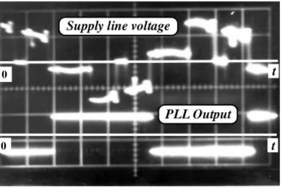
Fig. 10 shows the waveform chart of the circuit voltage and the output signal of the integrating PLL system, which functions in the cross-strapping mode (Fig. 9a) in the reverse thyristor rectifier for an electric drive of a direct current control system. The experiment took place on the diesel-generator plant of a drilling rig of the VI group. The total load of the plant was about 90%. Trouble-free performance of an entire technological complex was provided, despite the abnormally high-level of the circuit voltage distortion. This is achieved due to the ISC closed structure and an integrator in its direct control channel. With respect to the synchronizing effect, the system represents a first-order aperiodic filter with an equivalent time constant, which readjusts depending on the circuit voltage parameters.
Supply line voltage
PLL Output
0 0
t t
Figure 10
Waveform chart of the circuit voltage and the PLL system output signal in co-operation of several thyristor rectifiers for a low-power supply system
The PLL diagram, showed in Fig. 2a, was also tested on 84 AC thyristor regulators for the soft start of asynchronous electric drives [21] at the JSC
“Chelyabinsk Tube-Rolling Plant”, and showed high noise immunity and operational reliability.
Conclusions
An analysis of the static and dynamic characteristics of the integrating PLL, based on the integrating scanning conversion has been made. The PLL is a nonlinear impulse system based on the locked structure of an integrating scanning converter (SC) operating in the mode of external synchronization with circuit voltage frequency. It has been determined that for the SC the frequency of self-oscillation should be chosen equal to the scaled synchronization signal frequency. It excludes the drop out of outer synchronization mode of the device in the face of significant circuit voltage failures. At the frequency deviation of the supply voltage the equation listed above is satisfied due to the inclusion of the frequency correction block in the PLL system.
It has been shown that the integrating PLL system fully adapts to the instability of the amplitude and frequency of the circuit voltage within the range 50% and
higher. Unlike the existing PLL systems, the proposed system is a first-order aperiodic filter 𝑊(𝑝) = 1 (𝑇⁄ 𝐸𝑝 + 1) with the equivalent time constant 𝑇𝐸≈ (𝜋 ∙ 𝐴̅𝑆∙ 𝑇𝑆) 16⁄ and 𝑇𝐸≈ 0,25𝐴̅𝑆∙ 𝑇𝑆 for the harmonic synchronization signal and the rectangular one) that automatically adjusts depending on the amplitude and frequency of the circuit voltage. This property of the integrating PLL system allows suppressing higher harmonics in the power supply system, while frequency instability is within 50% and higher. Moreover, the proposed PLL system has high noise immunity to commutation distortions of the circuit voltage. This is achieved due to the closed SC structure and the presence of an integrator in its direct control channel.
Basing on the studies, we have formulated the recommendations on the choice of the integrating PLL system parameters. The optimal level of synchronization depth 𝐴̅𝑆 is the range 𝜋 2⁄ ≤ 𝐴̅𝑆≤ 4,0 where speed and noise immunity are compromised. In dynamic operating modes, the permissible change rate of the amplitude in one circuit voltage period is 11%, and that of the frequency per one second is 9 Hz/s, provided that the maximum deviation synchronization angle does not exceed 2 el. deg, and the synchronization depth is selected according to the condition 𝜋 2⁄ ≤ 𝐴̅𝑆≤ 8,0.
We have proposed a cross method for synchronizing the channels of SC control systems based on the integrating PLL. We have provided the results of the practical operation of the cross-strapping synchronization being a part of control systems of the reverse thyristor rectifier for a direct current electric drive and thyristor voltage regulator for soft start of asynchronous electric motors, which proved its high noise immunity and operation reliability.
Thus, we recommend that the proposed integrating PLL be used in SC control systems that are supplied by an autonomous low-power supply system with a high-level of distortions (higher harmonics and commutation notches) and unstable circuit voltage parameters.
Acknowledgement
The work was supported by Act 211 Government of the Russian Federation, contract № 02.A03.21.0011.
References
[1] Laszlo Tihanyi: Electromagnetic Compatibility in Power Electronics, Newnes, New York, 1995, 403 p.
[2] GOST 32144-2013. Electric energy. Electromagnetic compatibility of technical means. The quality norm of electric energy in general-purpose power supply systems, 2013
[3] Henry W. Ott: Noise reduction techniques in electronic systems, John Wiley & Sons, New York, 1988, 872 p.
[4] Marian P. Kazmierkowski, R. Krishman and Frede Blaabjerg: Control power electronics, Academic Press, USA, 2002, 518 p.
[5] M. M. Dudkin and L. I. Tsytovich: Adaptive integrators to control power valve converters, Russian Electrical Engineering, Vol. 86, No. 12, 2015, pp. 681-685
[6] J. Jacques, F. P. Dawson and R. Boriert: A tracking bandpass filter for the rejection of power system disturbances, EPE’9 35th European Conf. on Power Electronics and Applications, Vol. 4, No. 377, 1993, pp. 47-52 [7] Dan H. Wolaver: Phase locked loop circuit design, Prentice Hall, Inc.,
1991, 272 p.
[8] F. Liccardo, P. Marino and G. Raimondo: Robust and Fast Three-Phase PLL Tracking System, IEEE Transactions On Industrial Electronics, Vol.
58, No. 1, 2011, pp. 221-231
[9] P. Rodriguez, J. Pou, J. Bergas, J. I. Candela, R. P. Burgos and D.
Boroyevich: Decoupled Double Synchronous Reference Frame PLL for Power Converters Control, IEEE Transactions On Power Electronics, Vol.
22, No. 2, 2007, pp. 584-592
[10] В. К. Bose: Power Electronics and Variable Frequency Drives, IEEE Press, New York, 1996, 822 p.
[11] M. M. Dudkin, RF Patent 2,513,024, 2012.
[12] M. M. Dudkin, L. I. Tsytovich and A. S. Nesterov: Adaptive units and control systems of power semiconductor converters on the basis of integrating scanning conversion, Procedia Engineering, Vol. 129, 2015, pp.
933-939
[13] M. M. Dudkin, L. I. Tsytovich and O.G. Brylina: Spectral characteristics of scanning converters with pulse-width and pulse-frequency-width modulations, Russian Electrical Engineering, Vol. 84, No. 10, 2013, pp.
549-555
[14] L. I. Tsytovich, O. G. Brylina, M. M. Dudkin, R. M. Rakhmatulin and A.
V. Tyugaev: Analog-digital converter with integrating in-phase amplitude- frequency-pulse modulation for switched drive systems, Russian Electrical Engineering, Vol. 84, No. 10, 2013, pp. 244-249
[15] L. I. Tsytovich, M. M. Dudkin, O. G. Brylina and A. V. Tyugaev:
Integrating pulse-number ADC with high temporal and temperature stability of characteristics, Automatic Control and Computer Sciences, Vol.
49, No. 2, 2015, pp. 103-109
[16] L. I. Tsytovich, M. M. Dudkin, O. G. Brylina and A. V. Tyugaev:
Dynamics of communication lines with pulse-width and pulse-frequency-
width data carriers. Theory and practice, Russian Electrical Engineering, Vol. 85, No. 4, 2014, pp. 183-191
[17] L. I. Tsytovich, O. G. Brylina, M. M. Dudkin and R. M. Rakhmatulin:
Adaptive interval-code integrating synchronization of control systems for power converters, Russian Electrical Engineering, Vol. 84, No. 3, 2013, pp.
122-128
[18] C. Bissell: Vladimir Aleksandrovich Kotelnikov: Pioneer of the Sampling Theorem, Cryptography, Optimal Detection, Planetary Mapping ... History of Communications, Communications Magazine, IEEE, No. 10, 2009, рp.
24-32
[19] L. I. Tsytovich and M. M. Dudkin: Dynamics of scanning converters with sampling of instantaneous values of the control signal and various modulation patterns, Russian Electrical Engineering, Vol. 85, No. 10, 2014, pp. 619-627
[20] M. M. Dudkin: Energy-saving technologies in test stands with the use of single-phase reversible converters, Bulletin of SUSU. Series “Power engineering”, Vol. 13, No. 1, 2013, pp. 5-18
[21] M. M. Dudkin: Thyristor voltage regulator with adaptive integrating control system for smooth start-up of asynchronous electric motors, Bulletin of SUSU. Series “Power engineering”, Vol. 14, No. 2, 2014, pp.
36-43
[22] J. Dudrik and J. Oetter: High-Frequency Soft-Switching DC-DC Converters for Voltage and Current DC Power Sources, Acta Polytechnica Hungarica,Vol. 4, No. 2, 2007, pp. 29-46
[23] J-S. Guan et al.: Breast Tumor Computer-aided Diagnosis Using Self- Validation Cerebellar Model Neural Networks. Acta Polytechnica Hungarica, Vol. 13, No. 4, 2016, pp. 39-52
[24] R.-E. Precup, S. Preitl: PI-Fuzzy Controllers for Integral Plants to Ensure Robust Stability, Journal Information Sciences, Vol. 177, 2007, pp. 4410- 4429
[25] F. Tahri, A. Tahri, A. Allali and S. Flazi: The Digital Self-Tuning Control of Step a Down DC-DC Converter, Acta Polytechnica Hungarica,Vol. 9, No. 6, 2012, pp. 49-64
[26] H. K. Lam, F. H. F. Leung and P. K. S. Tam: Stable and Robust Fuzzy Control for Uncertain Nonlinear Systems, IEEE Transactions on Systems, Man and Cybernetics, Part A: Systems and Humans, Vol. 30, No. 6, 2000, pp. 825-840