Plasmon-plasmon coupling probed by ultrafast, strong-field photoemission with <7 Å sensitivity
Judit Budai, † a,b Zsuzsanna Pápa, † a,c István Márton,c Piotr Wróbel,d Tomasz Stefaniuk,d Zsuzsanna Márton,a,e Péter Ráczc and Péter Dombi*a,c
a ELI-ALPS Research Institute, ELI-HU Non-Profit Ltd., 6720 Szeged, Hungary.
b Department of Optics and Quantum Electronics, University of Szeged, 6720 Szeged, Hungary.
c MTA "Lendület" Ultrafast Nanooptics Group, Wigner Research Centre for Physics, 1121 Budapest, Hungary
d Faculty of Physics, University of Warsaw, 02-093 Warsaw, Poland
e Department of Experimental Physics, University of Pécs, 7624 Pécs, Hungary.
† Equal contributions.
Abstract
The coupling of propagating surface plasmon waves and localized plasmon oscillations in nanostructures is an essential phenomenon determining electromagnetic field enhancement on the nanoscale. Here, we use our recently developed ultrafast photoemission near-field probing technique to investigate the fundamental question of plasmon-plasmon coupling and its effect on large field enhancement factors. By measuring and analyzing plasmon field enhancement values at different nanostructured surfaces, we can separate contributions from propagating and localized plasmons.
When resonance conditions are met, a significant field enhancement factor can be attributed to the generation of localized plasmons on surface nanostructures, acting as dipole sources resonantly driven by the propagating plasmon field. Our plasmon-plasmon coupling results can contribute directly to applications in surface enhanced Raman scattering (SERS), the development of plasmonic sensors and nanostructured photocathodes.
Introduction
Nanoscale electromagnetic field localization in the closest proximity of metal nanostructures is a phenomenon exploited in many important applications. Field nanolocalization can either have a geometric origin rooted in the nanometer-scale radius-of-curvature of surface features. This phenomenon inherently goes together with the enhancement of the incoming (laser) field at the sharpest features and it is well studied with metal nanotips. Field enhancement factors of up to ×10 can be achieved this way for direct optical excitation1-5 (even without plasmon coupling). A more promising path toward large field enhancement is the generation of surface plasmons in various environments. Both propagating surface plasmon waves at metal films or localized plasmon oscillations in metal nanoparticles are suitable tools to achieve substantial field enhancement6,7. This field enhancement represents the basis for many important applications such as the development of templates used for surface enhanced Raman scattering (SERS)8-10, plasmonic biosensors11,12 also for single molecule detection13 and many more14-17.
Electromagnetic coupling phenomena represent essential ingredients for tailoring plasmonic systems and devices. In addition to well-known light-plasmon and plasmon-light coupling (scattering) processes, coupling between propagating and localized surface plasmon modes can occur on suitable samples strongly affecting the achievable maximum field enhancement. Signatures of plasmon- plasmon coupling can be indirectly investigated with optical spectroscopy methods18,19. More direct information on this type of coupling can be gained with scanning probe tools20,21 and photoelectron
emission microscopy22,23. However, these approaches all have in common that they lack information on the absolute value of nanoplasmonic field enhancement. In a more general context, there are other methods for determining field enhancement like surface enhanced Raman-scattering24, two-photon photopolymerization25, two-photon photoluminescence26, nano-ablation27, measurement of DC photocurrent in plasmonic gaps28 or determination of the Purcell-factor29. Although these provide a sound estimate for field enhancement they were not used for studying plasmon-plasmon coupling.
Since the coupling effect plays a key role in efficiency of plasmon-based devices, for proper plasmonic device engineering, one requires a direct and independent feedback both on the magnitude and sources of plasmon field enhancement with the most relevant coupling phenomena considered. This need is satisfied by our recently demonstrated method30 which offers a way to establish the field enhancement factor for any nanostructured metal samples based on ultrafast photoemission from metal nanostructures.
Here, we apply this method for the first time to investigate the coupling of propagating surface plasmon waves and localized plasmon oscillations. We show that the method provides an ultrahigh,
<7 Å measurement sensitivity of the plasmon near-field at the metal surface enabling us to exactly determine the contributions of both localized and propagating plasmons, keeping in mind that the former decays within only a few nanometers distance from the sample surface.
Results and discussion
Retrieving plasmon field enhancement
We achieve different degrees of plasmon-plasmon coupling by fabricating three different plasmonic thin films (supporting propagating plasmons) with highly controlled, varying surface roughness. Typical surface nanostructures with different sizes on each sample support localized plasmon oscillations.
Here, we set out to measure field enhancement contributions originating from propagating and from localized surface plasmons on each nanostructured sample.
Our field enhancement measurement method is based on the observation that if photoelectrons are emitted at a favorable phase of the electric field, after roughly a half optical cycle they can return to the metal surface and elastically rescatter there, boosting their kinetic energy (Qmax) until up to 10 times the ponderomotive energy according to
Qmax = (10.01e22Eloc,max2) / (162mc2) + 0.54W
Here e and m are the electron charge and mass, respectively, λ is the laser wavelength, Eloc is the local electromagnetic field, c is the speed of light and W is the work function of the metal. Explanation of the numerical prefactors can be found in Refs. 31 and 32. The rescattering process is in complete analogy with above threshold ionization of atoms33. Here, by measuring plasmonic photoelectron spectral cutoffs experimentally, we can simply deduce the maximum near-field enhancement value on a given sample illuminated by femtosecond laser pulses.
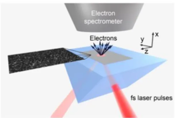
Fig. 1 Measurement scheme for the investigation of plasmon-plasmon coupling probed by photoelectron spectroscopy. Plasmons are generated on surfaces with precisely controlled roughness by femtosecond laser pulses to achieve sufficient intensity for the photoacceleration of the electrons in nanooptical near-fields.
The measurement setup based on this concept is illustrated in Fig. 1. We use femtosecond laser pulses with 38-fs pulse length, 795 nm central wavelength and 1 kHz repetition rate to generate propagating surface plasmon waves by focusing them onto a 50 nm-thin Ag film evaporated onto the superpolished face of a right-angle fused silica prism. Most importantly, by precisely controlling the temperature during electron beam evaporation process and applying different wetting layers (Ni, Ge and no wetting layer 34-36), we could achieve highly controlled thin films with exhibiting 0.8 nm, 1.6 nm and 4.5 nm root-mean-square (rms) surface roughness with a certain distribution of Ag surface nanostructures.
The left column in Fig. 2 shows atomic force microscope (AFM) images of the surfaces after applying tip shape deconvolution. In order to gain maximum field enhancement on each sample, we acquired plasmonic photoelectron spectra using a time-of-flight electron spectrometer at different laser intensities at the resonant angle of incidence (measured beforehand).
Fig. 2 Surface morphology and the corresponding electron spectra. (a-c) Atomic force microscope scans of plasmonic surfaces with controlled, different rms roughnesses of 0.8 nm, 1.6 nm and 4.5 nm, after applying a tip shape deconvolution procedure. (d-f) Plasmonic photoelectron spectra (logarithmic scale) from the three surfaces by generating plasmons with a 38-fs laser pulse with different focused intensities. Black symbols correspond to electron spectral cutoffs. Cutoff error bars are determined according to fit uncertainty.
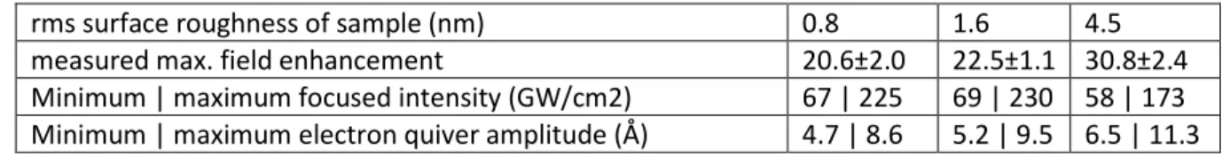
It can be seen in Fig. 2 that for each sample, energy cutoffs scale linearly with intensity, evidencing the ponderomotive nature of the generation of the most energetic electrons. By evaluating cutoffs according to (1), maximum field enhancement for each surface was assessed, yielding 20.6±2.0, 22.5±1.1 and 30.8±2.4 for surfaces with 0.8 nm, 1.6 nm and 4.5 nm rms roughness, respectively.
Our near-field probing method has the remarkable feature that it has an ultrahigh sensitivity with the photoelectrons probing the maximum local fields in a 5-7 Å thin surface layer. This is evidenced by the quiver amplitude of the electrons in the local fields. This oscillation amplitude is given by1 A = eEloc 2 / (4 2mc2), therefore, one can tabulate these amplitudes for each surface and for each laser intensity value. Electrons contributing to spectral cutoffs perform a half-cycle quiver motion before rescattering17, as such, our near-field probe is sensitive in an ultrathin surface layer with a thickness comparable to the quiver amplitude. Tabulated quiver amplitudes in Table 1 for each of our samples evidence that for the lower laser intensity range, field enhancement can be measured in a layer with some 5-7 Å thickness at the surface that we probe. This is an unparalleled feature of our photoelectron probe.
Table 1. Comparison of maximum field enhancement and plasmon-field decay values for the 3 test surfaces with different roughness.
rms surface roughness of sample (nm) 0.8 1.6 4.5
measured max. field enhancement 20.6±2.0 22.5±1.1 30.8±2.4
Minimum | maximum focused intensity (GW/cm2) 67 | 225 69 | 230 58 | 173 Minimum | maximum electron quiver amplitude (Å) 4.7 | 8.6 5.2 | 9.5 6.5 | 11.3
Contributions of localized and propagating plasmons
Most remarkably, our measurements show that there is a non-trivial relationship between the experimental field enhancement values and the surface roughness of the samples. The unexpected and significant increase of the field enhancement for the probe with the roughest surface requires further analysis of the electromagnetic phenomena on these samples. To analyze this relationship, the coupling of propagating and localized plasmon modes has to be considered. In order to separate field enhancement contributions from both types of plasmons, we performed numerical simulation of the plasmon excitation and plasmon-plasmon coupling processes.
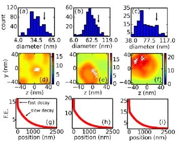
Fig. 3 Simulation of field amplitudes. (a-c) Surface nanostructure size distribution of the Ag surfaces with rms roughness of 0.8 nm, 1.6 nm and 4.5 nm, respectively. Arrows indicate surface nanostructure sizes for which field distributions are presented in (d-f) by simulating AFM-scanned surface elements.
White crosses show the location of the hottest spots, where the corresponding decay curves were averaged. These averaged curves are plotted along the surface normal in (g-i). (g-i) Simulated field amplitude profiles with a clearly visible two-component decay.
In order to determine that electrons from which surface nanostructures contribute to the observed spectral cutoffs, we considered the actual surface nanostructure size distribution on each nanostructured surface (Figs. 3(a-c)). Field enhancement values near the surface of the nanostructures were gained by evaluating field distribution maps (see Figs. 3(d-f) representing typical surface nanostructures). Our simulations revealed that within the 20 nm - 90 nm surface nanostructure size range the field enhancement continues to grow due to localized plasmon resonance (Fig. 4.). Since the surface nanostructures which are still represented considerably in the size distribution, are smaller than 90 nm, we chose the largest surface nanostructure from each sample which is represented with at least half of the maximum value of each distribution (Figs. 3(a-c)). This way, we simulated typical surface nanostructures for each surface that provide a measurable photoemission electron signal contributing to the cutoff electrons.
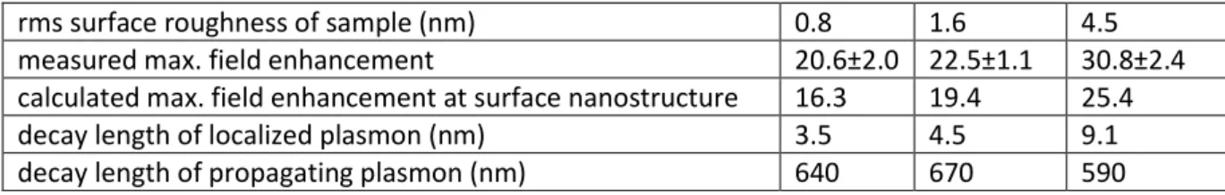
For the smoothest surface, typical, AFM-scanned surface nanostructures of ~50 nm diameter give a maximum simulated field enhancement value of ×16.3, see Fig. 3(d). We analyzed the situation further by plotting the field amplitude (in units of the amplitude of the incoming field) along surface normals taken at the hottest spots of each surface nanostructure (white crosses in Fig. 3(d-f)). Averaging these lineouts reveals the simultaneous presence of propagating and localized plasmons since two decay lengths are clearly visible: one sharp component corresponding to localized plasmons with 3.5 nm 1/e decay length and a shallow decay with 640 nm length corresponding to propagating plasmons. We deduced the field enhancement contribution of localized and propagating plasmons with the steps detailed in the methods section and we found that the propagating plasmon component accounts for most of the field enhancement (×12.1).If the same procedure is applied to typical surface nanostructures of the two other surfaces with 1.6 nm and 4.5 nm roughness, maximum field enhancement values of ×19.4 and ×25.4 are revealed for typical hot-spot surface nanostructures with
~65 and ~90 nm diameter. The corresponding decay components are characteristically similar as above, summarized in Table 2.
Table 2. Comparison of maximum field enhancement and plasmon-field decay values for the 3 test surfaces with different roughness.
rms surface roughness of sample (nm) 0.8 1.6 4.5
measured max. field enhancement 20.6±2.0 22.5±1.1 30.8±2.4
calculated max. field enhancement at surface nanostructure 16.3 19.4 25.4
decay length of localized plasmon (nm) 3.5 4.5 9.1
decay length of propagating plasmon (nm) 640 670 590
Measured and simulated field enhancement values correspond well to one another with a slight systematic numerical underestimation. In general, our results show the enhanced generation of localized plasmons for the roughest surface and moderate field enhancement for the other two surfaces. This prompts us to conclude that the highest field enhancement can be achieved for a surface where propagating plasmons can couple strongly to localized plasmons on surface nanostructures.
To support this claim, we computed and plotted field enhancement on several surface nanostructures as a function of nanostructure size in Fig. 4. This shows the contribution of the localized plasmon component in the overall field enhancement (by subtracting the propagating plasmon component, c.
f. Fig. 6 in methods section). The field enhancement continues to grow in the 20 nm - 90 nm surface nanostructure size range, where it saturates due to localized plasmon resonance, showing that the coupling is more efficient at larger surface nanostructures, also evidenced by our experiments.
Fig. 4 Resonance behavior of field enhancement contribution of localized plasmons and surface charge density. Field enhancement contribution of localized plasmons on surface nanostructures to the total field enhancement as a function of nanostructure size. Black data points correspond to simulations of actual, AFM-scanned surface nanostructures with different diameters, with the black curve illustrating the resonance-like behavior. Maximum field enhancement was computed for different surface nanostructures and the propagating plasmon contribution was subtracted. Error bars represent standard AFM resolution (±5 nm for 10 nm radius-of-curvature of the tip). The dashed blue-green curve show results (evaluated the same way) on hypothetical samples with a single semi-ellipsoid positioned on an atomically flat silver film. In addition to field enhancement resonance, surface charge density resonance is also plotted for these samples (dashed grey curve).
The fundamental nature of the plasmon-plasmon coupling resonance in Fig. 4 is also illustrated by simulations of a hypothetical sample containing a single semi-ellipsoidal nanostructure lying on an atomically smooth plasmonic silver layer. By separating the localized plasmon contribution to the overall field enhancement in the same way, a similar plasmon-plasmon coupling resonance is
observed, peaking at around 75 nm surface nanostructure diameter (blue-green curve in Fig. 4). Our simulations enable the determination of the surface charge density distributions, as well. This provides a more fundamental representation of the coupling mechanism since localization takes place due to the presence of resonantly driven surface charges at surface nanostructures with favorable size. As expected, the maximum surface charge density values also show surface nanostructure size dependence and the resonance behavior is well visible (Fig. 4).
Coupling mechanism
Thus, the physical background of the observed phenomena can be summarized as follows: ultrashort laser pulses launch propagating plasmonic wavepackets on the silver film. If these waves reach a metallic surface nanostructure with a suitable geometry, they can resonantly drive dipole-like oscillations localized to the surface nanostructure, yielding an increased field enhancement factor at the surface nanostructure. The observed (experimentally measured) extra field enhancement evidences the plasmon-plasmon coupling phenomenon.
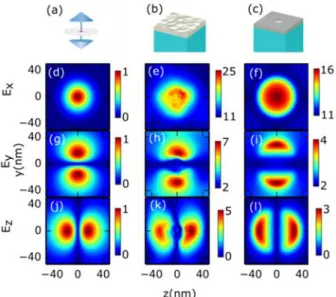
In order to provide further confirmation of this picture, we computed field distribution maps (i) for a dipole, oscillating along the x-direction, (ii) an AFM-scanned ~65 nm-diameter plasmonic surface nanostructure and (iii) an artificial semi-ellipsoidal surface nanostructure with 65 nm diameter. We compared maps for the Ex, Ey and Ez components of the field amplitude for cases (i-iii) in a plane positioned 2 nm above the top of the surface nanostructure (see Fig. 5). The difference between cases (i) and (iii) can be attributed to the fact that (i) is a point source whereas for (iii) we computed fields for an extended nanoparticle. The good correspondence between the dipole fields and optical near- fields in Fig. 5 (both for the AFM-scanned surface nanostructure and for the artificial surface nanostructure) evidences that plasmons propagating along the y-axis drive dipole-like charge oscillation on resonant surface nanostructures. Their field is superimposed to that of the propagating wave, shown by the color-scale offsets in Figs 5(e), (f), (h) and (i). This, together with the good agreement between measured and simulated enhancement values, indicates that plasmon-plasmon coupling is well accounted for by the ultrafast photoelectron probing method.
Fig. 5 Dipole-like behavior of surface nanostructures. Scheme of (a) a modeled dipole, (b) modeled rough silver surface (rms roughness 4.5 nm) with a ~65-nm-diameter surface nanostructure in the centre and (c) silver surface with a semi-ellipsoid (diameter: 65 nm, height: 6.5 nm). (d), (g) and (j)
Normalized field distribution maps for x, y and z-components of the electric field of a dipole being parallel to the x-axis. (e), (h) and (k) Field distribution maps in a plane 2 nm above a 65-nm-diameter surface nanostructure on the Ag layer with 4.5 rms roughness. (f), (i) and (l) Field distribution maps in a plane 2 nm above a 65-nm-diameter surface nanostructure on a smooth Ag layer. The color bars are offset in (e), (f), (h) and (i) to indicate only the dipole component, the residual background in the Ex and Ey field amplitude components can be attributed to the presence of propagating plasmons on the surface. They propagate along the y-axis and have 0 electric field component in the z-direction, as expected.
Conclusions
In summary, we probed field enhancement attributed to plasmon-plasmon coupling with a recently demonstrated, ultrafast experimental method. Ultrasensitive near-field probing revealed maximum field enhancement factors between ×20 and ×31 for silver surfaces with controlled roughness. The coupling of localized plasmons to propagating ones results in a distinctive resonance phenomenon on
~95 nm diameter surface nanostructures providing a sudden increase of the measured field enhancement from a factor of ~20 to ~30. Simulation results corresponded well to measured maximum field enhancement values and this way, the field enhancement contribution provided by the localization of propagating plasmons on surface nanostructures could be clearly identified, amounting to ~50% of the total field enhancement at samples where strong plasmon-plasmon coupling is realized.
These experiments open a pathway not only toward the investigation of plasmon coupling processes, but also toward better exploitation of these phenomena in real-world environments and engineering of plasmonic samples with experimental field enhancement feedback. In the future, nanostructured surfaces can be directly optimized for plasmonic field enhancement in applications where this is crucial, such as single-molecule spectroscopy and SERS8-10,13,37, plasmonic sensors11,12, switches38-40 and nanostructured photocathodes41-45. Plasmon field probing with ultrafast photoemission provides relevant physical insight into the emergence of electromagnetic field enhancement; it is suitable for time-resolved measurements4,46,47 and as such, it is expected to lead to better nanofabrication and further discoveries in the field of ultrafast plasmonics.
Methods
Experimental setup
38-fs pulses were delivered by a regenerative Ti:sapphire amplifier (“Legend Elite” from Coherent Inc., 1 kHz repetition rate at 795 nm central wavelength). Electrons emitted from the plasmonic samples were collected by a time-of-flight (TOF) spectrometer (designed and built by Kaesdorf GmbH with a flight tube of 45 cm length, acceptance angle 37°). The Kretschmann-prism acted as the vacuum window of the TOF chamber with the thin film samples being on the vacuum side. The axis of the flight tube of the TOF spectrometer is normal to the surface of the sample where the plasmonic thin film is situated (see Fig. 1.). Electron counts from a microchannel plate detector at the end of the magnetically shielded flight tube were recorded by a fast multiscaler card (100 ps time resolution). The discrimination level for these signal pulses was set to 4 mV. After calibration, electrons having kinetic energies in the 3 eV to 100 eV range could be accurately measured with this setup.
Plasmonic samples
Sample preparation Silver thin film samples were produced by electron beam evaporation of Ag. By precisely controlling the temperature during the electron beam evaporation process and applying different wetting layers (Ni, Ge and no wetting layer34-36), we could achieve thin films with 0.8 nm, 1.6 nm and 4.5 nm root-mean-square (rms) surface roughness with a well-controllable distribution of Ag surface nanostructures.
Surface characterization AFM measurements under tapping mode in air were carried out utilizing an Ntegra NTMDT microscope equipped with sharp etalon probes with a 10 nm tip curvature radius. The resonant frequency of the probes is equal to 140 kHz, which corresponds to a force constant of 3.5 N/m. The averaged RMS value was measured on several areas of the samples. Tip shape deconvolution procedure was carried out supposing a typical tip shape (cone opening angle of 30 degrees on the last 200 nm of the shank).
Simulations
For modeling the measured samples, representative areas with 300 nm × 300 nm lateral size were chosen from deconvoluted AFM images. We used a finite-difference time-domain approach to model the test surfaces (FDTD Solutions / Lumerical Inc.) 50 nm silver layer thickness was set. Refractive index of fused silica was described with constant n = 1.45. We used optical constants of silver that were measured on samples deposited under the same conditions as our samples under study34,35. This way, the effect of the inner structure (polycrystalline nature) of the layers is taken into account phenomenologically. First, we checked the optimum excitation angles in the model by looking for the angular reflection minimum in the Kretschmann-type illumination geometry. These angles from simulations are 44.5°, 44.6° and 44.9° for the surfaces with increasing roughness, being in good accordance with the experimental observations, yielding 44.5°, 44.5° and 44.9° for the same values, respectively. The presented results were calculated at resonant angles of incidence with a 3D non- uniform mesh with step sizes between 0.25 and 0.5 nm near the surface region. The field distributions were recorded by 3D frequency domain field and power monitors, while the surface charge density distributions were deduced from time monitor data. The same simulation conditions were applied for the artificial semi-ellipsoids. The FDTD simulation parameters given above were set according to a strict convergence check.
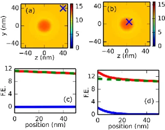
Separation of localized and propagating plasmon fields For calculating the field enhancement contribution of localized and propagating plasmons we plotted the field amplitude along surface normals taken at the hottest spots of each surface nanostructure and averaged these lineouts. Field contributions of the propagating plasmons were calculated by fitting an exponentially decaying curve to a section of the averaged curve with a distance between 50 nm and 1000 nm from the edge of the surface structure since the localized plasmons affects the field amplitude only within a much shorter distance from the surface. By subtracting the contribution of propagating plasmons gained this way from the overall field amplitude, we can determine the rapid decay of localized plasmons.
Fig. 6 shows this process for two cases. When the decay is studied on a perfectly smooth surface element far from the semi-ellipsoid, we observe an exponential decay consisting only one exponential term, since far from the structure there is no localization and only the propagating plasmons contribute to the field. When we are on the surface structure supporting field localization, the decay curve can not be represented with a single exponential term anymore, therefore, we have to introduce an
additional, rapidly decaying exponential term which is attributed to the localized plasmon contribution to the field decay curve.
Fig 6 (a) and (b) Field distribution maps computed for an artificial semi-ellipsoid lying on a perfectly smooth silver layer. Blue crosses indicate the positions where the field amplitude lineouts were taken which are plotted in (c) and (d) along the surface normal. In (c) and (d) red lines show the overall field amplitude, blue curves represent the contribution of localized plasmon components while dashed green ones correspond to propagating plasmons. Note that for (c) red and green curves overlap indicating that by moving away laterally far from the surface structure, the field component associated with plasmon localization on the surface nanostructure disappears.
Conflicts of interest
There are no conflicts of interest to declare.
Acknowledgements
We would like to thank N. Kroó and J. Krenn for fruitful discussions as well as the Ultrafast Nanooptics Group at the University of Oldenburg for providing CPU time to run simulations. P. Rácz received a Bolyai Research Scholarship of the Hungarian Academy of Sciences (MTA). The authors acknowledge the Hungarian Academy of Sciences (“Lendület” Grant, Ultrafast Nanooptics) and the National Research, Development and Innovation Office of Hungary (projects 109257 and VEKOP-2.3.2-16-2017- 00015). We also acknowledge the Max Planck Society for support in the form of a Partner Group Grant.
References
1 G. Herink, D. R. Solli, M. Gulde and C. Ropers, Nature, 2012, 483, 190.
2 B. Piglosiewicz et al., Nature Phot., 2014, 8, 37.
3 S. Thomas, M. Krüger, M. Förster, M. Schenk and P. Hommelhoff, Nano Lett., 2013, 13, 4790.
4 K. Echternkamp et al., Appl. Phys. B, 2016, 122, 80.
5 S. Thomas et al. New J. Phys., 2015, 17, 063010.
6 H. A. Atwater, Sci. Am., 2007, 296, 56.
7 J. A. Schuller et al., Nat. Mater., 2010, 9, 193.
8 A. Campion and P. Kambhampati, Chem. Soc. Rev., 1998, 27, 241.
9 K. A. Willets and R. P. Van Duyne, Annu. Rev. Phys. Chem., 2007, 58, 267.
10 Y. Liu, S. Xu, H. Li, X. Jian, and W. Xu, Chem. Comm., 2011, 47, 3784.
11 J. N. Anker et al., Nat. Mater., 2008, 7, 442.
12 J. Homola, Chem. Rev., 2008, 108, 462.
13 P. Zijlstra, P. M. R. Paulo and M. Orrit, Nat. Nanotechnol., 2012, 7, 379.
14 M. I. Stockman, Opt. Express, 2011, 19, 22029.
15 B. Ahn et al., Opt. Express, 2016, 24, 92.
16 B. Ahn et al., APL Photonics, 2017, 2, 036104.
17 P. Dombi et al., Nano Lett., 2013, 13, 674.
18 Y. Chu and K. B. Crozier, Opt. Lett., 2009, 34, 244.
19 A. Hohenau and J. R. Krenn, Phys. Stat. Sol. Rapid Res. Lett., 2010, 4, 256.
20 S. I. Bozhevolnyi, B. Vohnsen, I. I. Smolyaninov and A. V. Zayats, Opt. Comm., 1995, 117, 417.
21 S. I. Bozhevolnyi, V. Volkov and K. Leosson, Phys. Rev. Lett., 2002, 89, 186801.
22 A. Kubo et al., Nano Lett., 2005, 5, 1123.
23 C. Lemke et al., Nano Lett., 2014, 14, 2431.
24 Y. Fang, N.-H. Seong, D. D. Dlott, Science, 2008, 321, 388.
25 C. Deeb et al., ACS Nano, 2010, 4, 4579.
26 P. J. Schuck, D. P. Fromm, A. Sundaramurthy, G. S. Kino, W. E. Moerner, Phys. Rev. Lett., 2005, 94, 017402.
27 R. K. Harrison, A. Ben-Yakar, Opt. Express, 2010, 18, 22556.
28 D. R. Ward, F. Hüser, F. Pauly, J. C. Cuevas, D. Natelson, Nat. Nanotechnol. 2010, 5, 732.
29 S. A. Maier, Opt. Exp., 2006, 14, 1957.
30 P. Rácz et al., Nano Lett., 2017, 17, 1181.
31 M. Busuladžić, A. Gazibegović-Busuladžić and D. Milošević, Laser Phys., 2006, 16, 289.
32 M. Krüger et al., New J. Phys., 2012, 14, 085019.
33 G. G. Paulus, W. Nicklich, H. Xu P. Lambropoulos and H. Walther, Phys. Rev. Lett., 1994, 72, 2851.
34 T. Stefaniuk, P. Wróbel, P. Trautman and T. Szoplik, Appl. Opt., 2014, 53, 237.
35 P. Wróbel et al., ACS Appl. Mater. Interfaces, 2015, 7, 8999.
36 A. Ciesielski, L. Skowronski, M. Trzcinski and T. Szoplik, Appl. Surf. Sci., 2017, 421B, 349.
37 K. Kneipp, H. Kneipp, I. Itzkan, R. R. Dasari and M. S. Feld, Chem. Rev., 1999, 99, 2957.
38 J. Chen, Z. Li, X. Zhang, J. Xiao and Q. Gong, Scientific Reports, 2013, 3, 145.
39 T. Higuchi, L. Maisenbacher, A. Liehl, P. Dombi and P. Hommelhoff, Appl. Phys. Lett., 2015, 106, 051109.
40 K. Wang et al., Appl. Phys. Lett., 2017, 111, 181102.
41 R. K. Li et al., Phys. Rev. Lett., 2013, 110, 074801.
42 M. Swanwick et al., Nano Lett., 2014, 14, 5035.
43 A. Polyakov et al., Phys. Rev. Lett., 2013, 110, 076802.
44 R. G. Hobbs et al., ACS Nano, 2014, 8, 11474.
45 K. Appavoo et al., Nano Lett., 2014, 14, 1127.
46 P. Dombi et al. Opt. Express, 2010, 18, 24206.
P. Földi, I. Márton, N. Német, V. Ayadi and P. Dombi, Appl. Phys. Lett., 2015, 106, 013111.