Contents lists available atScienceDirect
Applied Surface Science
journal homepage:www.elsevier.com/locate/apsusc
Complementary physicochemical analysis by ellipsometry and Auger spectroscopy of nano-sized protective coating layers
Peter Petrik
⁎, Adel Sarolta Racz, Miklos Menyhard
Institute of Technical Physics and Materials Science, Centre for Energy Research, Konkoly-Thege Rd. 29-33, 1121 Budapest, Hungary
A R T I C L E I N F O Keywords:
Ion mixing Optical properties Spectroscopic ellipsometry Auger electron spectroscopy Silicon carbide
Protective layer Depth profiling Physicochemical analysis
A B S T R A C T
Protective SiC-rich nano layer was created by ion beam mixing of Si/C multilayers. The transformation of the Si and C layers into a homogeneous SiC layer was analyzed using complementary depth profiling by spectroscopic ellipsometry (SE) and Auger electron spectroscopy (AES). The distribution of elements and their chemical states was revealed by AES, whereas SE measured the accurate thicknesses, density, crystallinity, and the distribution of different phases. The optical properties of the created SiC layer determined by SE were almost identical to that of ion implantation-amorphized SiC. Amorphous Si and void formations were revealed by SE. The void profile determined by SE correlated well with the Xe distribution measured by AES. The complementary capabilities of SE and AES for a detailed chemical investigation were pointed out, such as the atomic (AES), structural (AES and SE) and non-destructive depth profiling (SE) features. It was shown that besides the synergism that the two methods reveal, SE is capable of a quick, sensitive and non-destructive testing of such layer structures and materials.
1. Introduction
There is an increasing demand for devices based on nano layers for various applications [1,2]. These devices might work in harsh en- vironments (e.g., in automotive and aerospace applications such as combustion processes, gas turbine control, oil industry, etc.). For stable operation, they are to be protected against chemical and mechanical attacks, which can be done by various protective layers[3]. Those films used in harsh environments are usually made from extremely stable compounds resistant against chemical and mechanical attacks [4–6].
These compounds are usually of high heat of formation ones and made in usual circumstances at elevated temperatures. If one intends to protect a device made of nanosized layers, the application of high temperature for making the protection layer is generally not allowed, since it might destroy the device itself. For these cases, for the pro- duction of the protective layer, such methods are applied that use non- equilibrium type conditions, where the application of high temperature is not necessary. One of these methods is the ion bombardment-induced mixing[7].
As an example, we have studied the production of a silicon carbide (SiC)-rich nano layer by ion irradiation of thin C and Si layers[8]. SiC is a material of high-temperature strength, thermal shock resistance, good thermal conductivity and its inertness when exposed to corrosive en- vironments[9–13]. There are different methods to produce SiC thin
layers like chemical vapor deposition (CVD) and physical vapor de- position (PVD)[12,14]. Laboriante et al. deposited 50 nm thick SiC on Si (100) at 780 °C applying low pressure CVD[13]. Daves et al. de- posited 250 nm thick SiC thin films at 400 °C applying plasma enhanced CVD[15]. Xu et al. used RF plasma sputtering and a compound SiC target to deposit SiC nanoparticles on Si(100) substrates at the sub- strate temperature of 350 °C[16]. Chung et al. have shown the for- mation of SiC nanoparticles (NPs) from Si/C/Si multilayer using thermal annealing at 700–900 °C[17]. The size and density of SiC NPs were strongly influenced by the thickness of Si, the number of the layers and the annealing temperature. In the cited works elevated temperature had to be applied to obtain a layer of sufficient quality[18].
We have shown that applying noble gas ion bombardment in the range of 40–120 keV on a properly chosen Si/C multilayer system, SiC- rich layer of desired thickness can be formed at room temperature and the layer exhibits superior resistance against chemical and mechanical attacks [19–21]. The layers were characterized by Auger electron spectroscopy (AES) depth profiling. AES is sensitive to the chemical state of the elements since the Auger peak shapes and energies might change due to the compound formation. E.g. the AES can easily dis- tinguish between carbon in form of graphite or carbide. The depth profiling provides the in-depth distribution of the constituents (ele- ments and compounds separately), which can be correlated with the features of the layer. On the other hand, AES fails to show the
https://doi.org/10.1016/j.apsusc.2020.147593
Received 17 April 2020; Received in revised form 15 August 2020; Accepted 16 August 2020
⁎Corresponding author.
E-mail address:petrik@mfa.kfki.hu(P. Petrik).
Available online 19 August 2020
0169-4332/ © 2020 The Authors. Published by Elsevier B.V. This is an open access article under the CC BY license (http://creativecommons.org/licenses/by/4.0/).
crystalline state of the materials, the possible defects (e.g. vacancies), and the thickness scale accuracy is poor. Luckily, spectroscopic ellip- sometry (SE) provides this complementary information: (i) it is capable of a reference-free thickness determination with sub-nanometer sensi- tivity, and therefore it can be used as a thickness calibration for the AES; (ii) it can measure the optical (and physical) density of the layer;
(iii) it is very sensitive to the crystallinity, the long-range order in the material. We will show the synergism of the simultaneous application of AES and SE, two high-sensitivity methods with depth-profiling cap- abilities, which enables that consistent complementary information can be obtained on the layer structure.
It has been shown that the ion mixing process for this layer system can be well predicted[21]by TRIDYN simulation[22]. This simulation [23]assumes that binary collisions occur, and the mixing is described by the ballistic model[7]. The advantage of the simulation is that one can design those initial layer systems and irradiation conditions that result in the desired functional structure. The design and realization of the material must be followed by physical and chemical characteriza- tion in order to check the result and understand the processes and mechanisms during formation of the new material. Those measure- ments serve as a feedback for the optimization of the design, prepara- tion and modeling. It will also be shown below that physicochemical analytical techniques, such as the combination of SE and AES, reveal properties that cannot be controlled and predicted by simulation.
It is also important to emphasize that AES is a low throughput method, and it is rather expensive. For practical purposes where several samples are to be checked, it is not really useful. For looking a fast and cheap method for this purpose, SE was found to be a proper choice which provides non-destructive depth-profiling and can be validated by AES depth profiling. An additional advantage of SE is that it can be used in situduring ion beam mixing and thus it can be applied to check the process of layer formation. Herein, we will show the capability of SE to analyze the ion beam mixed layers, offering a quick testing opportunity of the SiC-rich protective coatings.
2. Experimental details 2.1. Sample preparation
Si (24 nm)/C (11.5 nm)/Si (25.5 nm)/C (9.5 nm)/Si substrate multilayer structure was produced by magnetron sputtering. The atomic density of C (112.8 atoms/nm3) is roughly two times more than that of Si (49.9 atoms/nm3), thus in the layer system with the chosen thicknesses the numbers of Si and C atoms are roughly the same.
Consequently, assuming ideal mixing and effective compound forma- tion homogeneous SiC might be produced. To produce the SiC-rich layer the multilayer structure was subjected to ion irradiation at room temperature. The applied energy and the fluence were 120 keV and 3 × 10¹⁶Xe+/cm2, respectively. The irradiation was performed in the Heavy Ion Cascade Implanter of the Institute for Particle and Nuclear Physics of the Wigner Research Centre for Physics in Budapest. In order to achieve good irradiation homogeneity within the exposed area the ion beam with typically millimeter dimensions was x–y scanned across the full sample surface (1–2 cm2). The current density of the ion beam was 0.75 µA/cm2.
2.2. Characterization by AES
After ion irradiation the sample was measured by AES depth pro- filing to obtain the composition of the sample along the depth. The Auger spectra were recorded by a STAIB DESA 150 pre-retarded Cylindrical Mirror Analyzer (CMA) in direct current mode. For the depth profiling 1 keV Ar+ions were used with an angle of incidence of 80° with respect to the surface normal. The ion current was kept con- stant during sputtering. The sample was rotated (6 rev/min) during ion bombardment. These parameters were chosen for minimizing the ion
bombardment-induced surface and interface morphology changes[24].
The shapes and energies of the C (KLL) Auger peak in carbide and graphite phases are different, thus based on these differences the measured C Auger peak could be decomposed into graphitic and car- bide components. Hence the AES analysis provided the depth dis- tributions of C, Si, SiC, and Xe. The relative sensitivity factor method was used for the calculation of the atomic concentrations. The sput- tering time was transformed to the removed thickness by applying our previously elaborated method[25]. It can be summarized as follows.
The relative sputtering yields of pure C and Si could be determined from the sputtering times required to remove the known layer thicknesses of the as-deposited Si and C layers. In the regions that contain mixed C and Si components (independently from their chemical state) we suppose that the total sputtering yield Y can be estimated as 1/Y = XC/ YC+XSi/YSiwhereYiandXiare the sputtering yield and concentration of componenti(in our case ’C’ or ’Si’).
2.3. Characterization by SE
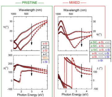
The samples were measured by a Woollam M-2000DI rotating compensator spectroscopic ellipsometer without focusing (the diameter of the spot size was approximately 3 mm), at angles of incidence be- tween 65° and 75°, and photon energies between 1.23 eV and 4.5 eV (Fig. 1) at room temperature in air.
The pristine samples were described by a multilayer model which consists of two pairs of an amorphous Si (a-Si) and C (a-C) layers, a native SiO2layer and a single-crystalline Si (c-Si) substrate (see the inset inFig. 1). There are numerous studies and optical references on a- Si revealing significant differences depending on the way and para- meters of preparation[26,27]. Therefore, instead of using references from databases, the dielectric functions of a-Si and a-C were modeled using the Cody-Lorentz (CL)[28]and the Tauc-Lorentz (TL)[29]os- cillators, respectively. We show below that consistent results can be obtained in spite of the relatively large numbers of fit parameters.
The TL model describes the imaginary part of the dielectric function (ε2) using a convolution of a Lorentz oscillator with a Tauc gap func- tion, which results in the following equation:
Fig. 1.Measured (symbols) and fitted ellipsometry spectra of the original and ion beam-mixed sample. The arrows show the direction of increasing angles of incidence from 65° to 75° in steps of 5°. The insets show the optical models used for calculating the fitted curves.
= + >
E if E E
if E E
( ) ·
0
A E E E
E E E E g
g 2
· · ·( )
( ) ·
1 g
0 2
2 02 2 2 2
(1) where the parametersA,E0,Egand Γ are the amplitude, the peak in the joint density of states, the gap energy and the broadening parameter, respectively, all of them in unit of eV. The real part of the dielectric functionε1is obtained by performing a Kramers-Kronig integration of ε2:
= + P E
E d
( ) 2 ( ) ,
1 1 E 2
2 2
g (2)
wherePstands for the Cauchy principal part of the integral and an additional parameterε1(∞) has been included, set to a constant value of 1 in the calculations.
In the CL model the below-gap region is described by an exponential increase of the absorption with E, the near-gap region is a transition (at energy Et) between features of parabolic bands and a constant dipole matrix element, whereas the above gap region is characterized by Lorentz oscillators, similar to the TL model:
= < <
= + >
E exp if E E
G E L E G E if E E
( ) · 0
( ) ( ) ( )
,
E E
E E
E t
A E
E E E t
2 · · ·E
( ) ·
t µ 1
0
2 02 2 2 2 (3)
whereEtis a transition energy between the Urbach tail and the band-to- band transitions,Eµrepresents the extent of broadening andE1=EtL (Et)G(Et). Here, L(E) is the Lorentz oscillator function andG(E) is a variable band edge function, a result of the constant dipole approach
= +
G E E E
E E E
( ) ( )
( )
g
g p
2
2 2
(4) whereEpis the transition energy that separates the absorption onset behavior from the Lorentzian behavior.
In the ion beam-mixed structure the region close to the surface was divided into sublayers, in which a-SiC, a-Si, and voids were combined using the effective medium approximation (as shown in the right-hand side inset ofFig. 1). In case of the a-SiC the CL model was again used to describe the dispersion of the dielectric function. The CL parameters of a-SiC were fitted together with the volume fractions of the components, whereas the parameters of a-Si were fixed to the values determined from the pristine sample.
Comparing the measured SE spectra on the pristine and mixed layers it can qualitatively be seen that the structure has changed sub- stantially. In the pristine case the oscillations of the spectra are sup- pressed due to the larger extinction and closer index-matching of the adjacent materials.
3. Results
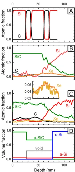
The AES depth profile of the non-irradiated sample is depicted in Fig. 2A. In the pristine sample all interfaces are sharp. The broadening (16–84%) of the interfaces is in the range of 2–3 nm. This means that the intrinsic broadening of the interfaces, which is the combined effect of broadening during sample production and the ion bombardment- induced broadening (during depth profiling) falls in this range. There- fore, any higher value of the interface broadening observed after ion beam modification is due to ion bombardment-induced mixing.
Figs. 2B and C show the depth profiles of the samples irradiated by 120 keV Xe+at a fluence of 3 × 10¹⁶Xe+/cm2calculated using the TRIDYN[22]simulation software and measured by AES, respectively.
The applied irradiation conditions for this layer structure caused a quasi-continuous in-depth distribution of SiC; almost all carbon and silicon atoms formed SiC. We can see that the depth profile obtained by TRIYDN simulation (Fig. 2B) agrees very well with that of the AES measurement (Fig. 2C). This provides an opportunity to design SiC-rich
layers.
The depth profiles inFig. 2D measured by ellipsometry were ob- tained using the optical model shown in the right-hand side inset of Fig. 1. All the thicknesses as well as four CL parameters (amplitude, broadening, gap and oscillator energies) and the volume fractions were fitted simultaneously using a random parameter search in constrained parameter regions followed by a Levenberg-Marquardt gradient fit to find the final values of all the parameters. Since the CL parameters of a- Si were fixed at the pristine values, and the dispersion of a-SiC largely differs from both the a-Si and void components, the parameter un- certainties are typically several percent, despite the fact that fitting dispersion and volume fraction parameters together is usually chal- lenging. Note that a layer of higher disorder below the depth range of interest for the AES-SE comparison also had to be included in the model.
Fig. 2.Concentration depth profiles of pristine (A) and irradiated samples (3 × 10¹⁶Xe+/cm2at a kinetic energy of 120 keV – B, C and D). Figs. B and C show the profiles of SiC, C, Si and Xe calculated by TRIDYN simulation (B) and measured by AES (C). The inset in subfigure C shows the magnified Xe profiles in the depth range from 40 to 90 nm. The deeper orange curve belongs to the calculation. Subfigure (D) shows the depth profiles of a-SiC, a-Si, c-Si and voids determined by fitting the measured SE spectra using the model shown in the inset at the right-hand side ofFig. 1. (For interpretation of the references to colour in this figure legend, the reader is referred to the web version of this article.)
4. Discussion
Thin film characterization methods with depth resolution are based on three different approaches[30]. (1) The first one utilizes removal of surface atoms layer-by-layer (e.g. by sputtering) and measure either the emitted atoms (e.g. secondary ion mass spectrometry) or the remaining surface (AES). (2) The second one is based on a spectroscopic mea- surement which can model the depth profile using sophisticated models based on the large number of measured data from the whole depth of the investigated layer (e.g. Rutherford backscattering spectrometry [RBS], X-ray diffraction or SE). (3) The third approach is to prepare a cross-sectional sample and to measure using a high lateral resolution technique (e.g. electron microscopy, scanning probe methods or Raman spectroscopy).
The methods of groups(1) and (2)can be used in a complementary way, because of the combination of sensitivities on local and long-range properties. For example, it has been shown that RBS and SE are capable of complementary analysis of damage depth profiles[31], in which RBS measured the distribution of the elements but cannot accurately de- termine the thickness and the damage, which can be profiled by SE. The thickness calibration from SE can also be used for accurate determi- nation of the density[32].
In the present case the complementary nature of the applied methods also provides a much richer characterization of the ion mixed layer. As it was shown here and previously[18,19], AES depth profiling is ideal for the determination of the concentration distribution of the elements and compounds. It is also excellent for revealing the com- pound formation during ion mixing. On the other hand, it is not so effective to give an accurate depth scale for the profile. Just in the contrary, SE is not capable of addressing the depth profiling of elements but provides the missing details like the physical density (see the gray curve of voids inFig. 2D) and crystallinity (profiles of a-Si, c-Si and a- SiC). Also, as discussed in the previous section, the layer thicknesses are accurate to nanometers or below. Similarly, the presence of the voids is also a new information concerning the AES depth profiling. In the fol- lowing we will discuss these new SE provided findings.
4.1. Void analysis
Although void profiles can usually be determined by high accuracy using SE in single-crystalline semiconductors (see e.g. Ref.[33]), in this case the uncertainty of the void parameters is relatively large (≈10%) because of the smaller refractive index contrast; still the SE provides an acceptable void profile. The void profile (grey line inFig. 2D) in the depth range from ≈25 to ≈75 nm correlated well with the projected range of the 120-keV Xe+ projectiles (57 ± 14 nm calculated by TRIDYN[22]), as well as with the Xe depth profile revealed by AES in Fig. 2C. Thus, having the AES results as well we can conclude that the SE measures the Xe concentration as voids, and the number of in- evitably present vacancies in the layer is lower than the detection limit of SE. The optical effect of Xe atoms is similar to voids because the chemically inactive non-polarizable inert atoms optically behave like voids. The comparison also shows that the amount of Xe as the volume fraction of voids is overestimated by SE. The effect resembles the one showed for point defects in single-crystalline Si disordered by ion im- plantation of different kinds of noble gases[34,35]. The reason is that the Xe atoms (similar to the point defects) change the dielectric func- tion in a bigger volume than their atomic volume. Therefore, the optical effect of such elements and defects is not proportional to their volume fraction.
4.2. The electronic state of the ion beam-mixed layer
The fitted dielectric functions are plotted in Fig. 3 for both the pristine and the ion beam mixed sample. In the pristine sample the thicknesses and the oscillator parameters of the a-Si and a-C layers are
all fitted in one random search process. The a-Si and a-C dielectric functions as well as the dielectric function resulting from the ion beam mixing (a-SiC) were fitted using the oscillator parameters of Eqs.
(1)–(3). The dielectric function of a-SiC from the mixed sample is very similar to that created by ion implantation amorphization of c-SiC[36]
(see the right-hand side subgraph ofFig. 3). Thenvalues of a-SiC are close to those of c-SiC, butkof a-SiC is ≈1 in the photon energy range between 3 and 4, whereaskof c-SiC is ≈0 in the same range. This is consistent with a large decrease of the optical gap from c-SiC to a-SiC as shown inFig. 3D.
The fitted oscillator parameters are summarized for the pristine and ion beam-mixed samples inTable 1. The similar values for a-Si and a-C are consistent with the similar spectra shown for the pristine sample in Fig. 3A and 3C. The radical optical change during the ion beam process points out potential optical applications of the technique when the ion implantation is combined by masking and structuring of the surface [37]. TheEgvalues of the table can qualitatively be identified from the slopes of thekspectra towards the smaller photon energies in subgraphs 3C and 3D. TheEg= 1.77 for a-SiC is significantly different from that of c-SiC (see thekspectra in graph 3D).
In terms of AES/SE complementarity probably the most character- istic difference is the sensitivity to short-range vs. long-range material properties. AES identifies elements and their chemical states in bonds, Fig. 3.nandk spectra of a-C and a-Si measured on the initial multi-layer sample (left-hand side), as well as that of amorphous SiC created by ion-mixing (right-hand side). The spectra from Ref. [29] created by ion implantation amorphization of single-crystalline SiC (ia-SiC) and of single-crystalline SiC (c- SiC) from Ref.[30]are also plotted for comparison.
Table 1
Fitted oscillator parameters (see Eqs.(1)–(3)for the pristine (a-Si and a-C) and ion beam-mixed (a-SiC) materials. The component a-Si is also used in the ion beam-mixed layers. The spectra calculated from these parameters are plotted in Fig. 3. All parameters are given in units of eV. The uncertainty of theEand Γ parameters are ≈1%, while that ofAfor a-C and a-SiC are ≈30%.Epfor the CL model of a-SiC is fixed at 0.77 eV.
Parameter a-Si a-C a-SiC
Eg 1.58 1.03 1.77
E0 3.23 3.09 6.50
A 86 63 58
Γ 1.93 1.09 9.20
whereas SE is mostly sensitive to their long-range order and properties in larger clusters forming crystals vs. amorphous materials which pri- marily influences how collective electrons form bands [38]. Optical spectra such as those plotted in Fig. 3 are fingerprints of the joint density of electron states in solids that change substantially as the long- range order of atoms are changing in the solids[39]. Similar macro- scopic properties to be detected by SE are the physical density and the layer thickness.
In terms of a reliable comparative and complementary investiga- tion, a useful characteristic of both methods is that the lateral and vertical resolutions are very similar. Both AES and SE integrate areas of millimeters on the surface, but at the same time, both are surface sensitive having nanometer-scale resolution in the vertical direction, being capable of the high accuracy measurement in the top 100 nm of the sample. This fact is of primary importance to make sure that the scales are the same from which the information is collected in different dimensions.
Finally, there are two more important features to be discussed briefly in practical terms of designing new materials. While both methods are highly sensitive for near-surface profiling purposes, there are large differences in speed and non-destructive measurement cap- abilities. While AES destroys the measured layer in a process that takes hours, SE measures it in seconds without any harm or need for special cleaning, preparation and vacuum. It makes SE attractive as a high- speed testing method for the large-scale development of such materials.
Note that if lateral mapping of the properties is an issue, there are only a few methods that provide the combination of that speed and sensi- tivity[40]. Although SE lacks the capability of determining the bond configurations such as AES, by a kind of ‘calibration’ through com- plementary AES/SE measurements it may be capable of the qualifica- tion of even highly complex materials as presented in this article.
5. Conclusion
A sputtered Si/C multilayer structure was transformed into a-SiC by ion beam mixing for optical or protective coating applications. A complementary physicochemical SE/AES profiling approach was ap- plied, in which the AES is responsible for the elementary and chemical analysis, whereas SE shows the accurate layer thicknesses, densities, crystallinity and phases. The combination of the two methods provides a much richer characterization of nanolayers showing inhomogeneity along the depth. The analysis revealed a near-surface region with lower optical density and a structure that has almost completely been trans- formed into SiC. The results point out the possibility of SE to be used as a quick, sensitive and non-destructive testing of similar structures (e.g.
in a manufacturing process).
CRediT authorship contribution statement
P. Petrik: Conceptualization, Data curation, Formal analysis, Funding acquisition, Investigation, Methodology, Visualization, Writing - original draft, Writing - review & editing.A. Racz:Conceptualization, Data curation, Formal analysis, Investigation, Methodology, Writing - original draft.M. Menyhard:Conceptualization, Data curation, Formal analysis, Investigation, Methodology, Writing - original draft.
Declaration of Competing Interest
The authors declare that they have no known competing financial interests or personal relationships that could have appeared to influ- ence the work reported in this paper.
Acknowledgements
Support from National Development Agency grants of OTKA
K131515 is gratefully acknowledged.
References
[1] A. Shypylenko, A.V. Pshyk, B. Grześkowiak, K. Medjanik, B. Peplinska, K. Oyoshi, A. Pogrebnjak, S. Jurga, E. Coy, Effect of ion implantation on the physical and mechanical properties of Ti-Si-N multifunctional coatings for biomedical applica- tions, Mater. Des. 110 (2016) 821–829,https://doi.org/10.1016/j.matdes.2016.08.
[2] N. Ledermann, J. Baborowski, P. Muralt, N. Xantopoulos, J.-M. Tellenbach,050.
Sputtered silicon carbide thin films as protective coating for MEMS applications, Surf. Coat. Technol. 125 (2000) 246–250,https://doi.org/10.1016/S0257- 8972(99)00568-X.
[3] G.F. Eriksen, K. Dyrbye, Protective coatings in harsh environments, J. Micromech.
Microeng. 6 (1996) 55–57,https://doi.org/10.1088/0960-1317/6/1/011.
[4] H. Csorbai, P. Fürjes, G. Hárs, C. Dücső, I. Bársony, E. Kálmán, P. Deák, Microwave- CVD diamond protective coating for 3D structured silicon microsensors, Mater. Sci.
Forum. 414–415 (2003) 69–74,https://doi.org/10.4028/www.scientific.net/MSF.
414-415.69.
[5] V.M.C.A. Oliveira, A.M. Vazquez, C. Aguiar, A. Robin, M.J.R. Barboza, Protective effect of plasma-assisted PVD deposited coatings on Ti–6Al–4V alloy in NaCl solu- tions, Mater. Des. 88 (2015) 1334–1341,https://doi.org/10.1016/j.matdes.2015.
08.158.
[6] W. Daves, A. Krauss, V. Häublein, A.J. Bauer, L. Frey, Enhancement of the stability of Ti and Ni ohmic contacts to 4H-SiC with a stable protective coating for harsh environment applications, J. Electron. Mater. 40 (2011) 1990–1997,https://doi.
org/10.1007/s11664-011-1681-2.
[7] P. Sigmund, A. Gras-Marti, Theoretical aspects of atomic mixing by ion beams, Nucl. Instrum. Methods. 182–183 (1981) 25–41,https://doi.org/10.1016/0029- 554X(81)90668-6.
[8] Á. Barna, S. Gurban, L. Kotis, J. Lábár, A. Sulyok, A.L. Tóth, M. Menyhárd, J. Kovac, P. Panjan, Growth of amorphous SiC film on Si by means of ion beam induced mixing, Appl. Surf. Sci. 263 (2012) 367–372,https://doi.org/10.1016/j.apsusc.
2012.09.063.
[9] T.-K. Nguyen, H.-P. Phan, T. Dinh, K.M. Dowling, A.R.M. Foisal, D.G. Senesky, N.- T. Nguyen, D.V. Dao, Highly sensitive 4H-SiC pressure sensor at cryogenic and elevated temperatures, Mater. Des. 156 (2018) 441–445,https://doi.org/10.1016/
j.matdes.2018.07.014.
[10] H.-P. Phan, H.-H. Cheng, T. Dinh, B. Wood, T.-K. Nguyen, F. Mu, H. Kamble, R. Vadivelu, G. Walker, L. Hold, A. Iacopi, B. Haylock, D.V. Dao, M. Lobino, T. Suga, N.-T. Nguyen, Single-crystalline 3C-SiC anodically bonded onto glass: an excellent platform for high-temperature electronics and bioapplications, ACS Appl. Mater.
Interfaces. 9 (2017) 27365–27371,https://doi.org/10.1021/acsami.7b06661.
[11] R. Cheung, Introduction to silicon carbide (SIC) microelectromechanical systems (MEMS), in: Silicon Carbide Microelectromechanical Syst. Harsh Environ., Published By Imperial College Press and Distributed by World Scientific Publishing Co., 2006: pp. 1–17. https://doi.org/10.1142/9781860949098_0001.
[12] P.M. Sarro, Silicon carbide as a new MEMS technology, Sens. Actuators Phys. 82 (2000) 210–218,https://doi.org/10.1016/S0924-4247(99)00335-0.
[13] I. Laboriante, A. Suwandi, C. Carraro, R. Maboudian, Lubrication of polycrystalline silicon MEMS via a thin silicon carbide coating, Sens. Actuators Phys. 193 (2013) 238–245,https://doi.org/10.1016/j.sna.2013.01.036.
[14] E.A. Filatova, D. Hausmann, S.D. Elliott, Understanding the mechanism of SiC Plasma-Enhanced Chemical Vapor Deposition (PECVD) and Developing Routes to- ward SiC Atomic Layer Deposition (ALD) with Density Functional Theory, ACS Appl. Mater. Interfaces. 10 (2018) 15216–15225,https://doi.org/10.1021/acsami.
8b00794.
[15] W. Daves, A. Krauss, N. Behnel, V. Häublein, A. Bauer, L. Frey, Amorphous silicon carbide thin films (a-SiC:H) deposited by plasma-enhanced chemical vapor de- position as protective coatings for harsh environment applications, Thin Solid Films. 519 (2011) 5892–5898,https://doi.org/10.1016/j.tsf.2011.02.089.
[16] M. Xu, V.M. Ng, S.Y. Huang, J.D. Long, S. Xu, Growth of SiC nanoparticle films by means of RF magnetron sputtering, IEEE Trans. Plasma Sci. 33 (2005) 242–243, https://doi.org/10.1109/TPS.2005.845339.
[17] C.-K. Chung, B.-H. Wu, Thermally induced formation of SiC nanoparticles from Si/
C/Si multilayers deposited by ultra-high-vacuum ion beam sputtering, Nanotechnology. 17 (2006) 3129–3133,https://doi.org/10.1088/0957-4484/17/
13/008.
[18] A.S. Racz, Z. Kerner, A. Nemeth, P. Panjan, L. Peter, A. Sulyok, G. Vertesy, Z. Zolnai, M. Menyhard, Corrosion resistance of nanosized silicon carbide-rich composite coatings produced by noble gas ion mixing, ACS Appl. Mater. Interfaces 9 (2017) 44892–44899,https://doi.org/10.1021/acsami.7b14236.
[19] G. Battistig, S. Gurbán, G. Sáfrán, A. Sulyok, A. Németh, P. Panjan, Z. Zolnai, M. Menyhárd, Wafer-scale SiC rich nano-coating layer by Ar+ and Xe+ ion mixing, Surf. Coat. Technol. 302 (2016) 320–326,https://doi.org/10.1016/j.surfcoat.2016.
06.039.
[20] A.S. Racz, D. Dworschak, M. Valtiner, M. Menyhard, Scratching resistance of SiC- rich nano-coatings produced by noble gas ion mixing, Surf. Coat. Technol. 386 (2020) 125475, ,https://doi.org/10.1016/j.surfcoat.2020.125475.
[21] A.S. Racz, M. Menyhard, Design of corrosion resistive SiC nanolayers, ACS Appl.
Mater. Interfaces. 10 (2018) 22851–22856,https://doi.org/10.1021/acsami.
8b06425.
[22] Möller, Wolfhard, Posselt, Matthias, TRIDYN_FZR User Manual, FZR-317, Forschungszentrum Rossendorf, Dresden, n.d.
[23] W. Möller, W. Eckstein, J.P. Biersack, Tridyn-binary collision simulation of atomic
collisions and dynamic composition changes in solids, Comput. Phys. Commun. 51 (1988) 355–368,https://doi.org/10.1016/0010-4655(88)90148-8.
[24] M. Menyhard, High-depth-resolution Auger depth profiling/atomic mixing, Micron.
30 (1999) 255–265,https://doi.org/10.1016/S0968-4328(99)00010-4.
[25] L. Kotis, M. Menyhard, A. Sulyok, G. Sáfrán, A. Zalar, J. Kovač, P. Panjan, Determination of the relative sputtering yield of carbon to tantalum by means of Auger electron spectroscopy depth profiling, Surf. Interface Anal. 41 (2009) 799–803,https://doi.org/10.1002/sia.3101.
[26] M. Serenyi, T. Lohner, P. Petrik, C. Frigeri, Comparative analysis of amorphous silicon and silicon nitride multilayer by spectroscopic ellipsometry and transmission electron microscopy, Thin Solid Films. 515 (2007) 3559–3562,https://doi.org/10.
1016/j.tsf.2006.10.137.
[27] B. Kalas, Z. Zolnai, G. Safran, M. Serenyi, E. Agocs, T. Lohner, A. Nemeth, M. Fried, P. Petrik, Micro-combinatorial sampling of the optical properties of hydrogenated amorphous Si1−xGex for the entire range of compositions towards a database for optoelectronics, Sci. Rep. under publication (n.d.) 18.
[28] A.S. Ferlauto, G.M. Ferreira, J.M. Pearce, C.R. Wronski, R.W. Collins, X. Deng, G. Ganguly, Analytical model for the optical functions of amorphous semi- conductors from the near-infrared to ultraviolet: Applications in thin film photo- voltaics, J. Appl. Phys. 92 (2002) 2424–2436,https://doi.org/10.1063/1.1497462.
[29] G.E. Jellison, F.A. Modine, Parameterization of the optical functions of amorphous materials in the interband region, Appl. Phys. Lett. 69 (1996) 371–373,https://doi.
org/10.1063/1.118064.
[30] S. Zollner, J.G. Chen, E. Duda, T. Wetteroth, S.R. Wilson, J.N. Hilfiker, Dielectric functions of bulk 4H and 6H {SiC} and spectroscopic ellipsometry studies of thin {SiC} films on Si, J. Appl. Phys. 85 (12) (1999) 8353–8361,https://doi.org/10.
1063/1.370682.
[31] P. Petrik, O. Polgár, M. Fried, T. Lohner, N.Q. Khánh, J. Gyulai, Ellipsometric characterization of damage profiles using an advanced optical model, J. Appl. Phys.
93 (2003) 1987–1990,https://doi.org/10.1063/1.1539306.
[32] E. Szilágyi, P. Petrik, T. Lohner, A.A. Koós, M. Fried, G. Battistig, Oxidation of SiC
investigated by ellipsometry and Rutherford backscattering spectrometry, J. Appl.
Phys. 104 (2008) 014903, ,https://doi.org/10.1063/1.2949268.
[33] P. Petrik, M. Fried, T. Lohner, O. Polgár, J. Gyulai, F. Cayrel, D. Alquier, Optical models for cavity profiles in high-dose helium-implanted and annealed silicon measured by ellipsometry, J. Appl. Phys. 97 (2005) 123514, ,https://doi.org/10.
1063/1.1937469.
[34] P. Petrik, O. Polgar, T. Lohner, M. Fried, N.Q. Khanh, J. Gyulai, E. Ramadan, Ellipsometric characterization of shallow damage profiles created by Xe-implanta- tion into silicon, in: Ion Implant. Technol. 2002 Proc. 14th Int. Conf. On, IEEE, Taos, New Mexico, USA, 2002: pp. 601–604. https://doi.org/10.1109/IIT.2002.1258077.
[35] M. Fried, P. Petrik, T. Lohner, N.Q. Khánh, O. Polgár, J. Gyulai, Dose-dependence of ion implantation-caused damage in silicon measured by ellipsometry and back- scattering spectrometry, Thin Solid Films. 455–456 (2004) 404–409,https://doi.
org/10.1016/j.tsf.2004.01.027.
[36] P. Petrik, E.R. Shaaban, T. Lohner, G. Battistig, M. Fried, J. Garcia Lopez, Y. Morilla, O. Polgár, J. Gyulai, Ion implantation-caused damage in SiC measured by spec- troscopic ellipsometry, Thin Solid Films. 455–456 (2004) 239–243,https://doi.org/
10.1016/j.tsf.2004.01.009.
[37] A.S. Racz, D. Zambo, G. Dobrik, I. Lukacs, Z. Zolnai, A. Nemeth, P. Panjan, A. Deak, G. Battistig, M. Menyhard, Novel method for the production of SiC micro and na- nopatterns, Surf. Coat. Technol. 372 (2019) 427–433,https://doi.org/10.1016/j.
surfcoat.2019.05.061.
[38] P. Petrik, Parameterization of the dielectric function of semiconductor nanocrystals, Phys. B Condens. Matter. 453 (2014) 2–7,https://doi.org/10.1016/j.physb.2014.
03.065.
[39] R.W. Collins, A.S. Ferlauto, 2 Optical Physics of Materials, (n.d.) 204.
[40] A. Shan, M. Fried, G. Juhasz, C. Major, O. Polgar, A. Nemeth, P. Petrik, L.R. Dahal, J. Chen, Z. Huang, N.J. Podraza, R.W. Collins, High-Speed Imaging/Mapping Spectroscopic Ellipsometry for In-Line Analysis of Roll-to-Roll Thin-Film Photovoltaics, IEEE J. Photovolt. 4 (2014) 355–361,https://doi.org/10.1109/
JPHOTOV.2013.2284380.