nanomaterials
Article
Structural Characteristics of the Si Whiskers Grown by Ni-Metal-Induced-Lateral-Crystallization
Béla Pécz1,*, Nikolaos Vouroutzis2, György Zoltán Radnóczi1, Nikolaos Frangis2and John Stoemenos2
Citation: Pécz, B.; Vouroutzis, N.;
Radnóczi, G.Z.; Frangis, N.;
Stoemenos, J. Structural Characteristics of the Si Whiskers Grown by Ni-Metal-Induced-Lateral- Crystallization.Nanomaterials2021, 11, 1878. https://doi.org/10.3390/
nano11081878
Academic Editor: Francesca Iacopi
Received: 30 April 2021 Accepted: 12 July 2021 Published: 22 July 2021
Publisher’s Note:MDPI stays neutral with regard to jurisdictional claims in published maps and institutional affil- iations.
Copyright: © 2021 by the authors.
Licensee MDPI, Basel, Switzerland.
This article is an open access article distributed under the terms and conditions of the Creative Commons Attribution (CC BY) license (https://
creativecommons.org/licenses/by/
4.0/).
1 Centre for Energy Research, Institute for Technical Physics and Materials Science, EK MFA, Konkoly-Thege Miklósút 29-33, 1121 Budapest, Hungary; gy.radn@mfa.kfki.hu
2 Department of Physics, Aristotle University of Thessaloniki, 54124 Thessaloniki, Greece;
nikosv@auth.gr (N.V.); frangis@auth.gr (N.F.); stoimeno@auth.gr (J.S.)
* Correspondence: pecz.bela@ek-cer.hu
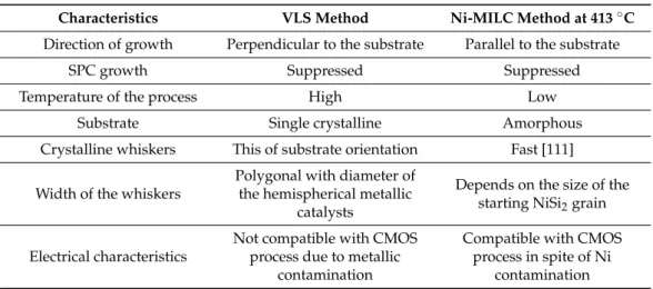
Abstract:Si whiskers grown by Ni-Metal-Induced-Lateral-Crystallization (Ni-MILC) were grown at 413◦C, intentionally below the threshold for Solid State Crystallization, which is 420◦C. These whiskers have significant common characteristics with whiskers grown by the Vapor Liquid Solid (VLS) method. The crystalline quality of the whiskers in both methods is the same. However, in VLS, a crystalline substrate is required, in contrast to the amorphous one in Ni-MILC for the growth of single crystalline whiskers. Moreover, whiskers grown by VLS have a polygonal cross-section with their diameter determined by the diameter of the hemispherical metallic catalysts. On the other hand, in the Ni-MILC, the cross-section of the whiskers depends on the size of the NiSi2grain from which they are emanated. This was confirmed by observing the crossing whiskers and the rotational Moirépatterns in the crossing area. The structure of disturbed short and thin nonlinear branches on the side-walls of the whiskers was studied. In the whiskers grown by the VLS method, significant contamination occurs by the metallic catalyst degrading the electrical characteristics of the whisker.
Such Si whiskers are not compatible with the current CMOS process. Whiskers grown by Ni-MILC at 413◦C are also contaminated by Ni. However, the excess Ni is in the form of tetrahedral NiSi2
inclusions which are coherent with the Si matrix due to the very low misfit of 0.4% between them.
These whiskers are compatible with current CMOS process and Thin Film Transistors (TFTs).
Keywords:crystallization of silicon; transmission electron microscopy; Moiréfringes
1. Introduction
Polycrystalline silicon (poly-Si) films are used in a wide range of applications, such as large-area electronics, including Thin-Film Transistors (TFTs), solar cells and sensors. Solid- Phase-Crystallization (SPC) is one of the simplest methods to crystallize amorphous silicon (a-Si) films, though it requires temperatures above 600◦C [1,2]. In most applications, the substrate is low-cost soft glass which requires lower process temperatures. The crystalliza- tion temperature of a-Si can be lowered by the Ni-Metal-Induced-Lateral-Crystallization (Ni-MILC). For the MILC, the preferred metal up to this date has been nickel (Ni) due to its low residual metal contamination in the poly-Si region [3]. In this case, the a-Si crystallized temperatures can be as low as 413◦C under the presence of nickel-disilicide, NiSi2. The crystallization temperature of a-Si lowers under the presence of NiSi2because Ni atoms from the NiSi2/a-Si interlayer diffuse into a-Si, reducing the strength of the covalent bonds at the interface caused by their interaction with the free electrons from the metallic phase [4].
At the relatively low temperature of 413◦C, whiskers are only grown by Ni-MILC, which makes them worth comparing to those ones grown by the standard VLS method, [5,6].
In the VLS process, the seed for the growth of the Si whisker is a droplet of liquid metal- Si alloy, in most cases this is Au-Si alloy on a (111) Si substrate. The liquid droplet is a preferred site for the Si deposition from the vapor phase; hence, the droplet becomes
Nanomaterials2021,11, 1878. https://doi.org/10.3390/nano11081878 https://www.mdpi.com/journal/nanomaterials
Nanomaterials2021,11, 1878 2 of 14
supersaturated with Si. Subsequently, the excess Si precipitates on the leading face of the Si whisker at the backside of the droplet, resulting in the growth of the Si whisker [5]. In both methods, long single crystalline whiskers are formed. In the VLS case, the isolated whiskers are perpendicular to the substrate, in the MILC case, they are parallel to the substrate and surrounded by a-Si.
In the case of Ni-MILC, the seeds are NiSi2crystallites which are formed after the reaction of Ni with the a-Si film at temperatures as low as 250◦C [7]. The NiSi2is cubic, having the CaF2structure and lattice mismatch with crystalline Si of only 0.4%. During annealing, nickel atoms from the NiSi2seeds diffuse into a-Si, forming new layers of NiSi2 and leaving behind vacancies, accumulated at the backside of the NiSi2grain. Subsequently, a diamond type rearrangement of the Si bonds occurs, resulting in an epitaxial Si layer at the backside of the NiSi2module. This continuous process forms Si whiskers, as described in detail in Refs. [8,9]. In this study, we will show that whiskers grown in a-Si by Ni-MILC at 413 ◦C are similar to those grown by the VLS process. It is worth noticing that the residual Ni contamination of the Si whiskers grown by Ni-MILC is significantly lower in respect to those grown by VLS, where the metal impurity is gold, which is detrimental for electrical properties [10].
We want to note that at high temperature (typically 600◦C), MILC process, also Solid State Crystallization (SPC), happens in a significant way. Namely, the Si whiskers act as seeds facilitating the SPC crystallization around the whiskers (this will be shown later). As this second growth (SPC) process around the whiskers occurs spontaneously, large, highly defected crystallites are formed. The process is described widely in the literature, while the extremely low-temperature case where SPC is completely avoided is worth studying as well.
In order to study the influence of the SPC in the Ni-MILC process, annealing was performed at 600, 555, 490, 454, 420 and 413◦C. In each case, the contribution of the SPC was estimated by Transmission Electron Microscopy (TEM) observation of the mosaic structure development around the whiskers. It was shown that even at 454◦C, the influence of the SPC was noticeable; below 420◦C, no influence of the SPC was observed. These results are included in our previous papers, Refs. [7,11,12]. This should be considered as the threshold of the SPC in Ni-MILC. In the present work, we have studied the structural characteristics of whiskers grown below this threshold, namely at 413◦C, which corresponds to the lowest temperature annealing we have performed. In this manner, we could study the formation of Si nanowires, which is the characteristic of Ni-MILC process, and compare the results to vertical Si nanowires grown on single crystalline silicon by the Au-VLS method.
2. Materials and Methods
The specimen preparation for the Ni-MILC experiment at 413◦C was already pre- sented in detail in Refs. [11,12]. A brief presentation of the procedure is shown schematically in Figure1. The specimens were annealed at 250◦C for 10 min in nitrogen atmosphere for the formation of NiSi2pads, as shown in Figure1f. The nonreacted Ni was etched by HNO3, (Sigma Aldrich, Athens, Greece) Figure1g. The thickness of the deposited Ni film was chosen to give stoichiometric NiSi2to all the depth of the a-Si film. In this way, a pattern of NiSi2pads was formed. Annealing was performed for the realization of the Ni-MILC process. For this purpose, samples with dimensions of 15 mm×6 mm were placed in quartz ampoules which were sealed in vacuum {8×10⁻²(Pa)} and annealed at 413◦C for 11 Ds (days), and for 32 Ds. Annealing was performed in an oven equipped with a temperature controller; moreover, a thermocouple was also used to check the actual temperature of the specimens. The accuracy of the temperature measurement is±1◦C.
Conventional MILC specimens were annealed at 520◦C for 1 h in nitrogen atmosphere for reference purposes. Specimens for Plane View TEM (PVTEM) observations were prepared by etching the capping protection SiO2layer, the SiO2buffer layer and the glass substrate using HF (Sigma Aldrich, Athens, Greece) and subsequently lifting off the Si film on gold micro-grids. For the structural characterization, a 2010 JEM microscope (JEOL Corp. Tokyo,
Nanomaterials2021,11, 1878 3 of 14
Japan) as well as a Thermo Fisher THEMIS 200 image corrected microscope (Eindhoven, The Netherlands) was used.
Nanomaterials 2021, 11, x FOR PEER REVIEW 3 of 14
using HF (Sigma Aldrich, Athens, Greece) and subsequently lifting off the Si film on gold micro-grids. For the structural characterization, a 2010 JEM microscope (JEOL Corp. To- kyo, Japan) as well as a Thermo Fisher THEMIS 200 image corrected microscope (Eindho- ven, The Netherlands) was used.
Figure 1. Schematic representation of the specimen preparation for the Ni-MILC experiment at 413
°C. (a) Deposition of 200 nm thick SiO2 buffer layer on glass substrate by PECVD. (b) Deposition of 50 nm a-Si by LPCVD. (c) Deposition of a 50 nm thick SiO2 capping layer by PECVD. (d) Open windows in the SiO2 capping layer for the pad formation. (e) Deposition of 15 nm thick nickel. (f) Annealing at 250 °C for 10 min in order to form polycrystalline NiSi2 in the area of the windows. (g) The nonreacted Ni is etched by HNO3.
3. Results and Discussion
A Si whisker grown by Ni-MILC at 413 °C is not affected by Solid Phase Crystalliza- tion (SPC) [7,11]. In contrast, the same process in the range of temperatures 500–600 °C is strongly affected by SPC, creating a high density of defects. Therefore, the absence of SPC at Ni-MILC at 413 °C results in better quality Si whiskers comparable to those grown by the VLS method.
At first glance, the contribution of SPC in Ni-MILC should be insignificant because the incubation period for random nucleation at 600 °C is more than 10 h [2]. However, the incubation period for a-Si crystallization in Ni-MILC is zero, as was shown by an in situ TEM experiment, Radnoczi et al. [7]. Therefore, SPC is significant in Ni-MILC because the pre-existing whiskers act as seeds for crystallization unless the annealing temperature is sufficiently low to prevent the crystallization.
The contribution of the SPC at 520 °C is shown in the TEM micrographs in Figure 2a,b. Figure 2a shows the formation of Si whiskers in the areas denoted by the letters D and F after annealing for 2 min. The same areas are shown in Figure 2b 6 min later. Now, the whiskers are surrounded by misoriented Si grains due to SPC using the whiskers as seeds. The significance of SPC in Ni-MILC above 500 °C is shown in the high magnifica- tion micrograph in Figure 2c where the whiskers are surrounded by slightly misoriented Figure 1. Schematic representation of the specimen preparation for the Ni-MILC experiment at 413◦C. (a) Deposition of 200 nm thick SiO2buffer layer on glass substrate by PECVD. (b) Deposition of 50 nm a-Si by LPCVD. (c) Deposition of a 50 nm thick SiO2capping layer by PECVD. (d) Open windows in the SiO2 capping layer for the pad formation. (e) Deposition of 15 nm thick nickel.
(f) Annealing at 250◦C for 10 min in order to form polycrystalline NiSi2in the area of the windows.
(g) The nonreacted Ni is etched by HNO3.
3. Results and Discussion
A Si whisker grown by Ni-MILC at 413◦C is not affected by Solid Phase Crystallization (SPC) [7,11]. In contrast, the same process in the range of temperatures 500–600◦C is strongly affected by SPC, creating a high density of defects. Therefore, the absence of SPC at Ni-MILC at 413◦C results in better quality Si whiskers comparable to those grown by the VLS method.
At first glance, the contribution of SPC in Ni-MILC should be insignificant because the incubation period for random nucleation at 600◦C is more than 10 h [2]. However, the incubation period for a-Si crystallization in Ni-MILC is zero, as was shown by an in situ TEM experiment, Radnoczi et al. [7]. Therefore, SPC is significant in Ni-MILC because the pre-existing whiskers act as seeds for crystallization unless the annealing temperature is sufficiently low to prevent the crystallization.
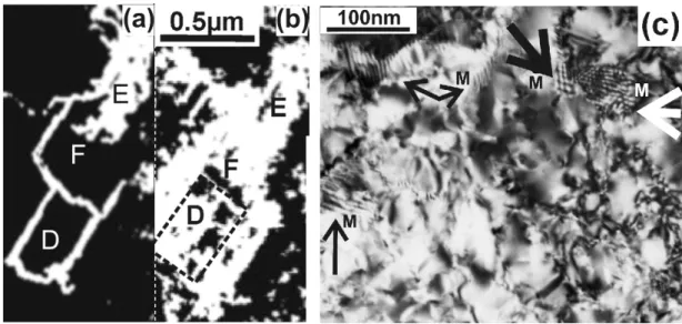
The contribution of the SPC at 520◦C is shown in the TEM micrographs in Figure2a,b.
Figure2a shows the formation of Si whiskers in the areas denoted by the letters D and F after annealing for 2 min. The same areas are shown in Figure2b 6 min later. Now, the whiskers are surrounded by misoriented Si grains due to SPC using the whiskers as seeds. The significance of SPC in Ni-MILC above 500◦C is shown in the high magnification micrograph in Figure2c where the whiskers are surrounded by slightly misoriented grains, resulting in a mosaic structure. Overlapping grains give a Moirépattern of rotational type [13], which
Nanomaterials2021,11, 1878 4 of 14
is denoted by the letter M in Figure2c. More details on the SPC involvement in Ni-MILC above 500◦C are shown by M. Miyasaka et al. [14], also by Radnoczi, G.Z. et al. [7].
Nanomaterials 2021, 11, x FOR PEER REVIEW 4 of 14
grains, resulting in a mosaic structure. Overlapping grains give a Moiré pattern of rota- tional type [13], which is denoted by the letter M in Figure 2c. More details on the SPC involvement in Ni-MILC above 500 °C are shown by M. Miyasaka et al. [14], also by Rad- noczi, G.Z. et al. [7].
Figure 2. TEM micrographs from in situ Ni-MILC at 520 °C where SPC is significant. (a) In the areas D and F, Si whiskers are evident, frequently changing direction, forming a loop in area D. (b) The same area 2 min later, the areas D and F are covered by slightly misoriented grains due to SPC. (c) Slightly misoriented overlapping grains due to the SPC process give Moiré patterns of rotational type shown by arrows.
3.1. Tweed-Like Structure in Ni-MILC at 413 °C
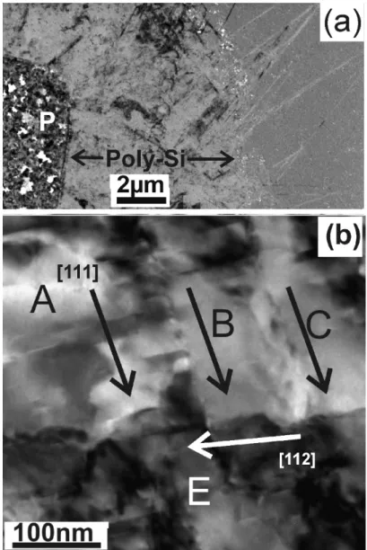
The SPC process can be completely inhibited by lowering the annealing temperature to 413 °C, resulting in pure Ni-MILC. The films consist of a mixture of whiskers growing fast along the [111] crystallographic direction and whiskers grown slowly, having random crystallographic orientations, other than the [111] [5]. The overall view of such a film is shown at the low magnification micrographs in Figure 3a. The NiSi2 pad, denoted by the letter P, is surrounded by a net of fast [111] type and slow type whiskers, resulting in a tweed-like structure; this is shown in the high magnification macrograph in Figure 3b, where three parallel fast [111] whiskers, A, B, C, are intersected by the slow [112] whisker E. At the edges of the tweed-like film, bands of long parallel [111] type whiskers are ob- served as shown in Figure 3a. This is the result of the natural crystal filtering due to growth-velocity competition which is observed when grains meet other grains that have already been crystallized [13,14]. The observed long whiskers must be exactly parallel to the substrate; otherwise, they touch the surface or the bottom of the film and stop. Whisk- ers as long as 9 μm were observed, as shown in Figure 3a. The crystal filtering effect was also observed in the Ni-MILC at 550 °C, where SPC is also involved, by artificial preferred filtration through a narrow neck in the a-Si which was formed artificially by lithography, creating a SiO2 barrier in the a-Si, before the onset of Ni-MILC [14].
Figure 2.TEM micrographs from in situ Ni-MILC at 520◦C where SPC is significant. (a) In the areas D and F, Si whiskers are evident, frequently changing direction, forming a loop in area D. (b) The same area 2 min later, the areas D and F are covered by slightly misoriented grains due to SPC. (c) Slightly misoriented overlapping grains due to the SPC process give Moirépatterns of rotational type shown by arrows.
3.1. Tweed-Like Structure in Ni-MILC at 413◦C
The SPC process can be completely inhibited by lowering the annealing temperature to 413◦C, resulting in pure Ni-MILC. The films consist of a mixture of whiskers growing fast along the [111] crystallographic direction and whiskers grown slowly, having random crystallographic orientations, other than the [111] [5]. The overall view of such a film is shown at the low magnification micrographs in Figure3a. The NiSi2pad, denoted by the letter P, is surrounded by a net of fast [111] type and slow type whiskers, resulting in a tweed-like structure; this is shown in the high magnification macrograph in Figure3b, where three parallel fast [111] whiskers, A, B, C, are intersected by the slow [112] whisker E. At the edges of the tweed-like film, bands of long parallel [111] type whiskers are observed as shown in Figure3a. This is the result of the natural crystal filtering due to growth-velocity competition which is observed when grains meet other grains that have already been crystallized [13,14]. The observed long whiskers must be exactly parallel to the substrate; otherwise, they touch the surface or the bottom of the film and stop. Whiskers as long as 9µm were observed, as shown in Figure3a. The crystal filtering effect was also observed in the Ni-MILC at 550◦C, where SPC is also involved, by artificial preferred filtration through a narrow neck in the a-Si which was formed artificially by lithography, creating a SiO2barrier in the a-Si, before the onset of Ni-MILC [15,16].
Nanomaterials2021,11, 1878 5 of 14
Nanomaterials 2021, 11, x FOR PEER REVIEW 5 of 14
Figure 3. TEM micrographs from Ni-MILC at 413 °C where SPC is completely suppressed. (a) Over- all view of the structure around the pad denoted by the letter P. A continuous poly-Si film consisting of a mixture of fast and slow whiskers resulting in a tweed-like structure is extended up to 8 μ.
Then, long fast [111] type whiskers emanate due to growth–death competition mechanism. (b) The tweed-like structure shown at higher magnification.
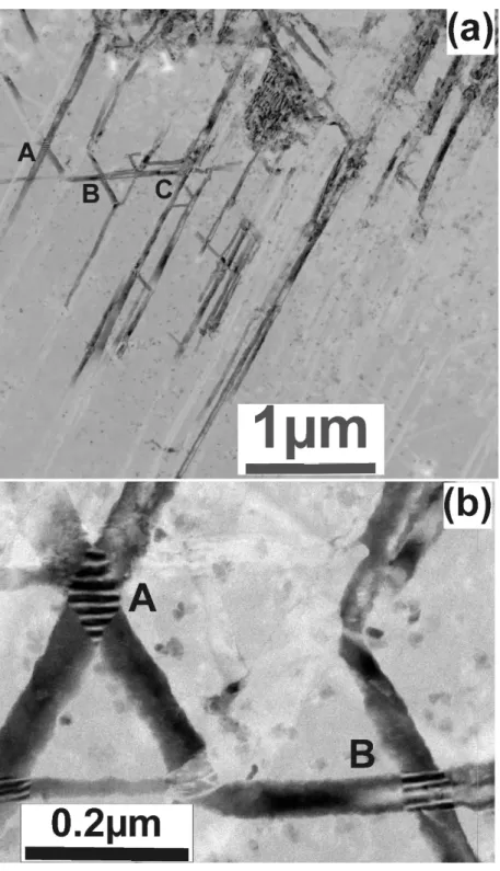
3.2. Crossover of the Whiskers in Ni-MILC at 413 °C
In some cases, the whiskers can cross each other, as shown in Figure 4a, denoted by the letters A, B and C. Very often, Moiré patterns are formed in the crossing area, revealing overlapping of the whiskers in this area. This is evident in the areas A and B, as shown in the higher magnification micrograph of Figure 4b.
Figure 3.TEM micrographs from Ni-MILC at 413◦C where SPC is completely suppressed. (a) Overall view of the structure around the pad denoted by the letter P. A continuous poly-Si film consisting of a mixture of fast and slow whiskers resulting in a tweed-like structure is extended up to 8µ. Then, long fast [111] type whiskers emanate due to growth–death competition mechanism. (b) The tweed-like structure shown at higher magnification.
3.2. Crossover of the Whiskers in Ni-MILC at 413◦C
In some cases, the whiskers can cross each other, as shown in Figure4a, denoted by the letters A, B and C. Very often, Moirépatterns are formed in the crossing area, revealing overlapping of the whiskers in this area. This is evident in the areas A and B, as shown in the higher magnification micrograph of Figure4b.
The formation of Moirépatterns in two crossing whiskers was systematically studied as shown in Figure5a; the crossing whiskers are denoted by the letters A and B. The diffrac- tion pattern in the inset of Figure5a was taken from the crossing area and corresponds to the (112) zone, revealing that the whisker A grows along the [111] direction; in other words, it is a fast type whisker. The reflection 220 is common for both whiskers and is split, making a small angle of about 3.5◦. These double spots create the Moirépatterns in the crossing area. The Moirépatterns are extended perpendicular to theg220reflection, namely along the [111] direction. Therefore, the Moirépatterns are of the rotation type [13], having a periodicity of 2.7 nm. The direction of growth of the whisker B is the [112]. This was deduced considering the angle which it forms with whisker A and with the common
Nanomaterials2021,11, 1878 6 of 14
direction [110]. These are 62◦and 30◦, respectively; only the [112] direction forms such angles with the [111] and [110] directions. Therefore, the whisker B is a slow type whisker.
Nanomaterials 2021, 11, x FOR PEER REVIEW 6 of 14
Figure 4. TEM micrographs. (a) Overall view of crossing whiskers; in some cases, the same whisker crosses several whiskers having different orientations denoted by the letters A, B and C. (b) The crossing areas A and B at higher magnification reveal the formation of Moiré fringes.
The formation of Moiré patterns in two crossing whiskers was systematically studied as shown in Figure 5a; the crossing whiskers are denoted by the letters A and B. The dif- fraction pattern in the inset of Figure 5a was taken from the crossing area and corresponds to the (112) zone, revealing that the whisker A grows along the [111] direction; in other words, it is a fast type whisker. The reflection 220 is common for both whiskers and is split, making a small angle of about 3.5°. These double spots create the Moiré patterns in the crossing area. The Moiré patterns are extended perpendicular to the g220 reflection, namelyalong the [111] direction. Therefore, the Moiré patterns are of the rotation type [13], having a periodicity of 2.7 nm. The direction of growth of the whisker B is the [112].
Figure 4.TEM micrographs. (a) Overall view of crossing whiskers; in some cases, the same whisker crosses several whiskers having different orientations denoted by the letters A, B and C. (b) The crossing areas A and B at higher magnification reveal the formation of Moiréfringes.
Nanomaterials2021,11, 1878 7 of 14
Nanomaterials 2021, 11, x FOR PEER REVIEW 7 of 14
This was deduced considering the angle which it forms with whisker A and with the com- mon direction [110]. These are 62° and 30°, respectively; only the [112] direction forms such angles with the [111] and [110] directions. Therefore, the whisker B is a slow type whisker.
Figure 5. (a) High magnification TEM micrograph from the crossing area of two whiskers A and B in the inset is the corresponding diffraction pattern. The two whiskers have common reflection of 220, which is split; the Moiré fringes are perpendicular to this reflection, revealing that they are of the rotational type. (b) Schematic representation in 3D of two overlapping whiskers emanating from the NiSi2 pad. The total thickness of the overlapping whiskers A and B must not exceed the thickness of the film.
A more accurate estimation of the misorientation of the two whiskers can be deduced by applying the equation
θ = d/D (1)
where D is the periodicity of the Moiré patterns, d the spacing of the lattice planes of the operating diffraction, in our case d220 = 0.192 nm and θ the angle of the misorientation in rad. For D = 2.7 nm, we have θ = 0.071 rad = 4.07°; this is the exact angle between the split 220 spots. The overlap of the two whiskers A and B is shown schematically in 3D in Figure 5b. The total thickness of the overlapping whiskers A and B must not exceed the thickness of the film, which is 50 nm.
According to Equation (1), when the overlapping whiskers form a relatively large misorientation angle θ, the periodicity of the rotational Moiré patterns is small, requiring high-resolution TEM to be revealed; this is shown in the high-resolution TEM micrograph in Figure 6. In this case, two fast [111] type whiskers A and B partially overlap, creating rotational Moiré patterns with periodicity D111 = 1.38 nm, as shown in Figure 6. The miso- rientation angle θ was calculated from Equation (1) with common reflection 111, (d111 = 0.3138 nm), resulting in θ = 13.035°. Since the whiskers A and B have the (110) zone axis, Figure 5.(a) High magnification TEM micrograph from the crossing area of two whiskers A and B in the inset is the corresponding diffraction pattern. The two whiskers have common reflection of 220, which is split; the Moiréfringes are perpendicular to this reflection, revealing that they are of the rotational type. (b) Schematic representation in 3D of two overlapping whiskers emanating from the NiSi2pad. The total thickness of the overlapping whiskers A and B must not exceed the thickness of the film.
A more accurate estimation of the misorientation of the two whiskers can be deduced by applying the equation
θ= d/D (1)
where D is the periodicity of the Moirépatterns, d the spacing of the lattice planes of the operating diffraction, in our case d220= 0.192 nm andθthe angle of the misorientation in rad. For D = 2.7 nm, we haveθ= 0.071 rad = 4.07◦; this is the exact angle between the split 220 spots. The overlap of the two whiskers A and B is shown schematically in 3D in Figure5b. The total thickness of the overlapping whiskers A and B must not exceed the thickness of the film, which is 50 nm.
According to Equation (1), when the overlapping whiskers form a relatively large misorientation angleθ, the periodicity of the rotational Moirépatterns is small, requiring high-resolution TEM to be revealed; this is shown in the high-resolution TEM micrograph in Figure6. In this case, two fast [111] type whiskers A and B partially overlap, creating rotational Moirépatterns with periodicity D111 = 1.38 nm, as shown in Figure6. The misorientation angleθ was calculated from Equation (1) with common reflection 111, (d111= 0.3138 nm), resulting inθ= 13.035◦. Since the whiskers A and B have the (110) zone axis, they also have the reflections 220 and 002 in common; therefore, rotation type Moiré should also be observed from these reflections. It is worth noticing that the 200 reflection is forbidden in the diamond structure; however, it appears, especially in the section (110) due to double reflection of the 111 and 111 spots; that is why it is denoted with a star (*).
However, the Moirépatterns are intense only for reflections which are close to the “two
Nanomaterials2021,11, 1878 8 of 14
beam” case, fading fast outside of it. This is the case in Figure6, where only one set of Moirépatterns is observed.
Nanomaterials 2021, 11, x FOR PEER REVIEW 8 of 14
they also have the reflections 220 and 002 in common; therefore, rotation type Moiré should also be observed from these reflections. It is worth noticing that the 200 reflection is forbidden in the diamond structure; however, it appears, especially in the section (110) due to double reflection of the 111 and 111 spots; that is why it is denoted with a star (*).
However, the Moiré patterns are intense only for reflections which are close to the “two beam” case, fading fast outside of it. This is the case in Figure 6, where only one set of Moiré patterns is observed.
Figure 6. High-resolution TEM micrograph from two partially overlapping [111] type whiskers A and B; the overlapping area is denoted by the letter C. The observed rotational Moiré pattern has a periodicity of D111 = 1.38 nm.
Another example of two partially overlapping parallel whiskers, A and B, is shown in Figure 7. The related diffraction pattern in the inset of Figure 7 confirms that the parallel whiskers A and B are of the slow type, grown along the [110] direction with their (110) planes perpendicular to the electron beam. The periodicity of the Moiré pattern is 11 nm, also running parallel to this direction, revealing that they are created from the strong 002 reflection which is perpendicular to the [110] direction. According to Equation (1), the angle of rotation θ for the reflection 002 is only 1.4°, too small to be distinguished in the diffraction pattern.
Figure 7. TEM micrograph of two partially overlapping parallel whiskers A and B. The related dif- fraction pattern in the inset reveals that the parallel whiskers A and B are in the (110) section, grown along the [110] direction, and therefore are of the slow type.
The cross-section of the whiskers grown by VLS are symmetric polygonal, growing from a single crystalline Si substrate [5]. In contrast, in the Ni-MILC, the Si whiskers grow from NiSi2 grains which have different size, shape and orientation. This explains why two whiskers having width of about 50 nm, as shown in Figure 5a, can overlap in a 50 nm Figure 6.High-resolution TEM micrograph from two partially overlapping [111] type whiskers A and B; the overlapping area is denoted by the letter C. The observed rotational Moirépattern has a periodicity of D111= 1.38 nm.
Another example of two partially overlapping parallel whiskers, A and B, is shown in Figure7. The related diffraction pattern in the inset of Figure7confirms that the parallel whiskers A and B are of the slow type, grown along the [110] direction with their (110) planes perpendicular to the electron beam. The periodicity of the Moirépattern is 11 nm, also running parallel to this direction, revealing that they are created from the strong 002 reflection which is perpendicular to the [110] direction. According to Equation (1), the angle of rotationθfor the reflection 002 is only 1.4◦, too small to be distinguished in the diffraction pattern.
Nanomaterials 2021, 11, x FOR PEER REVIEW 8 of 14
they also have the reflections 220 and 002 in common; therefore, rotation type Moiré should also be observed from these reflections. It is worth noticing that the 200 reflection is forbidden in the diamond structure; however, it appears, especially in the section (110) due to double reflection of the 111 and 111 spots; that is why it is denoted with a star (*).
However, the Moiré patterns are intense only for reflections which are close to the “two beam” case, fading fast outside of it. This is the case in Figure 6, where only one set of Moiré patterns is observed.
Figure 6. High-resolution TEM micrograph from two partially overlapping [111] type whiskers A and B; the overlapping area is denoted by the letter C. The observed rotational Moiré pattern has a periodicity of D111 = 1.38 nm.
Another example of two partially overlapping parallel whiskers, A and B, is shown in Figure 7. The related diffraction pattern in the inset of Figure 7 confirms that the parallel whiskers A and B are of the slow type, grown along the [110] direction with their (110) planes perpendicular to the electron beam. The periodicity of the Moiré pattern is 11 nm, also running parallel to this direction, revealing that they are created from the strong 002 reflection which is perpendicular to the [110] direction. According to Equation (1), the angle of rotation θ for the reflection 002 is only 1.4°, too small to be distinguished in the diffraction pattern.
Figure 7. TEM micrograph of two partially overlapping parallel whiskers A and B. The related dif- fraction pattern in the inset reveals that the parallel whiskers A and B are in the (110) section, grown along the [110] direction, and therefore are of the slow type.
The cross-section of the whiskers grown by VLS are symmetric polygonal, growing from a single crystalline Si substrate [5]. In contrast, in the Ni-MILC, the Si whiskers grow from NiSi2 grains which have different size, shape and orientation. This explains why two whiskers having width of about 50 nm, as shown in Figure 5a, can overlap in a 50 nm Figure 7. TEM micrograph of two partially overlapping parallel whiskers A and B. The related diffraction pattern in the inset reveals that the parallel whiskers A and B are in the (110) section, grown along the [110] direction, and therefore are of the slow type.
The cross-section of the whiskers grown by VLS are symmetric polygonal, growing from a single crystalline Si substrate [5]. In contrast, in the Ni-MILC, the Si whiskers grow from NiSi2grains which have different size, shape and orientation. This explains why two whiskers having width of about 50 nm, as shown in Figure5a, can overlap in a 50 nm thick film. Obviously, the cross-section of the whiskers in Ni-MILC is not symmetric polygonal, as shown schematically in the 3D Figure5b. This is a significant dissimilarity in the two processes.
The Moirépatterns are very sensitive to any lattice misorientation. The exclusion of the SPC process results in homogeneous Moirépatterns in the overlapping whiskers.
Nanomaterials2021,11, 1878 9 of 14
If the overlapping whiskers are also affected by the SPC process causing random small misorientations (Ni-MILC temperature above 500◦C), then the overlapping area would be divided into smaller areas, exhibiting rotational Moirépatterns of different periodicity and orientation due to the misoriented grains as shown in Figure2c.
3.3. Width of the Whiskers
Whiskers grown by VLS have polygonal cross-section with a diameter determined by the diameter D of the hemispherical metallic catalysts according to the equation:
D = 4VLσLV/RT ln(s) (2)
where VLis the molar volume of the metallic droplet,σLVthe liquid-vapor surface energy and s the degree of supersaturation of the vapor [10]. Nevertheless, Oswald ripening mechanism leads to the formation of larger droplets of metal catalyst. On the other hand, in the Ni-MILC case the cross-section of the whiskers depends on the size of the NiSi2grain from which they are emanated. Thus, the mean size of the grains in the NiSi2pads grown at 250◦C is 60 nm, but most of them are below 50 nm in the perpendicular direction as schematically shown in Figure5b. The cross-section of the Si whiskers is fitted to the facet of NiSi2grain from which they are emanated. Therefore, the whiskers are not symmetrical, as already schematically described in Figure5b.
3.4. Saw-Tooth Faceting of the Side-Walls of the Whiskers
In the fast <111> whiskers grown by Ni-MILC, saw-tooth faceting of the side-walls is frequently observed, with the longest segments of the tooth to be the (111) planes, as shown in Figure8. Similar structures were observed in whiskers grown by VLS [5]. Saw-tooth faceting occurs when the side-walls are not stable; namely, they do not belong to the equilibrium crystal shape. In this case, the surface breaks into stable saw-tooth facets [17].
Nanomaterials 2021, 11, x FOR PEER REVIEW 9 of 14
thick film. Obviously, the cross-section of the whiskers in Ni-MILC is not symmetric po- lygonal, as shown schematically in the 3D Figure 5b. This is a significant dissimilarity in the two processes.
The Moiré patterns are very sensitive to any lattice misorientation. The exclusion of the SPC process results in homogeneous Moiré patterns in the overlapping whiskers. If the overlapping whiskers are also affected by the SPC process causing random small mis- orientations (Ni-MILC temperature above 500 °C), then the overlapping area would be divided into smaller areas, exhibiting rotational Moiré patterns of different periodicity and orientation due to the misoriented grains as shown in Figure 2c.
3.3. Width of the Whiskers
Whiskers grown by VLS have polygonal cross-section with a diameter determined by the diameter D of the hemispherical metallic catalysts according to the equation:
D = 4VLσLV/RT ln(s) (2)
where VL is the molar volume of the metallic droplet, σLV the liquid-vapor surface energy and s the degree of supersaturation of the vapor [10]. Nevertheless, Oswald ripening mechanism leads to the formation of larger droplets of metal catalyst. On the other hand, in the Ni-MILC case the cross-section of the whiskers depends on the size of the NiSi2 grain from which they are emanated. Thus, the mean size of the grains in the NiSi2 pads grown at 250 °C is 60 nm, but most of them are below 50 nm in the perpendicular direction as schematically shown in Figure 5b. The cross-section of the Si whiskers is fitted to the facet of NiSi2 grain from which they are emanated. Therefore, the whiskers are not sym- metrical, as already schematically described in Figure 5b.
3.4. Saw-Tooth Faceting of the Side-Walls of the Whiskers
In the fast <111> whiskers grown by Ni-MILC, saw-tooth faceting of the side-walls is frequently observed, with the longest segments of the tooth to be the (111) planes, as shown in Figure 8. Similar structures were observed in whiskers grown by VLS [5]. Saw- tooth faceting occurs when the side-walls are not stable; namely, they do not belong to the equilibrium crystal shape. In this case, the surface breaks into stable saw-tooth facets [17].
Figure 8. Cross-section TEM micrograph from fast [111] whiskers viewed in (110) section. A saw-tooth faceting of the side- walls is evident, with the longest segments of the tooth being the (111) planes.
3.5. Straight Whiskers in Ni-MILC at 413 °C
In Ni-MILC above 520 °C, the fast [111] type whiskers prevail, changing their course frequently to other equivalent <111> directions, facilitating in this way the crystallization [13], as shown in the TEM micrograph in Figure 2a,b. In contrast, the whiskers in Ni-MILC at 413 °C are, in general, straight, rarely changing their course as shown in Figures 3a and 4a. It is speculated that the reason for this difference is the extra dangling bonds which are required when a [111] whisker changes its course to another equivalent direction, say Figure 8. Cross-section TEM micrograph from fast [111] whiskers viewed in (110) section. A saw-tooth faceting of the side-walls is evident, with the longest segments of the tooth being the (111) planes.
3.5. Straight Whiskers in Ni-MILC at 413◦C
In Ni-MILC above 520◦C, the fast [111] type whiskers prevail, changing their course frequently to other equivalent <111> directions, facilitating in this way the crystalliza- tion [13], as shown in the TEM micrograph in Figure2a,b. In contrast, the whiskers in Ni-MILC at 413◦C are, in general, straight, rarely changing their course as shown in Figures3a and4a. It is speculated that the reason for this difference is the extra dangling bonds which are required when a [111] whisker changes its course to another equivalent direction, say the [111] as schematically shown in Figure9. The whisker A is a fast [111]
one growing linearly to a length L; the whisker B is also fast, having the same length, which during the growth was switched to another equivalent [111] direction. For the switching, an extra part is required, denoted by red in Figure9. Therefore, extra dangling bonds are created for the same length, making this change unfavorable from the energetic point of
Nanomaterials2021,11, 1878 10 of 14
view, especially at lower temperatures. The switching to the [111] direction is also shown in the schematic atomic representation viewed in the (110) section in Figure9. The extra dangling bonds included in the red area are evident. It is worth noticing that the Ni-MILC at 413◦C is a very slow process permitting the atoms to find the lowest energy position minimizing the dangling bonds and resulting in straight whiskers as in VLS. This is not the case in the conventional Ni-MILC above 520◦C where significant SPC occurs. In this case, the <111> whiskers change their course frequently to another equivalent <111> direction, facilitating, in this way, the crystallization of the intermediate amorphous space by SPC growth as it is shown in Figure2; see also M. Miyasaka et al. [14]. This is a consequence of the minimum action principle, namely the system takes the lower energy state in the minimum time.
Nanomaterials 2021, 11, x FOR PEER REVIEW 10 of 14
the [111] as schematically shown in Figure 9. The whisker A is a fast [111] one growing linearly to a length L; the whisker B is also fast, having the same length, which during the growth was switched to another equivalent [111] direction. For the switching, an extra part is required, denoted by red in Figure 9. Therefore, extra dangling bonds are created for the same length, making this change unfavorable from the energetic point of view, especially at lower temperatures. The switching to the [111] direction is also shown in the schematic atomic representation viewed in the (110) section in Figure 9. The extra dan- gling bonds included in the red area are evident. It is worth noticing that the Ni-MILC at 413 °C is a very slow process permitting the atoms to find the lowest energy position min- imizing the dangling bonds and resulting in straight whiskers as in VLS. This is not the case in the conventional Ni-MILC above 520 °C where significant SPC occurs. In this case, the <111> whiskers change their course frequently to another equivalent <111> direction, facilitating, in this way, the crystallization of the intermediate amorphous space by SPC growth as it is shown in Figure 2; see also M. Miyasaka et al. [14]. This is a consequence of the minimum action principle, namely the system takes the lower energy state in the minimum time.
Figure 9. Schematic representation of a fast [111] whisker denoted by the letter A which grows lin- early having a length L. Compare this whisker with the whisker B having the same total length L.
During the growth, the whisker B switches to the equivalent [111] direction. Although the two whiskers have the same length, an extra part denoted by red is required for the switching, including the formation of extra dangling bonds. This is also shown schematically in atomic scale in the section (110).
3.6. Disturbed Ni-MILC at 413 °C
Figure 9. Schematic representation of a fast [111] whisker denoted by the letter A which grows linearly having a length L. Compare this whisker with the whisker B having the same total length L. During the growth, the whisker B switches to the equivalent [111] direction. Although the two whiskers have the same length, an extra part denoted by red is required for the switching, including the formation of extra dangling bonds. This is also shown schematically in atomic scale in the section (110).
3.6. Disturbed Ni-MILC at 413◦C
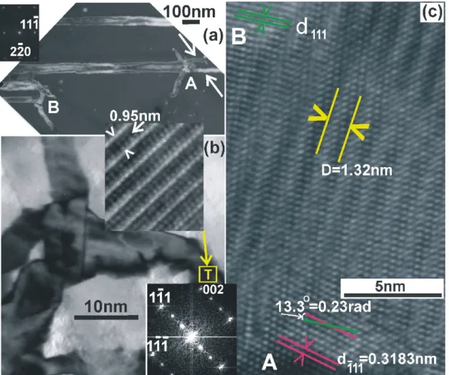
In some cases, the Ni-MILC at 413◦C is disturbed so that short and thin nonlinear branches appear at the side-walls of the whisker as shown in the whiskers A and B in the DF-PVTEM micrograph in Figure10a. It is speculated that the disturbance of the crystallization is due to contamination. Similarly, side-wall branches were observed due to contamination in nanowires grown by VLS [5]. In Figure10a, in the area A, the formation of these branches is followed by splitting of the original whisker into two thinner ones, which
Nanomaterials2021,11, 1878 11 of 14
are parallel to the original. In the region B, the crystallization stops after the formation of the side-wall branches. These branches are microcrystalline, consisting of grains having a mean size of 7 nm as shown in Figure10b. In the grain denoted by the letter T in Figure10b, a pattern with periodicity of three times the d111spacing of the Si lattice, D = 3d111= 0.95 nm, was observed along the direction [111]. This is confirmed by the extra spots in the Fast Fourier Transform (FFT) shown in the inset, in the bottom of Figure10b. This is not a superlattice structure in Si; they are simply Moirépatterns which are formed by double diffraction of the electron beam in the Si matrix and an overlapping (111) type twin, i.e., a Σ3 type twin, viewed in the (110) section.
Nanomaterials 2021, 11, x FOR PEER REVIEW 11 of 14
In some cases, the Ni-MILC at 413 °C is disturbed so that short and thin nonlinear branches appear at the side-walls of the whisker as shown in the whiskers A and B in the DF-PVTEM micrograph in Figure 10a. It is speculated that the disturbance of the crystal- lization is due to contamination. Similarly, side-wall branches were observed due to con- tamination in nanowires grown by VLS [5]. In Figure 10a, in the area A, the formation of these branches is followed by splitting of the original whisker into two thinner ones, which are parallel to the original. In the region B, the crystallization stops after the for- mation of the side-wall branches. These branches are microcrystalline, consisting of grains having a mean size of 7 nm as shown in Figure 10b. In the grain denoted by the letter T in Figure 10b, a pattern with periodicity of three times the d111 spacing of the Si lattice, D = 3d111 = 0.95 nm, was observed along the direction [111]. This is confirmed by the extra spots in the Fast Fourier Transform (FFT) shown in the inset, in the bottom of Figure 10b.
This is not a superlattice structure in Si; they are simply Moiré patterns which are formed by double diffraction of the electron beam in the Si matrix and an overlapping (111) type twin, i.e., a Σ3 type twin, viewed in the (110) section.
Figure 10. (a) DF-PVTEM micrograph showing disturbed nonlinear branches at the side-walls of the whiskers A and B. In the whisker A after the formation of the disturbed branches, the whisker was split into two parallel ones. In the case of whisker B, the growth was stopped. Both the whiskers were fast [111] types viewed in the (220) section. (b) The nonlinear branches consist of highly defected grains. In the area denoted by the letter T, Moiré pattern is observed with periodicity D111 = 3d111; these are formed by double diffraction of the electron beam in the matrix and an overlapping (111) twin; when viewed in the (110) section, this is confirmed by the Fast Fourier Transform shown in the inset. (c) Two overlapping grains, slightly misoriented A and B, are viewed in the (110) section, having the common (111) reflection in strong contrast. Moiré pattern of rotation type is observed, having periodicity of D111 = 1.38 nm, which corresponds to a misorientation of 1.34°.
Very often, grains with different orientations overlap, giving Moiré pattern as shown in Figure 10c. The grain A viewed in the exact (110) section overlaps with the grain B Figure 10.(a) DF-PVTEM micrograph showing disturbed nonlinear branches at the side-walls of the whiskers A and B. In the whisker A after the formation of the disturbed branches, the whisker was split into two parallel ones. In the case of whisker B, the growth was stopped. Both the whiskers were fast [111] types viewed in the (220) section. (b) The nonlinear branches consist of highly defected grains. In the area denoted by the letter T, Moirépattern is observed with periodicity D111= 3d111; these are formed by double diffraction of the electron beam in the matrix and an overlapping (111) twin; when viewed in the (110) section, this is confirmed by the Fast Fourier Transform shown in the inset. (c) Two overlapping grains, slightly misoriented A and B, are viewed in the (110) section, having the common (111) reflection in strong contrast. Moiré pattern of rotation type is observed, having periodicity of D111= 1.38 nm, which corresponds to a misorientation of 1.34◦.
Very often, grains with different orientations overlap, giving Moirépattern as shown in Figure10c. The grain A viewed in the exact (110) section overlaps with the grain B which gives strong contrast from the (111) lattice planes which are rotated 13.3◦(0.23 rad) in respect to the grain A, as shown in Figure10c. Moirépattern of the rotation type is formed in the overlapping area with periodicity D = d/θ= 0.3183 nm/0.23 = 1.38 nm. This was confirmed by measuring the periodicity of the Moirépatterns D in Figure10c, which was
Nanomaterials2021,11, 1878 12 of 14
found to be D = 1.32 nm. It is evident that these short and thin, highly defected whiskers were grown by the SPC process.
3.7. Impurities in the Si Whiskers
In the VLS method, many metals are used as catalysts for the growth of Si whiskers;
from these, the most successful is gold. However, due to the contact between the liquid Au alloy and the whisker at a high temperature, the Si is inevitably contaminated by gold. This contamination increases the impurity level in the Si, degrading the electrical characteristics of the whisker [18]. Although there is a detailed paper on gold detection in Si nanowires [19], which says that incorporated gold does not influence in a significant way the carrier mobility in Si wires, when the surface density is low, the authors also mention that there are still challenging tasks in that technology. We also note that the gold concentration in the nanowires grown by the VLS method is significantly higher than the solubility limit of gold in the bulk Si, which is not very promising. Reference [19] points out that low surface density is essential; however, in Si, the lowest surface densities are found on (001) which is actually used in all CMOS technology because of the orientation of the wafers. In the case of the VLS grown nanowires, however, the side-walls are different and in some, saw-tooth faceting is observed in the (112) type side-walls of nanowires grown along the [111] direction by the VLS process [17]. Therefore, such Si whiskers are generally still not compatible with the current CMOS process [12]. Of course, the Ni-VLS process can be carried out as well and may give superior silicon wires with (111) orientation [20];
however, this requires a very high temperature of 1100◦C.
The whiskers grown by Ni-MILC are also contaminated by Ni metal as SIMS measure- ments in Si films grown at 575◦C reveal. Although the solubility limit of Ni in Si is very low (1013atoms/cm3) at this temperature [21], a Ni concentration of 4×10¹⁹atoms/cm3 or 0.08 at % Ni was measured. However, we have shown recently that the excess Ni in the Si whiskers is in the form of tetrahedral NiSi2inclusions bounded by {111} coherent interfaces with the Si matrix [11]. The size of the inclusions ranges from a few atoms to 20 nm. The tetrahedral inclusions are formed by trapping NiSi2clusters at the Si/NiSi2
interface during the whisker growth. The easy precipitation of NiSi2in Si is attributed to the very low misfit, which is 0.4%. Due to the small misfit of the NiSi2with the Si lattice and the small size of the tetrahedral inclusions, they cannot create misfit dislocations in their interfaces with the Si matrix. However, they do create some strain which gives a weak contrast in TEM. The high-resolution TEM micrograph in Figure11shows a V shape tetrahedral NiSi2inclusion viewed in the (110) section. The NiSi2inclusions are clearly visible in Z contrast; see Vouroutzis, N. et al. [11]. For the Si whisker grown by Ni-MILC at 413◦C, the average concentration of Ni is lower, 1.76×10¹⁹Ni atoms/cm3or in percentage 0.035 at %. The lower value of Ni concentration is attributed to the lowering of processing temperature. It is worth noticing that the amount of nickel inside the crystallized region depends on the annealing temperature, not on the annealing time [22]. It was shown that Si-whiskers grown by Ni-MILC are compatible with the CMOS processes and Thin Film Transistors were fabricated exhibiting very good performance [23]. The transistors presented in that publication were fabricated on polycrystalline Si after Ni-MILC above 540◦C where SPC is already also involved. Our nanowires were grown by Ni-MILC at 413◦C; where SPC is completely avoided is of the quality of the nanowires grown by VLS.
Therefore, we believe that our material is useful from the technological point of view.
Nevertheless, the NiSi2inclusions in the Si whiskers trap other metallic impurities there; this is a pathway for engineering impurities in Si [24].
In the Ni-MILC at 413◦C (i.e., the present experiments), the Ni concentration is 50%
lower than at 575◦C, so we may expect additional improvement of the device behavior.
This reduction of the Ni concentration is attributed to the lower process temperature. The exact influence of the NiSi2inclusions on the electrical behavior of the nanowires is not known and further electrical characterization is required in order to reveal their influence on the device performance.
Nanomaterials2021,11, 1878 13 of 14
Nanomaterials 2021, 11, x FOR PEER REVIEW 13 of 14
This reduction of the Ni concentration is attributed to the lower process temperature. The exact influence of the NiSi2 inclusions on the electrical behavior of the nanowires is not known and further electrical characterization is required in order to reveal their influence on the device performance.
Figure 11. High-resolution TEM micrograph reveals a tetrahedral NiSi2 inclusion viewed in the (110) section as showing the related FFT in the lower left corner. The same defect is shown at low magnification in the upper right corner.
4. Conclusions
The VLS mechanism as well as Ni-MILC at 413 °C is a 1D crystal growth mechanism that is assisted by a metal catalyst. It results in the creation of whiskers and rods. The structural characteristics of the Si whiskers grown by Ni-MILC at temperature 413 °C were compared to those grown by the VLS method. The similarities are attributed to the sup- pression of the SPC at the side-bands of the whiskers in both methods. The whiskers are single crystalline, but those grown by the VLS require a single crystalline substrate and are grown perpendicular to it. In the case of Ni-MILC, the whiskers are grown parallel to an amorphous substrate; they emanate from the crystallographic facet of the NiSi2 grains.
However, only whiskers which are parallel to the substrate can survive; from these, the prevalent ones are those which are grown fast due to the growth death competition mech- anism [16]; these are the fast [111] whiskers.
The use of Au as the catalyst in VLS increases the impurity level in the bandgap of the Si whiskers, making them incompatible with the CMOS process. The Ni-MILC at 413
°C is a low-temperature process resulting in low Ni metal contamination level; in addition to the Ni forms, NiSi2 coherent inclusions in the Si whiskers act as traps for other metallic impurities, permitting the CMOS technology to be compatible with the Ni-MILC process.
Moreover, the Si single crystalline whiskers grown by the low-temperature Ni-MILC tech- nique can gain other applications in the nanomaterial subject. All the characteristics of the whiskers grown by VLS and Ni-MILC at 413 °C are summarized in Table 1.
Table 1. Comparison of the Si whiskers grown by the VLS and the Ni-MILC at 413 °C methods.
Characteristics VLS Method Ni-MILC Method at 413 °C Direction of growth Perpendicular to the sub-
strate Parallel to the substrate
SPC growth Suppressed Suppressed
Temperature of the process High Low
Substrate Single crystalline Amorphous
Crystalline whiskers This of substrate orientation Fast [111]
Width of the whiskers
Polygonal with diameter of the hemispherical metallic
catalysts
Depends on the size of the starting NiSi2 grain Figure 11.High-resolution TEM micrograph reveals a tetrahedral NiSi2inclusion viewed in the (110) section as showing the related FFT in the lower left corner. The same defect is shown at low magnification in the upper right corner.
4. Conclusions
The VLS mechanism as well as Ni-MILC at 413◦C is a 1D crystal growth mechanism that is assisted by a metal catalyst. It results in the creation of whiskers and rods. The structural characteristics of the Si whiskers grown by Ni-MILC at temperature 413◦C were compared to those grown by the VLS method. The similarities are attributed to the suppression of the SPC at the side-bands of the whiskers in both methods. The whiskers are single crystalline, but those grown by the VLS require a single crystalline substrate and are grown perpendicular to it. In the case of Ni-MILC, the whiskers are grown parallel to an amorphous substrate; they emanate from the crystallographic facet of the NiSi2 grains. However, only whiskers which are parallel to the substrate can survive; from these, the prevalent ones are those which are grown fast due to the growth death competition mechanism [16]; these are the fast [111] whiskers.
The use of Au as the catalyst in VLS increases the impurity level in the bandgap of the Si whiskers, making them incompatible with the CMOS process. The Ni-MILC at 413◦C is a low-temperature process resulting in low Ni metal contamination level; in addition to the Ni forms, NiSi2coherent inclusions in the Si whiskers act as traps for other metallic impurities, permitting the CMOS technology to be compatible with the Ni-MILC process.
Moreover, the Si single crystalline whiskers grown by the low-temperature Ni-MILC technique can gain other applications in the nanomaterial subject. All the characteristics of the whiskers grown by VLS and Ni-MILC at 413◦C are summarized in Table1.
Table 1.Comparison of the Si whiskers grown by the VLS and the Ni-MILC at 413◦C methods.
Characteristics VLS Method Ni-MILC Method at 413◦C Direction of growth Perpendicular to the substrate Parallel to the substrate
SPC growth Suppressed Suppressed
Temperature of the process High Low
Substrate Single crystalline Amorphous
Crystalline whiskers This of substrate orientation Fast [111]
Width of the whiskers
Polygonal with diameter of the hemispherical metallic
catalysts
Depends on the size of the starting NiSi2grain
Electrical characteristics
Not compatible with CMOS process due to metallic
contamination
Compatible with CMOS process in spite of Ni
contamination
Nanomaterials2021,11, 1878 14 of 14
Author Contributions: J.S. and B.P. designed the experiments and wrote the text of the paper.
Furthermore J.S. prepared Figures. N.V. made all of the electron diffraction study, while G.Z.R. and N.F. carried out the high resolution microscopy. All authors discussed the results and commented on the manuscript. All authors have read and agreed to the published version of the manuscript.
Funding:Research infrastructure was provided by VEKOP-2.3.3-15-2016-00002 project.
Data Availability Statement:Authors provide experimental data for any reasonable request.
Conflicts of Interest:There is no conflict of interest.
References
1. Puglisi, R.A.; Tanabe, H.; Chen, C.M.; Atwater, H.A. Large-grained polycrystalline Si films obtained by selective nucleation and solid phase epitaxy.Mater. Sci. Eng. B2000,73, 212. [CrossRef]
2. Qin, M.; Poon, M.C.; Fan, L.J.; Chan, M.; Yuen, C.Y.; Chan, W.Y. Study of grain growth of polysilicon formed by nickel- induced-lateral-crystallyzation of amorphous silicon and subsequent high temperature annealing.Thin Solid Film.2002,406, 17.
[CrossRef]
3. Mohiddon, M.A.; Krishna, M.G.; Dalba, G.; Rocca, F. Transmission electron microscopy study of Ni–Si nanocomposite films.
Mater. Sci. Eng. B2012,177, 1108. [CrossRef]
4. Anderson, C.; Kortshagen, U. Seeding Solid Phase Crystallization of Amorphous Silicon Films with Embedded Nanocrystals.
MRS Online Proc.2008,1066, A06–A14. [CrossRef]
5. Wagner, R.S.; Doherty, C.J. Controlled Vapor-Liquid-Solid Growth of Silicon Crystals. J. Electrochem. Soc. 1966,113, 1300.
[CrossRef]
6. Givargizov, E.I. Fundamental aspects of VLS growth.J. Cryst. Growth1975,31, 20. [CrossRef]
7. Radnóczi, G.Z.; Dodony, E.; Battistig, G.; Vouroutzis, N.; Kavouras, P.; Stoemenos, J.; Frangis, N.; Kovács, A.; Pécz, B. Structural characterization of nanostructures grown by Ni metal induced lateral crystallization of amorphous-Si.J. Appl. Phys.2016,119, 065303. [CrossRef]
8. Hayzelden, C.; Batstone, J.L. Silicide formation and silicide-mediated crystallization of nickel-implanted amorphous silicon thin films.J. Appl. Phys.1993,73, 8279. [CrossRef]
9. Su, C.J.; Huang, Y.F.; Lin, H.C.; Huang, T.Y. Characterizations of polycrystalline silicon nanowire thin-film transistors enhanced by metal-induced lateral crystallization.Solid State Electron.2012,77, 20. [CrossRef]
10. Choi, H.J. Vapor–Liquid–Solid Growth of Semiconductor Nanowires. InSemiconductor Nanostructures for Optoelectronic Devices;
NanoScience and Technology Series; Gyu-Chul, Y., Ed.; Springer: Berlin/Heidelberg, Germany, 2012; Chapter 1; pp. 1–36.
11. Radnóczi, G.Z.; Knez, D.; Hofer, F.; Frangis, N.; Vouroutzis, N.; Stoemenos, J.; Pécz, B. Inclusions in Si whiskers grown by Ni metal induced lateral crystallization.J. Appl. Phys.2017,121, 145301. [CrossRef]
12. Vouroutzis, N.; Stoemenos, J.; Frangis, N.; Radnóczi, G.Z.; Knez, D.; Hofer, F.; Pécz, B. Structural characterization of poly-Si Films crystallized by Ni Metal Induced Lateral Crystallization.Sci. Rep.2019,9, 2844. [CrossRef]
13. Hirsch, P.B.; Howie, A.; Nicholson, R.B.; Pashley, D.W.Electron Microscopy of Thin Crystals; Butterworths/Heinemann: London, UK, 1965.
14. Miyasaka, M.; Makihira, K.; Asano, T.; Polychroniadis, E.; Stoemenos, J. In situ observation of nickel metal-induced lateral crystallization of amorphous silicon thin films.Appl. Phys. Lett.2002,80, 944. [CrossRef]
15. Haji, L.; Joubert, P.; Stoemenos, J.; Economou, N.A. Mode of growth and microstructure of polycrystalline silicon obtained by solid-phase crystallization of an amorphous silicon film.J. Appl. Phys.1994,75, 3944. [CrossRef]
16. Kim, M.S.; Lee, J.S.; Kim, Y.S.; Joo, S.K. The Effects of Crystal Filtering on Growth of Silicon Grains in Metal-Induced Lateral Crystallization.Electrochem. Solid State Lett.2006,9, G56. [CrossRef]
17. Ross, F.M.; Tersoff, J.; Reuter, M.C. Sawtooth Faceting in Silicon Nanowires.Phys. Rev. Lett.2005,95, 146104. [CrossRef]
18. Adhikari, H.; Marshall, A.F.; Goldthorpe, I.A.; Chidsey, C.E.D.; McIntyre, P.C. Metastability of Au−Ge Liquid Nanocatalysts: Ge Vapor–Liquid–Solid Nanowire Growth Far below the Bulk Eutectic Temperature.ACS Nano.2007,1, 415. [CrossRef] [PubMed]
19. Allen, J.E.; Hemesath, E.R.; Perea, D.E.; Lensch-Falk, J.L.; Li, Z.Y.; Yin, F.; Gass, M.H.; Wang, P.; Bleloch, A.L.; Palmer, R.E.; et al.
High resolution detection of Au catalyst atoms in Si nanowires.Nat. Nanotechnol.2008,3, 168. [CrossRef]
20. Li, F.J.; Yuehua, H.; Shu, W.; Sam, Z. Structure-sensitive principle in silicon nanowire growth.Thin Solid Film.2020,697, 137814.
[CrossRef]
21. Weber, E.R. Transition metals in silicon.Appl. Phys. A1983,30, 1–22. [CrossRef]
22. Cheng, C.F.; Poon, V.M.C.; Kok, W.; Chan, M. Modeling of grain growth mechanism by nickel silicide reactive grain boundary effect in metal-induced-lateral-crystallization.IEEE Trans. Electron Devices2003,50, 1467. [CrossRef]
23. Lee, S.W.; Joo, S.K. Low temperature poly-Si thin-film transistor fabrication by metal-induced lateral crystallization.IEEE Electron Device Lett.1996,17, 160.
24. Fenning, D.P.; Newman, B.K.; Bertoni, M.I.; Hudelson, S.; Bernardis, S.; Marcus, M.A.; Fakra, S.C.; Buonassisi, T. Local melting in silicon driven by retrograde solubility.Acta Mater.2013,61, 4320. [CrossRef]


![Figure 7. TEM micrograph of two partially overlapping parallel whiskers A and B. The related dif- dif-fraction pattern in the inset reveals that the parallel whiskers A and B are in the (110) section, grown along the [110] direction, and therefore are of](https://thumb-eu.123doks.com/thumbv2/9dokorg/767995.34000/8.892.255.695.578.926/micrograph-partially-overlapping-parallel-whiskers-fraction-parallel-direction.webp)
![Figure 8. Cross-section TEM micrograph from fast [111] whiskers viewed in (110) section](https://thumb-eu.123doks.com/thumbv2/9dokorg/767995.34000/9.892.83.812.669.877/figure-cross-section-tem-micrograph-whiskers-viewed-section.webp)
![Figure 9. Schematic representation of a fast [111] whisker denoted by the letter A which grows lin- lin-early having a length L](https://thumb-eu.123doks.com/thumbv2/9dokorg/767995.34000/10.892.263.765.367.903/figure-schematic-representation-whisker-denoted-letter-having-length.webp)