Acta Materialia Turcica
Volume 4, June 2020, Pages 20-28
Investigation of Allotropic →α-Sn Transition in High Tin Content Solder Alloys with Different Microscopy and Spectroscopy Techniques
B. ILLÉS
a,*, A. SKWAREK
b, T. HURTONY
a, P. ZACHARIASZ
b, G. HARSÁNYI
aaBudapest University of Technology and Economics, Department of Electronics Technology, Budapest, Hungary
b Łukasiewicz Research Network - Institute of Electron Technology, Kraków Division, Kraków, Poland
Abstract:
In the microelectronics, β-Sn (white tin) is the base material of the solder alloys and surface finishes. The so-called “tin pest” phenomenon is the spontaneous allotropic transition of β-Sn to the semiconductor α-Sn (gray tin) below 13.2°C. In this work, different microscopy and spectroscopy techniques were applied to characterize the tin pest phenomenon in the case of different solder alloys and inoculator materials as well as to study the applicability of these techniques in tin pest research. The optical imaging technique was used to compare the surface marks of the allotropic transition in the case of different inoculator materials. The development of the transition towards the sample bodies was studied on metallurgical cross-sections.
Electrical resistance measurements were applied to determine the different phases of the transition in the case of different alloys and inoculators. The grain sliding and α-Sn expansion during the transition was observed by scanning electron microscopy and focused ion beam-scanning ionic microscopy. The ratio of the transitioned tin and the duration of the transition process was determined by Mössbauer spectroscopy.
Our results have shown that the transition phases can considerably differ at the different alloys and inoculators, like different nucleation, growth, and the saturation phase. The accurate characterization of the transition in the given material combinations is possible only with the combined application of the applied analytical methods.
Keywords: Tin pest; SAC; Solder; Allotropic transition; Mössbauer spectroscopy.
DOI:
1. INTRODUCTION
In the microelectronics, tin (Sn) is the base material of the solder alloys, the solder pads, and the components leads. Sn has four allotropes: α, β, γ, and σ tin. From these, only β-Sn (white tin) has metallic properties, and this form is applied in the microelectronics. β-Sn exists between 13.2 and 231.9°C, it has body-centered tetragonal (bct) structure and crystallizes in space-group symmetry I41/amd (No. 141) with lattice parameters a = 5.8316 Å and c = 3.1815 Å. The α-Sn (gray tin) has semiconductor properties. It is stable below 13.2°C and
has a diamond structure with cubic symmetry Fd-3m (No. 227), with a lattice parameter a = 6.4892Å. The α- Sn has very low mechanical stability since it is very brittle compared to the β-Sn. The other two allotropes are usually irrelevant from the aspects of electronics technology, since γ and σ, exist only at very harsh circumstances, over 161°C and high pressure [1].
The “tin pest” is a spontaneous allotropic transition of β-Sn to α-Sn below 13.2°C. The first signs of the transition are blemishes or discoloration, which
Acta Materialia Turcica
Volume 4, June 2020, Pages 20-28
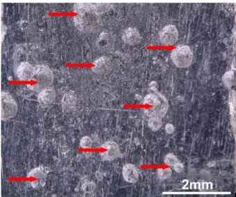
originates the name “tin pest”. Later these ones change into characteristic warts (Fig. 1.). Finally, the tin object can totally disintegrate into powder, which is related to the volume increase [2], and the expansion of the transition into the sample body [3]. Generally, the transition can be divided into 3 phases: nucleation phase when new structure develops via self-organization or a new thermodynamic phase; growth phase when the phenomenon develops; and saturation phase when the transition stops, and β-Sn remains in a metastable state.
Figure 1. Optical image of tin pest warts on the surface of tin object.
Basically, the transition is slow due to a high activation energy. However, several parameters may reduce the time required for the transition e.g., the presence of materials with the same crystal structure, similar lattice parameters to the α-Sn, or the low temperature (<30°C). The tin pest is an autocatalytic reaction, which means the appearance of α-Sn speeds up the transition considerably as well.
Alloying of even small amounts of electropositive metals like Pb, Bi, or Sb suppresses the transition [2], while other insoluble elements, like Zn, Al, Mg, and Mn can significantly accelerate the transition by lowering the activation energy of the transition [4, 5]. Unfortunately, the allotropic transition can occur not only in pure Sn but in high Sn content alloys as well. Nowadays, form economic and environmental reasons, there is a reduction of Ag content in the most widely applied SnAgCu (SAC) solder alloys. In these high Sn content SAC alloys, the Sn content can reach 98 wt%, which could increase the
possibility of different reliability problems, including tin pest phenomenon [6]. The identification and characterization of tin pest in high Sn content solders and surface finishes are crucial for electronic devices working in sub-zero temperatures like aeronautical, aerospace, and automobile applications [6].
At natural conditions, the Sn transition is very slow (can take years) due to a high activation energy of the process [7]. However, as mentioned earlier, the nucleation time can be considerably reduced with the presence of materials that have the same crystallographic parameters. α-Sn itself, InSn, and CdTe are considered as the most effective heterogeneous inoculators. The inoculators are usually applied on the surface of the samples. Nucleation on the surface is much easier and faster than nucleation in the bulk samples. Since the barrier for the nucleation (ΔG*, Gibs free energy) is much lower at the surface than in bulk. However, the application of inoculator materials does not allow the determination of the nucleation time, or to simulate real- life situations, but they are very useful for characterizing the nature of the phenomenon. Besides, CdTe and InSb are widely used in electronic devices. InSb is a promising substrate in high-speed electronics technology and infrared optoelectronics [8] as well as it is used in MOSFET transistor production [9]. CdTe is an alternative material for photovoltaic solar cells [10].
Therefore, both materials can occur at a neighborhood of solder joints and promote tin pest in it.
The tin pest phenomenon results in visible, as well as measurable property, changes in the samples.
Therefore, it can be monitored and characterized by various methods like optical microscopy [6], Scanning Electron Microscopy (SEM) [11], and Focused Ion Beam – Scanning Ionic Microscopy (FIB-SIM) [3]. The amount of the transitioned α-Sn can also be measured with X-Ray diffraction (XRD) [12] and with Mössbauer spectroscopy [13]. It is also possible to investigate tin pest with electrical resistance measurements [14] since the change from metal to semiconductor causes the increase of the electrical resistance. The aim of this work is to determine the obtainable information and limitations in the case of the previous analytical methods, which will be presented with different solder alloys and inoculators as samples.
Acta Materialia Turcica
Volume 4, June 2020, Pages 20-28
2. EXPERIMENTAL PROCEDURE
For the investigation, the samples were prepared from SnCu1 and Sn0.3AgCu0.7 solder alloys. Bulk solder bars were prepared by casting with the sizes:
45x6x3 mm. Heterogeneous inoculation was applied on the surface of the solder bars by InSb, CdTe, and α-Sn powder itself, which was pressed onto the surface by a
mechanic laminator with 30kN force (Fig. 2). Before inoculation, the samples were cleaned in an HCl solution to remove the oxides. Usually, 15-20 samples were produced from each type. The samples were stored at -18
°C for 8-10 weeks (depends on the sample type) in a refrigerator.
Figure 2. The inoculated sample (the inoculator powder is dark gray).
During the test, the surface of the sample was monitored optically by an OLYMPUS BX-52 and HIROX KH-7700 optical microscope and by an FEI Inspect S50 Scanning Electron Microscope (SEM), (Acc.
Voltage 20 kV). The electrical resistance changes of the samples (caused by the ongoing transition) was measured by the 4-wire measurement method with an AGILENT 4338B milliohm meter at room temperature. The measurement accuracy of the instrument at the mΩ range was under 3 %. The repeatability error of the resistance measurements was under 2%. The initial resistance values of the samples were 0.2 - 0.25 mΩ. Cross-sections were also prepared from the samples to investigate the effects of the transition inside the sample body. The cross-sections were studied by an OLYMPUS BX-52 optical microscope.
The α-Sn warts on the surface of the samples were etched with Focused Ion Beam FIB (JEM-9320-FIB) and were observed by Scanning Ion Microscope FIB-SIM (with a Ga ion source and acc. voltage of 30 kV) to study the layer grain structure at tin pest warts. Room- temperature Mössbauer spectra were collected at the tin pest warts to indicate the changes in the ratio of the transitioned and non-transitioned Sn. Renon MsAa-4 spectrometer and gas-filled proportional counter with aluminum cathode were applied. Standard 15 mCi 119Sn source (CaSnO3) supplying γ quanta of energy 23.88 keV
was coupled with the velocity transducer operating in a constant acceleration mode with 5.3 mm/s maximum velocity for periodic Doppler modulation. The Mössbauer spectra were analyzed in the frame of thin absorber approximation (TAA) by a non-linear least square method using Lorentzian lines.
3. RESULTS and DISCUSSION
3.1. Optical and SEM investigations of the β→α-Sn transition
As the α-Sn transition results in visible marks (tin pest warts) on the given objects, the most common way of the investigation is the optical analyses. Fig. 3a shows a typical tin pest wart in the case of α-Sn inoculation. The warts are formed due to the expansion of the α-Sn since it has a higher volume of the unit cell than the β-Sn. The transition process is very similar in each solder alloys and inoculators, but there is a major difference that is determined by the applied inoculator. In the case of α-Sn inoculators, warts start to peel after a while. In the case of InSb or CdTe inoculation, such a peeling is not typical.
However, in the case of InSb and CdTe inoculators, the samples usually decompose at the end of the transition (Fig. 3b), such a decomposition is not typical in the case of α-Sn inoculator.
Acta Materialia Turcica
Volume 4, June 2020, Pages 20-28
Figure 3. Optical images of the tin pest: a) secondary α-Sn warts on the surface of Sn99Cu1 sample inoculated with α-Sn as inoculator; b) decomposed Sn99Cu1 sample inoculated with InSb after 7 weeks of storage at -20°C.
The cause of the sample decompositions is related to the diffusion of the heterogeneous inoculators (InSb or CdTe) from the surface into the sample body. The β→α- Sn transition starts at dozens of places in the whole sample and not only on the surface. Contrary, α-Sn used itself as an inoculator, doesn’t diffuse into the bulk material, and that it is why the transition is located only
at the surface where the inoculator was placed. However, this theory confirmation requires further researches.
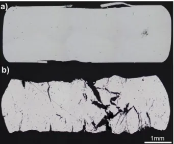
The differences between the samples are even more visible in the metallurgical cross-sections. Fig. 4 shows the cross-sections of Sn99Cu1 samples inoculated with α-Sn (Fig. 4a) and InSb (Fig. 4b) after storage at -20°C for 10 weeks.
Figure 4. Cross-sections of Sn99Cu1 samples after 10 weeks of storage at -20°C: a) α-Sn inoculation; b) InSb inoculation.
In the case of α-Sn inoculator, the peeling of the tin pest warts is clearly visible on the surface of the sample without the expansion of the transition towards the body of the sample. Contrary, in the case of InSb inoculation, the peeling of the warts is not visible, but a large amount
of Sn is transitioned even in the body of the sample.
(Brittle α-Sn is not visible in the photos because it was falling out from the sample during polishing).
Acta Materialia Turcica
Volume 4, June 2020, Pages 20-28
The deformation of the grains during the transition (the cracks due to the sliding of the grains) is clearly visible on SEM micrographs (Fig. 5), as well as the
indentation of the inoculator materials into the surface of the samples. The indentation of the inoculator material into the sample body is essential due to the fast nucleation of the α-Sn transition.
Figure 5. SEM micrograph of a tin pest warts growth on Sn99Cu1 inoculated with InSb after 8 weeks of storage at -20°C.
3.2. Electrical resistance changes measurements during β→α-Sn transition
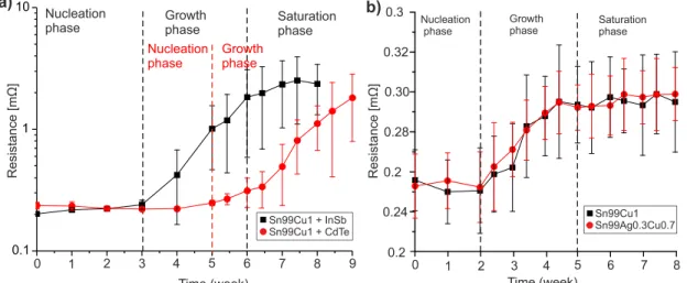
Fig. 6a shows the electrical resistance change of Sn99Cu1 samples inoculated with InSb and CdTe on a logarithmic scale. In the first 3 weeks of the tests, the resistance change was negligible, and it was in the range of the repeatability and measurement error. However, some tin pest warts already appeared after 2 weeks of storage at -20 °C. After 3 weeks, all samples showed 5–
20 % of resistance increase, therefore the nucleation phase of the α-Sn transition was determined to be 3 weeks. In the period 3–6 week (the growth phase), a considerable increase of electrical resistance was detected with a high deviation (±0.25mΩ at 4th week and
±3mΩ at 6th week). The high deviation can be caused by the combined effect of the not totally even inoculation, and the autocatalytic nature of the α-Sn transition. The differences in the appearance and in the amount of α-Sn result in considerable differences in the transition rates.
After 6 weeks of storage at -20°C, the electrical resistance increase reached the saturation phase (Fig. 6a).
After 8 weeks, the sample bodies started to decompose into powder and bigger sized pieces, so the test was terminated since it was not possible to carry it further.
The decomposition of the sample bodies usually
occurred when the electrical resistance had increased by 25–30 times. The highest resistance increase for these samples was ~33 times (to 8.3mΩ) after 8 weeks of storage at -20 °C.
In the case of Sn99Cu1 samples inoculated with CdTe, the nucleation phase was longer, the first tin pest warts appeared only after 4 weeks, and the resistance increase started only after 5 weeks of storage at 20 °C.
So, the nucleation phase was 5 weeks at these samples.
After 5 weeks, a considerable increase of the electrical resistance occurred without the reach of saturation till the end of the 8th week. These observations match with the results of Di Maio and Hunt. They neither found saturation phases in the electrical resistance changes of different SnCu and SnAg alloys inoculated with CdTe at -35 °C [14]. After 8 weeks, the sample bodies started to decompose, and the test was terminated. Here, the deviation of the resistance increase was smaller than in the case of InSb inoculator (±0.027mΩ at 6th week and
±1.15mΩ at 8th week). The highest resistance increase for the samples was ~32 times (to 8.13mΩ) after 8 weeks of storage at -20 °C.
In the case of α-Sn inoculator, the Sn99Cu1 and Sn99Ag0.3Cu0.7 alloys showed similar behavior (Fig.
6b). The nucleation phase was shorter than in the
Acta Materialia Turcica
Volume 4, June 2020, Pages 20-28
previous cases, the first tin pest warts already appeared only after 2 weeks of storage at -20ºC. After 2 weeks, 10- 15% of electrical resistance increases were detected, and it was still continuing the 5th week. At these samples, the decomposition of the sample bodies was not observed at all. As it was discussed in Section 3.1, in the case of α- Sn inoculator, the transition cannot develop into the body of the samples, and it is limited mostly to the sample
surface. Due to the slight change of the electrical resistance, the deviation was generally low, and even during the whole study (±0.015-0.020mΩ). The samples Sn99Ag0.3Cu0.7 alloy inoculated with InSb and CdTe were totally resistant to α-Sn transition. They showed no tin pest signs or electrical resistance change still after 8 weeks of storage at 20ºC.
Figure 6. Electrical resistance changes of the samples after 8 weeks of storage at -20°C: a) Sn99Cu1 inoculated with InSb and CdTe; b) Sn99Cu1 and Sn99Ag0.3Cu0.7 inoculated with α-Sn.
The electrical resistance measurement can be an effective method for tin pest detection and characterization as well. The range of this method is high, from ~10 to 3000% resistance change is detectable, and the process can be followed until the total disintegration of the samples. Besides, the nature of transition (the different phases in the case of different alloys and inoculators) can be easily distinguished with the measurement of the electrical resistance changes.
3.3. FIB-SIM and Mössbauer spectroscopy studies
of β→α-Sn transition
As it was discussed earlier, the transition cannot cover all β-Sn grains. It usually stops after a while (saturation phase of the transition), even if the samples are still subjected to the low temperature. The root caused of this interesting phenomenon can be investigated with more sophisticated methods like the FIB-SIM and the Mössbauer spectroscopy.
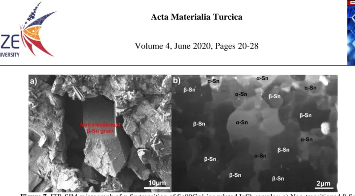
Non-transitioned β-Sn grains were found even on the surface of the samples by FIB-SIM (Fig. 7a). The transition took place around a single crystalline β-Sn grain, but the grain itself remained non-transitioned. The brittle α-Sn is already missing around the non- transitioned β-Sn grain. Fig. 7b shows a FIB cross- section performed at a transitioned area of the sample.
Acta Materialia Turcica
Volume 4, June 2020, Pages 20-28
Figure 7. FIB-SIM micrograph of α-Sn transition of Sn99Cu1 inoculated InSb samples: a) Non-transitioned β-Sn grain on the surface of a; b) vertical expansion of α-Sn into β-Sn grains.
The different phases of Sn can be determined by X- ray diffraction (XRD) measurements, however, the transitioned grains can be distinguished easily according to the sizes and contrast difference between the β and α- Sn grains [7]. Fig. 7b confirms that not all the β-Sn grains transformed to α-Sn. Even the hypothetically completely transitioned areas can contain non-transitioned β-Sn grains (like the right upper corner of the micrograph).
Besides, the rapid vertical expansion of the tin pest into the sample body in the case of InSb inoculation is also clearly visible in Fig. 7b.
It can also occur that the newly developed α-Sn grains enclose non-transitioned β-Sn grains and inhibit the further transition (and results in that β-Sn grains remain in a metastable state). This phenomenon might be caused by the considerable volume increase (of 27%) of a single unit cell of α-Sn as compared to β-Sn. This increase causes an increase in mechanical stress and local
pressure. The Gibbs free energy (G), ensuring the thermodynamic equilibrium of Sn phases (α and β-Sn) is strongly influenced by pressure value. If the value of the pressure is changed locally, the thermodynamic equilibrium is also shifted locally.
The ratio of the transitioned and non-transitioned Sn can be determined by Mössbauer spectroscopy. Fig. 8 shows the Mössbauer spectra of Sn99Cu1 and Sn99Ag0.3Cu0.7 alloys inoculated with InSb after the saturation phase of the process. In the case of the Sn99Cu1 alloy (Fig. 8a), the ratio of both Sn phases was found near equal. It was an interesting result considering that the investigated samples were already a fine grey powder at the time investigation. This finding proves that even in highly decomposed samples (e.g. powder look like), β-Sn is still present, although one can assume that the transition is finished, and the dominant form should be pure α-Sn.
Acta Materialia Turcica
Volume 4, June 2020, Pages 20-28
Figure 8. Mössbauer spectra: a) Sn99Cu1 inoculated with InSb; b) Sn99Ag0.3Cu0.7 inoculated with InSb [15].
In the case of the Sn99Ag0.3Cu0.7 alloy (Fig. 8b), only a small amount of α-Sn was detected, as it was expected according to the electrical resistance measurements as well (Fig. 6c). It proves that the Ag additive to the alloy, even at a low level, is a successful suppressor of the α-Sn transition [15].
4. CONCLUSION
Different analytical methods were applied to characterize the tin pest phenomenon in the case of different solder alloys and inoculator materials. With the application of metallurgical cross-sections and metal microscopy, the development of the process can be characterized in the case of different inoculator materials.
It was found that in the case of α-Sn inoculator, the transition develops on the surface of the samples. In contrary in the case of InSb or CdTe inoculators, the transition develops towards the body of the sample which leads to the decomposition of the samples. The electrical resistance measurement is very useful to characterize the different phases of the transition in the case of different alloys and inoculator materials, like nucleation, growth, and saturation phases. It was found that in the case of the CdTe inoculator, the saturation phase of the process is not detectable, and the Ag additive suppresses the transition very effectively. The SEM and FIB-SIM investigations can provide information about the change of the microstructure during the transition, like the grain sliding and secondary α -Sn expansion in time. The Mössbauer spectroscopy provides information about the amount of the transitioned Sn and about the duration of the transition process. Therefore, the accurate characterization of the β→α-Sn transition in the given
material combinations is possible only with the combined application of the investigated analytical methods.
5. ACKNOWLEDGMENT
This research was partially supported by the Higher Education Excellence Program of the Ministry of Human Capacities in the frame of Nanotechnology and Materials Science research area of Budapest University of Technology and Economics (BME FIKP-NAT) and by the National Research, Development and Innovation Office – NKFIH, FK 127970.
6. REFERENCES
[1] A. M. Molodets, S. S. Nabatov, Thermodynamic Potentials, Diagram of State, and Phase Transitions of Tin on Shock Compression, High Temp. 38/5 (2000) 715-721. DOI: 10.1007/BF02755923
[2] A. Skwarek, P. Zachariasz, J. Kulawik, K. Witek, Inoculator dependent induced growth of α-Sn, Materials Chemistry and Physics 166 (2015) 16-19. DOI:
10.1016/j.matchemphys.2015.09.017
[3] A. Skwarek, B. Illés, B. Horváth, A. Géczy, P Zachariasz, D. Bušek, Identification and caracterization of ß→α-Sn transition in SnCu1 bulk alloy inoculated with InSb, J. Mater. Sci. Mater. Electron. 28 (2017) 16329–16335. DOI: 10.1007/s10854-017-7539-5
Acta Materialia Turcica
Volume 4, June 2020, Pages 20-28
[4] M. Leodolter-Dworak, I. Stefan, W.J. Plumbridge, H.
Ipser, Tin Pest in Sn-0.5Cu Lead-Free Solder Alloys: A Chemical Analysis of Trace Elements, J. Electron.
Mater. 39/1 (2010) 105-108. DOI: 10.1007/s11664-009- 0958-1
[5] D. Giuranno, S. Delsante, G. Borzone, R. Novakovic, Effects of Sb addition on the properties of Sn-Ag- Cu/(Cu, Ni) solder systems, J. Alloys Compds 689 (2016) 918-930. DOI: 10.1016/j.jallcom.2016.08.035 [6] A. Skwarek, M. Sroda, M. Pluska, A. Czerwinski, J.
Ratajczak, K. Witek, Occurrence of tin pest on the surface of tin-rich lead-free alloys, Solder. Surf. Mount
Tech. 23/3 (2011) 184-190. DOI:
10.1108/09540911111146944
[7] W.J. Plumbridge, Tin pest issues in lead-free electronic solders, J. Mater. Sci. – Mater. Electron. 18 (2007) 307-318.
DOI: 10.1007/978-0-387-48433-4_20
[8] K. Zhang, Y. Wang, W. Jin, X. Fang, Y. Wan, Y.
Zhang, L. Dai, High-quality InSb nanocrystals: synthesis and application in graphene-based near-infrared photodetectors, RSC Adv. 6/30 (2016) 25123-25127.
DOI: 10.1039/C6RA00503A
[9] T. Ito, A. Kadoda, K. Nakayama, Y. Yasui, M. Mori, K. Maezawa, T. Mizutani, Effective mobility enhancement in Al2O3/InSb/Si quantum well metal oxide semiconductor field effect transistors for thin InSb channel layers, Jpn. J. App. Phys. 52/4S (2013) 04CF01.
DOI: 10.7567/JJAP.52.04CF01
[10] A.Y. Shenouda, M.M. Rashad, L. Chow, Synthesis, 10haracterization and performance of Cd 1− xInxTe compound for solar cell applications, J. Alloys Compds.
563 (2013) 39-43. DOI: 10.1016/j.jallcom.2013.02.076
[11] N. D. Burns, A Tin Pest Failure, J. Failure Anal.
Prev. 9/5 (2009) 461-465. DOI: 10.1007/s11668-009- 9280-8
[12] K. Nogita, C.M. Gourlay, S.D. McDonald, S.
Suenaga, J. Read, G. Zeng, Q.F. Gud, XRD study of the kinetics of β↔α transformations in tin, Phil. Mag. 93/27
(2013) 3627-3647. DOI:
10.1080/14786435.2013.820381
[13] A. Skwarek, P. Zachariasz, J. Zukrowski, B.
Synkiewicz, K. Witek, Early stage detection of ß → α a transition in Sn by Mössbauer spectroscopy, Mater.
Chem. Phy. 182 (2016) 10-14.
DOI: 10.1016/j.matchemphys.2016.07.061
[14] D. Di Maio, C.P. Hunt, Monitoring the Growth of the α Phase in Tin Alloys by Electrical Resistance Measurements, J. Electron. Mater. 38/9 (2009) 1874- 1880. DOI: 10.1007/s11664-009-0822-3
[15] A. Skwarek, P. Zachariasz, B. Illés, J. Żukrowski, T.
Hurtony, K. Witek, Mössbauer studies of f ß→α phase transition in Sn-rich solder alloys, Microelectron. Reliab.
82 (2018) 165-170.
DOI: 10.1016/j.microrel.2018.01.016


![Figure 8. Mössbauer spectra: a) Sn99Cu1 inoculated with InSb; b) Sn99Ag0.3Cu0.7 inoculated with InSb [15].](https://thumb-eu.123doks.com/thumbv2/9dokorg/791985.37148/8.918.61.817.60.447/figure-mössbauer-spectra-sn-inoculated-insb-inoculated-insb.webp)
