coatings
Article
Transformations in CrFeCoNiCu High Entropy Alloy Thin Films during In-Situ Annealing in TEM
Mohamed Arfaoui1,2,*, György Radnóczi1 and Viktória Kovács Kis1,3
1 Centre for Energy Research of the Hungarian Academy of Sciences, Konkoly-Thege M. u.
29-33, H-1121 Budapest, Hungary; radnoczi.gyorgy@energia.mta.hu (G.R.);
kis.viktoria@energia.mta.hu (V.K.K.)
2 Deptartment of Physics, Eötvös Loránd University, Pázmány Péter sétány 1a, H-1117 Budapest, Hungary
3 Institute of Environmental Sciences, University of Pannonia, Egyetem str. 10, H-8200 Veszprém, Hungary
* Correspondence: Mohamed.arfaoui@mfa.kfki.hu; Tel.:+36-70-244-3026
Received: 13 December 2019; Accepted: 7 January 2020; Published: 9 January 2020
Abstract:In-situ TEM-heating study of the microstructural evolution of CrFeCoNiCu high entropy alloy (HEA) thin films was carried out and morphological and phase changes were recorded.
Post annealing investigation of the samples was carried out by high resolution electron microscopy and EDS measurements. The film is structurally and morphologically stable single phase FCC HEA up to 400◦C. At 450◦C the formation of a BCC phase was observed, however, the morphology of the film remained unchanged. This type of transformation is attributed to diffusionless processes (martensitic or massive). From 550◦C fast morphological and structural changes occur, controlled by volume diffusion processes. Fast growing of a new intermetallic phase is observed which contains mainly Cr and has large unit cell due to chemical ordering of components in<100>direction. The surface of the films gets covered with a CrO-type layer, possibly contributing to corrosion resistance of these.
Keywords: high entropy alloy; in-situ TEM annealing; thermal stability; diffusionless transformation;
planar disorder; oxide formation
1. Introduction
High entropy alloys (HEAs) are multi-component alloys in which at least five elements of concentration between 5 and 30 at % are combined [1]. The basic idea is to reduce the Gibbs free energy through maximizing the configuration entropy, which facilitates the formation of random solid solution rather than a complex microstructure built up by intermetallic compounds [2,3]. Thus, studying the structure and stability of HEA during high temperature treatments [4–6] both at the micro- and atomic levels, is a critical issue in understanding of their growth processes.
Detailed structural investigations of bulk HEA have shown that some ordered solid solutions as well as intermetallic compounds can precipitate from the homogeneous matrix at room temperature (RT) and at elevated temperatures as well. For example, ordered FCC phases were found at RT in the Al0.5CoCrCuFeNi [7] and Al0.3CoCrFeNi [8] as well disordered BCC and ordered B2 phases in Al0.5CoCrCuFeNi [9] and AlxCoCrFeNi [10]. The size and the lattice parameter of these BCC grains have been found to be of the order of ten micrometers and 0.289 nm respectively, regardless of their composition.
Several studies deal with structural changes in HEAs at elevated temperatures. The CrFeMnCoNi alloy, considered as a stable HEA at temperatures below its melting point, formed both carbide and σphase at grain boundaries of the FCC matrix after prolonged exposures to 700◦C [11]. Recent investigations show that in the same material three different phases (L10-NiMn, B2-FeCo and a Cr-rich body-centered cubic, BCC phase) can precipitate at the grain boundaries after long time annealing
Coatings2020,10, 60; doi:10.3390/coatings10010060 www.mdpi.com/journal/coatings
in the 500–900◦C temperature interval [12]. With a minor addition of Al to CrFeCoNi HEA it also became unstable leading to the formation of a Cr-rich phase after a long time annealing at 750◦C [13].
The formation ofσphase is reported after annealing at 1000◦C for 15 min of the CrCuCoFeNi alloy as well [14]. Synchrotron XRD results [15,16] show that the microstructure at RT of bulk as-cast CrFeCoNiCu alloy exhibits two FCC phases of lattice constants 0.361 nm and 0.358 nm. One of these phases is Cu-poor with dendritic morphology and the other is a Cu-rich interdendritic phase. Moreover, the two-phase structure is preserved even after a heat treatment at 1100◦C and 1250◦C and, in parallel, the Cu content of the interdendritic region increased [17,18].
Most of these results were obtained with the aim of understanding structural changes within the as cast or homogenized HEA at elevated temperatures, and indicate that the effect of sluggish cooperative diffusion and negative mixing entropy of elements, which inhibits the growth of new phases and nanoparticles at low temperatures, diminishes under heat treatment.
Based on these experimental results, scientific attention has been focused on the application of HEAs as thin film materials. Due to the higher cooling rate and vapor-solid formation mechanism [15], these films can provide different (nano) structural properties compared to bulk HEA. The Al0.5CrFeCoNiCu [19] thin film reported by Chen et al. in 2004 showed a FCC single solid solution based on X-ray diffraction. According to TEM, the CrFeCoNiCu (200 nm thick HEA thin film) grows in face centered cubic solid solution and no obvious Cu segregation was observed even on the nanometer scale [15,20]. This supports the great potential of the sputtering technique to produce uniform elemental distribution leading to single phase nanostructure due to fast quenching rate as compared to the as-cast samples.
Regarding structural changes of HEA thin films at elevated temperatures only a few in-situ experiments have been published. For example, in-situ X-ray diffraction studies were carried out on 1µm thick AlCoCrCuFeNi thin films in the temperature range 110–810◦C by Dolique et al. [21].
They found that AlCoCrCuFeNi films were stable up to 510◦C, which indicates an inferior thermal stability to their bulk counterpart (800◦C). The effect of Al on thermal behavior of AlxCoCrFeNi film was investigated by in-situ TEM heat treatment at 500◦C and 900◦C as well [22]. The results clearly confirmed that increasing the Al content initiates the formation of B2/BCC phases, which are precursors of a sigma phase.
The in-situ in TEM heating and electron irradiation experiment of a 100 nm thick sputtered CrFeCoNiCu HEA thin film in the temperature range 20–720◦C [23] also supports the formation of BCC/B2 phases at 300◦C, which is followed by sigma phase formation at 720◦C. However, a recent, in-situ TEM heating of the same polycrystalline alloy confirmed microstructure stabilization up to 300◦C during 1800 s [24]. On the other hand, it is also known, that the atomic structure (FCC or BCC or both phases) in these alloys play a sensitive role in the mechanical properties [16,18] as well in the nucleation pathway of the sigma phase [10,22,23]. At the same time, the early stages of phase evolution and transformation mechanisms leading to the formation of ordered intermetallic phases (e.g., L12, B1, and sigma) at intermediate and elevated temperatures in multicomponent films are still not revealed in details.
The present work is motivated by the need for a better understanding and controlling the initial stages of phase and compositional instability of as deposited CrFeCoNiCu HEA thin films with increasing temperature. To achieve this goal in-situ TEM-heating study of the microstructural evolution of CrFeCoNiCu thin film is carried out at intermediate and elevated temperatures up to 700◦C to record the morphological and phase changes from as early stages as possible.
2. Materials and Methods
CrFeCoNiCu high entropy (HEA) films were deposited in a high vacuum system by direct current magnetron sputtering. Films with a thickness of 50 nm were grown at room temperature on cleaved NaCl substrate coated with about 5 nm SiOxlayer as well as on 30 nm thick amorphous SiOxfilm substrate supported by Cu micro-grids. The substrates were placed at a distance of 120 mm from
Coatings2020,10, 60 3 of 15
the target in the centre of the rotating substrate holder. The equiatomic concentration arc melted CrFeCoNiCu target of 99.95%, purity was mounted 25◦toward the vertical. The background pressure of the deposition system was 9×10⁻⁶Pa. High purity Ar was used as sputtering gas at a pressure of 0.25 Pa. The target was pre-sputtered for 5 min before deposition with the shutter closed. The DC power and the deposition time were set to 50 W and 5 min respectively resulting in a 50 nm thick film.
The films grown on the NaCl/SiOxsubstrate were floated offfrom NaCl and placed on a micro grid.
The in-situ annealing was carried out in a Philips CM20 transmission electron microscope, operated at 200 keV. The temperature was raised in steps of 50◦C from room temperature up to 700◦C, having the temperature constant at each step for 5 min. The vacuum in the microscope specimen area was maintained at 4.5×10⁻⁵Pa during the whole in-situ annealing process.
Two kinds of in-situ annealing experiments were carried out. First, the changes were followed by selected area diffraction (SAED), recording diffraction patterns from the same area of 1µm in diameter at the end of each temperature step. For the evaluation of the SAED patterns, the camera constant was calibrated using a 50 nm thick self-supporting random nanocrystalline Al thin film.
In the second case bright field (BF) images were recorded at magnification of 50,000×at the end of each temperature step. The experiments were performed in the way to ensure the observation of changes preferably in the same area of the film. In both in-situ runs (SAED and BF), the sample was quenched to room temperature after having it hold at 700◦C for 5 min.
Energy dispersive X-ray spectroscopy (EDS) (Themis 200 G3 Super-X EDS detector, Eindhoven, The Netherlands) analysis was performed to verify the composition of the samples before and after annealing. Further structural and EDS characterization of the 700◦C annealed sample was carried out by a FEI-Themis transmission electron microscope (Themis 200 G3, Eindhoven, The Netherlands) with a Cs corrected objective lens, in both HREM (High Resolution Electron Microscope) and STEM (Scanning Transmission Electron Microscope) mode (point resolution is around 0.09 nm in HREM mode and 0.16 nm in STEM mode) operated at 200 kV.
3. Results
3.1. Morphology and Diffraction Analysis of the Film during Heating
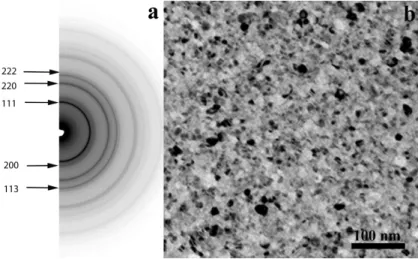
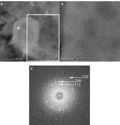
As can be seen in Figure1, the electron diffraction pattern of the as-deposited film indicates the presence of a single FCC solid solution phase while the image shows a fine-grained microstructure of about 5–10 nm average grain size. The crystallographic orientation of the grains is random as verified by tilting experiments: the intensity distribution along the diffraction rings does not change up to 35◦ of tilt angle. By averaging the lattice constants from all measurable FCC rings, the size of the unit cell of the FCC-phase is calculated to be 0.360 nm, very close to that of pure FCC Cu, and is in agreement with values published for the same alloy in literature [15,20,23].
The initial processes taking place during in-situ annealing are the target of the present investigations.
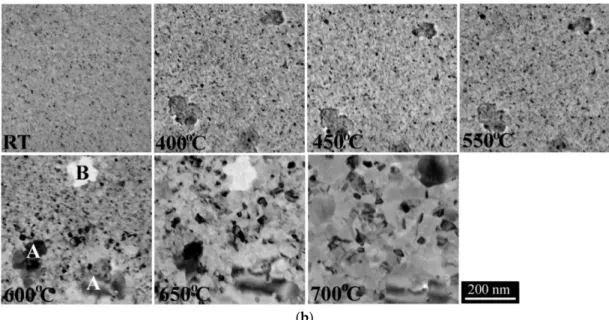
Selected stages of the transformation of the CrFeCoNiCu film as followed by SAED and TEM bright field (BF) images are shown in Figure2.
From the analysis of the SAED patterns (Figures1a and2a) we conclude that up to 400◦C only the as grown FCC phase could be observed, and accordingly, BF images (Figure2b) indicate that the same polycrystalline structure with a grain size about 5–10 nm was preserved. Thus, it could be concluded that the film was structurally stable up to 400◦C.
At 450◦C a new diffraction ring appears in the electron diffraction pattern. Careful analysis of the SAED pattern allowed identifying further diffraction rings which correspond to a BCC phase of lattice parameter aBCC=0.294±0.010 nm. So, we could conclude that at 450◦C the CrFeCoNiCu HEA film had a two-phase structure, composed from the original FCC and the newly formed BCC phase.
It is important to note that these two lattices were related to each other by fulfilling the following relation: d(111)FCC=d(110)BCC, i.e., the lattice spacing of the {111} planes in the FCC phase was equal
to the lattice spacing of the {110} planes of the BCC phase. No morphological changes were detectable;
also the BCC grains could not be identified based on their morphology.
Coatings 2020, 10, x FOR PEER REVIEW 4 of 15
Figure 1. Electron diffraction pattern (a) and bright field TEM image (b) of the as-deposited CrFeCoNiCu high entropy alloy (HEA) film. The electron diffraction pattern indicates a single phase FCC structure.
The initial processes taking place during in-situ annealing are the target of the present investigations. Selected stages of the transformation of the CrFeCoNiCu film as followed by SAED and TEM bright field (BF) images are shown in Figure 2.
From the analysis of the SAED patterns (Figures 1a and 2a) we conclude that up to 400 °C only the as grown FCC phase could be observed, and accordingly, BF images (Figure 2b) indicate that the same polycrystalline structure with a grain size about 5–10 nm was preserved. Thus, it could be concluded that the film was structurally stable up to 400 °C.
(a)
Figure 1.Electron diffraction pattern (a) and bright field TEM image (b) of the as-deposited CrFeCoNiCu high entropy alloy (HEA) film. The electron diffraction pattern indicates a single phase FCC structure.
Upon further heating, up to 550◦C a few grains with somewhat larger size appear randomly distributed over all of the film area. The diffraction rings of the FCC host phase show texture-like redistribution manifested by the appearance of higher intensity arcs on the rings. At this temperature only the original FCC HEA phase changes, no similar texture-like redistribution was observed in the diffraction rings of the BCC phase.
At 600◦C a drastic change in the microstructure occurs. New grains with larger size appear as marked by A in Figure2b and grow rapidly to a size of several 100 nm at the expense of the existing two-phase matrix. These grains must belong to the already existing BCC phase as the diffraction rings belonging to the BCC phase (Figure2a, 600◦C) became discontinuous, indicating grain size growth and, consequently, fewer and larger BCC grains in the same selected area. Nevertheless, at 600◦C the diffraction pattern contains only the FCC and BCC reflections, i.e., no new phases formed. On the other hand, also at this temperature a redistribution of the film material could be observed. Thin, apparently void-like areas formed and grew in the FCC–BCC matrix (B in Figure2b).
Coatings 2020, 10, x FOR PEER REVIEW 4 of 15
Figure 1. Electron diffraction pattern (a) and bright field TEM image (b) of the as-deposited CrFeCoNiCu high entropy alloy (HEA) film. The electron diffraction pattern indicates a single phase FCC structure.
The initial processes taking place during in-situ annealing are the target of the present investigations. Selected stages of the transformation of the CrFeCoNiCu film as followed by SAED and TEM bright field (BF) images are shown in Figure 2.
From the analysis of the SAED patterns (Figures 1a and 2a) we conclude that up to 400 °C only the as grown FCC phase could be observed, and accordingly, BF images (Figure 2b) indicate that the same polycrystalline structure with a grain size about 5–10 nm was preserved. Thus, it could be concluded that the film was structurally stable up to 400 °C.
(a) Figure 2.Cont.
Coatings2020,10, 60 5 of 15
Coatings 2020, 10, x FOR PEER REVIEW 5 of 15
(b)
Figure 2. Diffraction patterns (a) and in-situ TEM bright field images (b) recorded at temperatures marked in individual images.
At 450 °C a new diffraction ring appears in the electron diffraction pattern. Careful analysis of the SAED pattern allowed identifying further diffraction rings which correspond to a BCC phase of lattice parameter aBCC = 0.294 ± 0.010 nm. So, we could conclude that at 450 °C the CrFeCoNiCu HEA film had a two-phase structure, composed from the original FCC and the newly formed BCC phase.
It is important to note that these two lattices were related to each other by fulfilling the following relation: d(111)FCC = d(110)BCC, i.e., the lattice spacing of the {111} planes in the FCC phase was equal to the lattice spacing of the {110} planes of the BCC phase. No morphological changes were detectable;
also the BCC grains could not be identified based on their morphology.
Upon further heating, up to 550 °C a few grains with somewhat larger size appear randomly distributed over all of the film area. The diffraction rings of the FCC host phase show texture-like redistribution manifested by the appearance of higher intensity arcs on the rings. At this temperature only the original FCC HEA phase changes, no similar texture-like redistribution was observed in the diffraction rings of the BCC phase.
At 600 °C a drastic change in the microstructure occurs. New grains with larger size appear as marked by A in Figure 2b and grow rapidly to a size of several 100 nm at the expense of the existing two-phase matrix. These grains must belong to the already existing BCC phase as the diffraction rings belonging to the BCC phase (Figure 2a, 600 °C) became discontinuous, indicating grain size growth and, consequently, fewer and larger BCC grains in the same selected area. Nevertheless, at 600 °C the diffraction pattern contains only the FCC and BCC reflections, i.e., no new phases formed. On the other hand, also at this temperature a redistribution of the film material could be observed. Thin, apparently void-like areas formed and grew in the FCC–BCC matrix (B in Figure 2b).
The number of the large grains increased further at 650 °C (Figure 2b and Figure 3). In agreement with this observation the BCC rings in the diffraction pattern contained more and stronger spots.
Some growth of the matrix (FCC) grains could also be concluded from Figure 2b, however, the FCC rings in the diffraction pattern (Figure 2a, 650 °C) remained continuous, indicating only minor changes. In addition, many new reflections appeared including a diffraction ring at 0.25 nm (marked by arrows in Figure 2a).
Figure 2.Diffraction patterns (a) and in-situ TEM bright field images (b) recorded at temperatures marked in individual images.
The number of the large grains increased further at 650◦C (Figures2b and3). In agreement with this observation the BCC rings in the diffraction pattern contained more and stronger spots.
Some growth of the matrix (FCC) grains could also be concluded from Figure2b, however, the FCC rings in the diffraction pattern (Figure2a, 650◦C) remained continuous, indicating only minor changes.
In addition, many new reflections appeared including a diffraction ring at 0.25 nm (marked by arrows in Figure2a).
Coatings 2020, 10, x FOR PEER REVIEW 6 of 15
Figure 3. (a) Bright field (BF0 TEM image and (b) selected area diffraction (SAED) pattern of a 1µm in diameter area (b) of the HEA film, recorded at 700 °C.
At 700 °C the scattered reflections already observed at 650 °C increase in number and strength and the diffraction rings of the BCC phase (a = 0.294 nm) became even less continuous though still can be distinguished. This observation implies further grain growth of the A type grains (BCC phase) in the 650–700 °C temperature interval (Figures 2 and 3). On the other hand, the diffraction rings of the FCC phase became also spotted (Figure 3), indicating a grain growth or/and decrease in number of the FCC grains. As a result, the film had a bimodal grain size distribution (Figure 3a). The grains of the matrix phases (mainly FCC) and the large grains (A in Figure 3a) were present having a grain size of 20–50 nm and of about a few hundred nm, respectively.
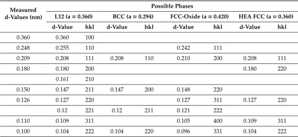
According to the phase analysis of the diffraction pattern recorded at 700 °C (Figure 3b) the L12 simple cubic phase reflections of the same lattice parameter as the host HEA FCC phase (a = 0.360 nm) were identified besides of the BCC phase (a = 0.294 nm). Moreover, another small grain size FCC phase of a = 0.420 nm was present, which could be identified as a complex oxide phase [25].
The measured and calculated lattice spacing values of the identified phases are summarized in Table 1. As seen from Table 1, there were a lot of overlaps between lattice distances of the four identified phases.
Table 1. Lattice distances of phases measured in the HEA film after annealing at 700 °C for 5 min (Figure 3) and calculated values for the expected phases.
Measured d-Values (nm)
Possible Phases
L12 (a = 0.360) BCC (a = 0.294) FCC-Oxide (a = 0.420)
HEA FCC (a = 0.360) d-Value hkl d-Value hkl d-Value hkl d-Value hkl
0.360 0.360 100
0.248 0.255 110 0.242 111
0.209 0.208 111 0.208 110 0.210 200 0.208 111
0.180 0.180 200 0.180 220
0.161 210
0.150 0.147 211 0.147 200 0.148 220
0.126 0.127 220 0.127 311 0.127 220
0.12 221 0.12 211 0.121 222
0.110 0.109 311 0.105 400 0.109 311
0.100 0.104 222 0.104 220 0.096 331 0.104 222
Figure 3.(a) Bright field (BF0 TEM image and (b) selected area diffraction (SAED) pattern of a 1µm in diameter area (b) of the HEA film, recorded at 700◦C.
At 700◦C the scattered reflections already observed at 650◦C increase in number and strength and the diffraction rings of the BCC phase (a=0.294 nm) became even less continuous though still can be distinguished. This observation implies further grain growth of the A type grains (BCC phase) in the 650–700◦C temperature interval (Figures2and3). On the other hand, the diffraction rings of the FCC phase became also spotted (Figure3), indicating a grain growth or/and decrease in number of the FCC grains. As a result, the film had a bimodal grain size distribution (Figure3a). The grains of the
matrix phases (mainly FCC) and the large grains (A in Figure3a) were present having a grain size of 20–50 nm and of about a few hundred nm, respectively.
According to the phase analysis of the diffraction pattern recorded at 700 ◦C (Figure3b) the L12 simple cubic phase reflections of the same lattice parameter as the host HEA FCC phase (a=0.360 nm) were identified besides of the BCC phase (a=0.294 nm). Moreover, another small grain size FCC phase of a=0.420 nm was present, which could be identified as a complex oxide phase [25].
The measured and calculated lattice spacing values of the identified phases are summarized in Table1. As seen from Table1, there were a lot of overlaps between lattice distances of the four identified phases.
Table 1. Lattice distances of phases measured in the HEA film after annealing at 700◦C for 5 min (Figure3) and calculated values for the expected phases.
Measured d-Values (nm)
Possible Phases
L12 (a=0.360) BCC (a=0.294) FCC-Oxide (a=0.420) HEA FCC (a=0.360)
d-Value hkl d-Value hkl d-Value hkl d-Value hkl
0.360 0.360 100
0.248 0.255 110 0.242 111
0.209 0.208 111 0.208 110 0.210 200 0.208 111
0.180 0.180 200 0.180 220
0.161 210
0.150 0.147 211 0.147 200 0.148 220
0.126 0.127 220 0.127 311 0.127 220
0.12 221 0.12 211 0.121 222
0.110 0.109 311 0.105 400 0.109 311
0.100 0.104 222 0.104 220 0.096 331 0.104 222
The textured reflections we considered to belong to the FCC and L12 phases. In this diffraction pattern the BCC phase could not be clearly observed, its scattered reflections became hardly visible in the 650–700◦C temperature interval, the overlaps with the FCC and L12 phases were evident (Table1).
All the rings especially at larger d values were composed of reflections belonging to slightly different spacings. This could be due to composition and consequently lattice parameter fluctuations in the alloy. Nevertheless, the diffraction patterns in Figure2a unambiguously show, that the 0.150 nm ring cannot belonged to the BCC and L12 phases only, as at 700◦C it reappeared and it was composed from much smaller grains than the L12 and BCC phases had (continuous ring versus spotty rings). So, together with the 0.248 nm ring, which had the same character, the 0.150 nm ring must belong to the FCC oxide phase, the small grain nature of which would be seen in the HREM images below.
3.2. Microstructure Analysis of the Film Annealed at 700◦C
A detailed high resolution structure and composition analysis of the film, formed during in-situ annealing to 700◦C was carried out in a FEI Titan-Themis microscope at room temperature.
The High Angle Angular Dark Field (HAADF) image and elemental maps of the annealed film are shown in Figures4and5. Figure4shows grains with dark gray contrast having the lowest average Z in their composition. These grains correspond to dark grains marked A in Figure2b (600◦C) and 3 as well as in Figure4. These grains, formed in the temperature range between 600 and 700◦C were embedded in a lighter matrix of higher Z.
Coatings2020,10, 60 7 of 15
Coatings 2020, 10, x FOR PEER REVIEW 7 of 15
The textured reflections we considered to belong to the FCC and L12 phases. In this diffraction pattern the BCC phase could not be clearly observed, its scattered reflections became hardly visible in the 650–700 °C temperature interval, the overlaps with the FCC and L12 phases were evident (Table 1). All the rings especially at larger d values were composed of reflections belonging to slightly different spacings. This could be due to composition and consequently lattice parameter fluctuations in the alloy. Nevertheless, the diffraction patterns in Figure 2a unambiguously show, that the 0.150 nm ring cannot belonged to the BCC and L12 phases only, as at 700 °C it reappeared and it was composed from much smaller grains than the L12 and BCC phases had (continuous ring versus spotty rings). So, together with the 0.248 nm ring, which had the same character, the 0.150 nm ring must belong to the FCC oxide phase, the small grain nature of which would be seen in the HREM images below.
3.2. Microstructure Analysis of the Film Annealed at 700 °C
A detailed high resolution structure and composition analysis of the film, formed during in-situ annealing to 700 °C was carried out in a FEI Titan-Themis microscope at room temperature.
The High Angle Angular Dark Field (HAADF) image and elemental maps of the annealed film are shown in Figures 4 and 5. Figure 4 shows grains with dark gray contrast having the lowest average Z in their composition. These grains correspond to dark grains marked A in Figure 2b (600
°C) and 3 as well as in Figure 4. These grains, formed in the temperature range between 600 and 700
°C were embedded in a lighter matrix of higher Z.
Figure 4. High Angle Angular Dark Field (HAADF) image of the HEA film annealed at 700 °C, measured at room temperature. The frames show the areas used for elemental composition analysis.
The chemical composition of different morphologies can be found in Table 2. The small grained areas are close in composition to the original HEA with some deficit of Cr and surplus of Cu in them (locations M1 and M2 in Table 2 and Figure 4). Locations A1 and A2 in Table 2 and Figure 4 correspond to dark gray grains and contain mainly Cr (about 63 at. %), while Ni and Co content was significantly less, as indicated by elemental maps in Figure 5. These results show that separation of the components in the originally single phase, homogeneous solid solution HEA film took place during the annealing above 600 °C.
Table 2. Chemical composition of the HEA film annealed at 700 °C in areas marked in Figure 4 and measured by energy dispersive X-ray spectroscopy (EDS) in STEM.
Z Element Family Area in Figure 4
A1 A2 M1 M2 Atomic Fraction (%)
24 Cr K 62.39 63.29 15.06 10.27
26 Fe K 12.93 13.86 17.63 19.11
27 Co K 6.46 9.09 18.57 18.18
Figure 4. High Angle Angular Dark Field (HAADF) image of the HEA film annealed at 700 ◦C, measured at room temperature. The frames show the areas used for elemental composition analysis.
Coatings 2020, 10, x FOR PEER REVIEW 8 of 15
28 Ni K 4.10 1.28 19.28 24.22
29 Cu K 14.12 12.47 29.47 28.22
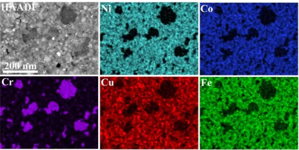
Figure 5. Representative HAADF-STEM image of CrFeCoNiCu alloy film annealed at 700 °C, and its EDS elemental maps showing the distribution of Cr, Fe, Co, Cu, and Ni in the film.
Besides that, the Cr map (Figure 5) shows that smaller grains, with diameter 20–50 nm could also be enriched in Cr. Fe, Co, and Ni were distributed rather evenly in the remaining matrix (Figure 5). The Cu distribution, however, proved to be inhomogeneous on 10–20 nm scale. The elemental maps also indicate that the Cr-rich grains were depleted in Fe, Co, Ni, and Cu, as the Cr map and maps of the other four metal components were complementary.
A general HRTEM view of the structure is shown in Figure 6a. In this figure the remaining mainly FCC HEA metallic phase was seen having a grain size of 20–50 nm, and larger grains (marked A in Figures 3a and 6a) of the Cr-rich phase were present.
The internal structure in the large grains displays a striped contrast, corresponding to a large lattice spacing in them. The HRTEM image of these crystallites (grains) and the fast Fourier transform (FFT) diffraction pattern in the insert is shown in Figure 6b. The lattice fringe image was dominated by two spacings making 86° with each other and having periods 0.59 nm and 0.204 nm, not possible in the BCC cell. However, the Fourier transform implies close structural relationship of the Cr-rich phase large grains with the BCC phase formed at 450 °C (aBCC = 0.294 ± 0.010 nm). The structural relationship was illustrated by the directions corresponding to the BCC lattice in Figure 6b. Doubling the periodicity with respect to BCC phase was evident in the Fourier transform; however, based on the appearance of the 1/(4 × 0.294) nm−1 periodicity in the reciprocal lattice, (2 × 2 × 4)aBCC size repeating units were deduced for the structure of this grain (Figure 6a). Additionally, a continuous/diffuse scattering of the ½½ l reflections was observed parallel to the [001]*BCC direction, indicating non-periodicity along the crystallographic c axis (Figure 6b). In Figure 6c,d Fourier filtered images of the same area are shown.
Figure 5.Representative HAADF-STEM image of CrFeCoNiCu alloy film annealed at 700◦C, and its EDS elemental maps showing the distribution of Cr, Fe, Co, Cu, and Ni in the film.
The chemical composition of different morphologies can be found in Table2. The small grained areas are close in composition to the original HEA with some deficit of Cr and surplus of Cu in them (locations M1 and M2 in Table2and Figure4). Locations A1 and A2 in Table2and Figure4correspond to dark gray grains and contain mainly Cr (about 63 at. %), while Ni and Co content was significantly less, as indicated by elemental maps in Figure5. These results show that separation of the components in the originally single phase, homogeneous solid solution HEA film took place during the annealing above 600◦C.
Besides that, the Cr map (Figure5) shows that smaller grains, with diameter 20–50 nm could also be enriched in Cr. Fe, Co, and Ni were distributed rather evenly in the remaining matrix (Figure5).
The Cu distribution, however, proved to be inhomogeneous on 10–20 nm scale. The elemental maps also indicate that the Cr-rich grains were depleted in Fe, Co, Ni, and Cu, as the Cr map and maps of the other four metal components were complementary.
A general HRTEM view of the structure is shown in Figure6a. In this figure the remaining mainly FCC HEA metallic phase was seen having a grain size of 20–50 nm, and larger grains (marked A in Figures3a and6a) of the Cr-rich phase were present.
Table 2.Chemical composition of the HEA film annealed at 700◦C in areas marked in Figure4and measured by energy dispersive X-ray spectroscopy (EDS) in STEM.
Z Element Family Area in Figure4
A1 A2 M1 M2
Atomic Fraction (%)
24 Cr K 62.39 63.29 15.06 10.27
26 Fe K 12.93 13.86 17.63 19.11
27 Co K 6.46 9.09 18.57 18.18
28 Ni K 4.10 1.28 19.28 24.22
29 Cu K 14.12 12.47 29.47 28.22
Coatings 2020, 10, x FOR PEER REVIEW 9 of 15
Figure 6. (a) Low magnification image showing spatial relationship of the Cr-rich intermetallic phase (A) and the residual HEA phase formed during in-situ annealing up to 700 °C. (b) Lattice resolution image of the Cr-rich phase. On the Fourier transform (lower right corner) two directions, corresponding to the unit cell of BCC phase (with a0 = 0.294 nm) are indicated. Note the diffuse scattering parallel to [001]*. Black arrows indicate 1.18 nm periodicity, which is four times the lattice parameter (0.294 nm) of the BCC lattice. (c) Enlarged Fourier filtered image made with the discrete (001 and 110 in BCC notation) Fourier components of (b), (d) Enlarged Fourier filtered image made with the ½½l diffuse scattering (continuous line) on (b). White arrows indicate non-periodic fringes parallel to (001). Note the presence of the 0.588 nm periodicity in (d) as well.
In Figure 6c the periodic components corresponding to the BCC 001 and 110 distances are shown and all the other components were removed from the image by filtering. The image visualizes the periods, corresponding to aBCC = 0.294 nm = d001 and at an angle of 90° to this, a period of spacing 0.208 nm ((110) planes in the BCC cell) representing the contribution of the BCC phase (Table 1) to the structure of these grains. Figure 6d, shows a Fourier filtered image made with the ½½l (BCC notation) diffuse scattering (continuous lines) in the insert of Figure 6b. The white arrows in the image indicate atomic planes parallel to 001 fringes seen in Figure 6c, however, at a rather random spacing (planar disorder). Nevertheless, the multiplies of the basic fringe spacing of the BCC lattice (d002 = 0.147 nm) in the [001] direction, i.e., the 0.294 nm and 0.588 nm (2 × aBCC) still can be observed.
Moreover, the [001] direction of the BCC lattice coincides with [001] of the (2 × 2 × 4) aBCC size cell. So, the Cr-rich grains named A type in Figure 6a (and A in all other figures) can be considered a Cr-rich intermetallic phase with a unit cell 2 × 2 × 4 times the unit cell of the BCC phase, observed at and above 450 °C.
In Figure 7 the HREM analysis of the type “voids” (B in Figure 3a) was carried out. As one can see, these areas were really voids in the metallic film, however, they contained material in the form of an apparently amorphous layer and small, 5–10 nm in size crystalline particles. The amorphous layer could be considered to be mainly the supporting SiOx layer. The analysis of the FFT diffraction pattern results in an FCC phase with about 0.42 nm lattice parameter (Figure 7c).
Figure 6.(a) Low magnification image showing spatial relationship of the Cr-rich intermetallic phase (A) and the residual HEA phase formed during in-situ annealing up to 700◦C. (b) Lattice resolution image of the Cr-rich phase. On the Fourier transform (lower right corner) two directions, corresponding to the unit cell of BCC phase (with a0=0.294 nm) are indicated. Note the diffuse scattering parallel to [001]*. Black arrows indicate 1.18 nm periodicity, which is four times the lattice parameter (0.294 nm) of the BCC lattice. (c) Enlarged Fourier filtered image made with the discrete (001 and 110 in BCC notation) Fourier components of (b), (d) Enlarged Fourier filtered image made with the1212ldiffuse scattering (continuous line) on (b). White arrows indicate non-periodic fringes parallel to (001). Note the presence of the 0.588 nm periodicity in (d) as well.
The internal structure in the large grains displays a striped contrast, corresponding to a large lattice spacing in them. The HRTEM image of these crystallites (grains) and the fast Fourier transform (FFT) diffraction pattern in the insert is shown in Figure6b. The lattice fringe image was dominated by two spacings making 86◦with each other and having periods 0.59 nm and 0.204 nm, not possible in the BCC cell. However, the Fourier transform implies close structural relationship of the Cr-rich phase large grains with the BCC phase formed at 450◦C (aBCC=0.294±0.010 nm). The structural relationship
Coatings2020,10, 60 9 of 15
was illustrated by the directions corresponding to the BCC lattice in Figure6b. Doubling the periodicity with respect to BCC phase was evident in the Fourier transform; however, based on the appearance of the 1/(4×0.294) nm−1periodicity in the reciprocal lattice, (2×2×4)aBCCsize repeating units were deduced for the structure of this grain (Figure6a). Additionally, a continuous/diffuse scattering of the
1 21
2lreflections was observed parallel to the [001]*BCCdirection, indicating non-periodicity along the crystallographiccaxis (Figure6b). In Figure6c,d Fourier filtered images of the same area are shown.
In Figure6c the periodic components corresponding to the BCC 001 and 110 distances are shown and all the other components were removed from the image by filtering. The image visualizes the periods, corresponding to aBCC=0.294 nm=d001and at an angle of 90◦to this, a period of spacing 0.208 nm ((110) planes in the BCC cell) representing the contribution of the BCC phase (Table1) to the structure of these grains. Figure6d, shows a Fourier filtered image made with the1212l(BCC notation) diffuse scattering (continuous lines) in the insert of Figure6b. The white arrows in the image indicate atomic planes parallel to 001 fringes seen in Figure6c, however, at a rather random spacing (planar disorder). Nevertheless, the multiplies of the basic fringe spacing of the BCC lattice (d002=0.147 nm) in the [001] direction, i.e., the 0.294 nm and 0.588 nm (2×aBCC) still can be observed. Moreover, the [001] direction of the BCC lattice coincides with [001] of the (2×2×4) aBCCsize cell. So, the Cr-rich grains named A type in Figure6a (and A in all other figures) can be considered a Cr-rich intermetallic phase with a unit cell 2×2×4 times the unit cell of the BCC phase, observed at and above 450◦C.
In Figure7the HREM analysis of the type “voids” (B in Figure3a) was carried out. As one can see, these areas were really voids in the metallic film, however, they contained material in the form of an apparently amorphous layer and small, 5–10 nm in size crystalline particles. The amorphous layer could be considered to be mainly the supporting SiOxlayer. The analysis of the FFT diffraction pattern results in an FCC phase with about 0.42 nm lattice parameter (FigureCoatings 2020, 10, x FOR PEER REVIEW 7c). 10 of 15
Figure 7. (a) Post-annealing high resolution image of the HEA (annealed at 700 °C) of an area marked B in Figure 3. White rectangle indicates the area of subsequent EDS mapping. (b) Magnified image of the area B in (a) showing crystalline particles. (c) Fast Fourier transform (FFT) diffraction of the region in (b) indexed according to an FCC oxide structure with lattice parameter a = 0.42 nm.
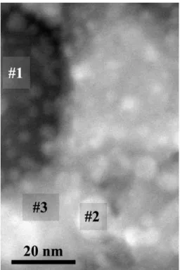
Local EDS measurement of the composition inside the “void” proves that these areas were dominated by Cr accompanied by only a little amount of the remaining HEA metal components (area
#1 in Figure 8 and in Table 3). Areas #2 and #3 in Figure 8 and in Table 3 indicate compositional fluctuation on the tens of nm scale implying that the redistribution of components is going on. The composition measured in the whole area in Figure 8 demonstrates that the composition of the original HEA phase on average was basically preserved in the film. These results lead to the conclusion that the crystals, which remained in the voids have a possible composition Cr4-xMxO4 (M can be Co, Fe, Ni or Cu) corresponding to four molecules in the FCC unit cell of either CrO [25] or a HEA-oxide [26]
type phase.
Table 3. Elemental composition measured in the areas marked in Figure 8. Analysis of spectrum: from a hole (Area#1), two small areas in the matrix (Areas #2 and #3) and the whole area of the STEM image in Figure 8.
Z Element Family Atomic Fraction (%)
Area #1 Area #2 Area #3 The Whole Area
24 Cr K 83.62 8.20 29.04 21.00
26 Fe K 1.86 22.09 21.96 21.37
27 Co K 1.56 18.84 19.61 19.95
28 Ni K 0.66 20.93 17.28 19.44
29 Cu K 12.29 29.94 12.10 18.24
Figure 7.(a) Post-annealing high resolution image of the HEA (annealed at 700◦C) of an area marked B in Figure3. White rectangle indicates the area of subsequent EDS mapping. (b) Magnified image of the area B in (a) showing crystalline particles. (c) Fast Fourier transform (FFT) diffraction of the region in (b) indexed according to an FCC oxide structure with lattice parameter a=0.42 nm.
Local EDS measurement of the composition inside the “void” proves that these areas were dominated by Cr accompanied by only a little amount of the remaining HEA metal components (area #1 in Figure8and in Table3). Areas #2 and #3 in Figure8and in Table3indicate compositional fluctuation on the tens of nm scale implying that the redistribution of components is going on. The composition measured in the whole area in Figure8demonstrates that the composition of the original HEA phase on average was basically preserved in the film. These results lead to the conclusion that the crystals, which remained in the voids have a possible composition Cr4-xMxO4(M can be Co, Fe, Ni or Cu) corresponding to four molecules in the FCC unit cell of either CrO [25] or a HEA-oxide [26] type phase.
Coatings 2020, 10, x FOR PEER REVIEW 11 of 15
Figure 8. STEM HAADF image of the film annealed at 700 °C and the areas used for quantitative EDS analysis.
4. Discussion
As we could clearly see from Figure 2, the changes of the structural transformations of the as- deposited CrFeCoNiCu HEA thin film could be divided into three temperature intervals. There were no changes below 400 °C, minor changes occur below 600 °C, and from this temperature rapid morphological transformations and separation of the components took place.
In the low temperature range below 400 °C at the present annealing periods no measurable changes occurred in the structure of the FCC CrFeCoNiCu HEA film.
During the annealing step at 450 °C a minor quantity of a new phase was observed with BCC lattice of a = 0.294 nm very close to that of Cr (a = 0.291 nm) and Fe (a = 0.288 nm). However, the identification of the grains of the BCC phase proved not to be straightforward. The BCC grains were located among the grains of the host FCC phase, having the same grain size. (Figure 2). This situation was preserved up to 550 °C. However, the nature of the FCC to BCC phase transformation was unclear. It could occur by nucleation and growth, probably accompanied by separation of components or by massive transformation without it. It could also happen by martensitic transformation, which according to [27], could occur by a simple deformation mechanism, leading to well defined crystallographic relationship of the starting FCC and the resulting BCC phases. In the case of the two diffusionless transformation mechanisms, i.e., massive and martensitic, the original random distribution of the components was preserved. In the case of diffusion, transformation implies chemical ordering of components (without their separation) in the originally single phase FCC HEA structure, containing the five constituting components in random distribution. Chemical ordering induces the formation of superstructures, which manifests itself in the appearance of extra reflections in the diffraction pattern with respect to the random FCC or BCC phases. As there were no extra (forbidden) reflections detected with respect to the HEA FCC and the BCC (consequently HEA BCC) phases up to 550 °C (Figure 2a) the preservation of the fully random distribution of the components was confirmed. This, together with the unchanged morphology supports that below 550
°C the kinetics of formation of the HEA BCC phase should take place by a diffusionless mechanism.
Similar diffusionless transformation was reported for AlxCoFeNiCrCu bulk alloys [10] and attributed to the changing of Al content. In the present case the transformation in the CrFeCoNiCu HEA film occurred without any BCC forming additives and was triggered only by the increasing temperature.
Figure 8. STEM HAADF image of the film annealed at 700◦C and the areas used for quantitative EDS analysis.
Table 3. Elemental composition measured in the areas marked in Figure8. Analysis of spectrum:
from a hole (Area#1), two small areas in the matrix (Areas #2 and #3) and the whole area of the STEM image in Figure8.
Z Element Family Atomic Fraction (%)
Area #1 Area #2 Area #3 The Whole Area
24 Cr K 83.62 8.20 29.04 21.00
26 Fe K 1.86 22.09 21.96 21.37
27 Co K 1.56 18.84 19.61 19.95
28 Ni K 0.66 20.93 17.28 19.44
29 Cu K 12.29 29.94 12.10 18.24
4. Discussion
As we could clearly see from Figure2, the changes of the structural transformations of the as-deposited CrFeCoNiCu HEA thin film could be divided into three temperature intervals. There were no changes below 400◦C, minor changes occur below 600◦C, and from this temperature rapid morphological transformations and separation of the components took place.
In the low temperature range below 400◦C at the present annealing periods no measurable changes occurred in the structure of the FCC CrFeCoNiCu HEA film.
Coatings2020,10, 60 11 of 15
During the annealing step at 450◦C a minor quantity of a new phase was observed with BCC lattice of a=0.294 nm very close to that of Cr (a=0.291 nm) and Fe (a=0.288 nm). However, the identification of the grains of the BCC phase proved not to be straightforward. The BCC grains were located among the grains of the host FCC phase, having the same grain size. (Figure2). This situation was preserved up to 550◦C. However, the nature of the FCC to BCC phase transformation was unclear. It could occur by nucleation and growth, probably accompanied by separation of components or by massive transformation without it. It could also happen by martensitic transformation, which according to [27], could occur by a simple deformation mechanism, leading to well defined crystallographic relationship of the starting FCC and the resulting BCC phases. In the case of the two diffusionless transformation mechanisms, i.e., massive and martensitic, the original random distribution of the components was preserved. In the case of diffusion, transformation implies chemical ordering of components (without their separation) in the originally single phase FCC HEA structure, containing the five constituting components in random distribution. Chemical ordering induces the formation of superstructures, which manifests itself in the appearance of extra reflections in the diffraction pattern with respect to the random FCC or BCC phases. As there were no extra (forbidden) reflections detected with respect to the HEA FCC and the BCC (consequently HEA BCC) phases up to 550◦C (Figure2a) the preservation of the fully random distribution of the components was confirmed. This, together with the unchanged morphology supports that below 550◦C the kinetics of formation of the HEA BCC phase should take place by a diffusionless mechanism. Similar diffusionless transformation was reported for AlxCoFeNiCrCu bulk alloys [10] and attributed to the changing of Al content. In the present case the transformation in the CrFeCoNiCu HEA film occurred without any BCC forming additives and was triggered only by the increasing temperature. Summarizing, it can be inferred that the diffusionless formation mechanism of the HEA BCC phase is the first stage of transformations in the CrFeCoNiCu alloy films before the separation processes of components start and formation of further phases occurs.
Above 600◦C, (Figures2and3), we could establish that besides the residual matrix, in which the FCC HEA grains represent the majority phase, other grains an order of magnitude larger in size exist.
These larger grains, which mostly contain chromium, and indicate that separation of components occurred (Figure4and Table2as well as Figure5), have superstructure reflections and also diffuse scattering in their FFT diffraction pattern. The superstructure reflections implying large unit cell parameters are integer multiples of the cell parameter of the HEA BCC phase. An example of such a Cr-rich grain with 2×2×4aBCCcell size is presented in Figure6. We attributed the formation of the large (2×2×4 times the BCC) unit cell Cr-rich phase to the ordering processes during the ongoing separation of components in the HEA alloy.
As indicated by the diffuse scattering (Figure 6b) observed in the Fourier transforms of the Cr-rich grains, these grains exhibit an aperiodic structure as well, which is related to chemical disorder.
The direction of diffuse scattering coincides with the [001]* reciprocal vector of the BCC phase and can be attributed to planar disorder in these crystals. The proposed planar disorder means, that the atomic planes of the large unit cell of the Cr-rich phase normal to the [001] direction do not have a real translational symmetry along [001] (Figure6d) in the entire grain, but one or more of the five components concentrates on different (008) planes of the Cr-rich grain. However, other ordering patterns are also possible. This means, that the structure is regular for not more than a few unit cells (Figure6d), then the ordering pattern changes. In some cases this can mean single atomic planes with different order/composition from their neighborhood resulting in “infinite” reciprocal rods, parallel to the [001]* reciprocal vectors as observed in Figure6b in the form of the streaks. However, as individual reflections in the FFT diffraction pattern along [001]* containing the BCC reciprocal vectors remain visible, we suppose, that this kind of planar disorder is the property of the large cell, within which the composing former BCC cells (a=0.294 nm) are preserved at least partly (Figure6c). This explains the decrease of the number of BCC type reflections at temperatures above 650◦C as seen in Figures2a and 3, because the reflections of the Cr-rich phase and the BCC phase coincide only partly. It also has to be noted that, according to our HRTEM observations, various pathways of separation and ordering
may exist, the example presented is only one of them. This can account for the numerous scattered reflections in the diffraction pattern taken at 700◦C (Figure3) practically without regular positioning, which hampers a general description of these structures. A possible phase, present in the annealed up to 700◦C films, is the sigma phase [28,29]. It is known that Cr is a strong sigma phase former below 700◦C, which can be deduced from the binary alloy phase diagrams of Cr-Co, Cr-Fe, or from Cr-Co-Fe ternary phase diagram [30]. The crystal structure of the sigma phase [29] belongs to the tetragonal space group with lattice parameters of a=8.8 Å and c=4.5 Å.
It was reported in the literature [10,21,22,31] that the nucleation pathway of Cr containing sigma phase prototype of Cr-Co and Cr-Fe alloys formed either through the BCC/B2 phase or directly from the FCC matrix. BCC/B2 phase prototypes can be transformed to sigma phase due to the high affinity of Cr toward Co, Cr, or Fe. In our case we believe that Cr–rich phase is developed from the HEA BCC phase observed in the 450–650◦C temperature interval and serves as a precursor of the sigma phase. This is supported also by the fact that the HEA BCC phase and the Cr-rich phase have a strict epitaxial relation.
From Table1we can see, that after the annealing at 700◦C the structure is probably composed of several phases not easily separable from each other due to the observed crystallographic similarities.
The textured fraction of the FCC HEA phase is still the dominating one with a fraction of it transformed to the L12 phase. Having a closer look to the nature of the 0.248 nm ring (Figure3) we could conclude that it has a mixed character. It has discrete diffraction spots, with a preferred orientation coinciding with that of the FCC HEA phase, which can be attributed to an ordered L12 phase. On the other hand, the 0.248 nm ring has a faint continuous ring as well, indicating a much smaller crystallite size.
This ring we attributed to the FCC oxide phase, being a surface Cr-oxide with a=0.42 nm as proven by HRTEM (Figure8, Table3). The most difficult task was the identification of the HEA BCC and the ordered Cr-rich phases in the diffraction pattern (Figure3). HEA BCC rings completely overlapped with those of the L12 phase. Regarding the Cr-rich grains, the large periodicities corresponding to the 2×2×4aBCCand similar unit cells were not detected in the in-situ SAED pattern (Figure2a), maybe due to their low intensities (see also Figure3). All the other reflections coincided with the FCC and L12 HEA phases, and could not be separated even on the basis of the continuous or spotty nature of the diffraction rings (Table1). However, they were present in the FFT patterns of the high resolution images (Figure6). Furthermore, post annealing elemental mapping of the samples (Figure5) shows that small grains rich in either Cr or Cu are present in the structure indicating that the separation of components begins with Cr and Cu. So, the conclusion was that short time (5 min) 50◦C annealing steps result in a multiphase structure representing the initial stages of transformations, which were still far from equilibrium.
Summarizing the events above 600◦C, the HEA BCC grains served as precursors of the newly forming large Cr-rich grains and a transformation through ordering processes led to larger lattice periods in this phase. The grains of the Cr-rich phase were growing mainly laterally, remaining in the plane of the film (Figure5and areas 1 and 3 in Table3). They were growing fast at the expense of the surrounding (still mainly nanocrystalline FCC HEA) matrix. During their growth, as it was related to the separation of the components from the surrounding matrix, the rate limiting kinetics must be volume diffusion. To get some insight into the kinetics of this process the activation energy of the growth rate of Cr-rich grains was estimated according to the procedure used in [32]. The calculated value of the activation energy for this process is 160±30 kJ/mole and corresponded fairly well to that of bulk diffusion of Fe in Cu 187 kJ/mol in the temperature range between 650 and 1000◦C [33]. On this basis the rate limiting process in the high temperature range (T≥600◦C) could be attributed to the lattice self-diffusion of components in the HEA alloy.
Coatings2020,10, 60 13 of 15
The strong affinity of Cr to oxygen resulting in a surface layer of Cr3MO4(M can be: Fe, Co, Ni, or Cu) like composition in the void regions as well as over the whole film area (Figures7and8) could be possibly responsible for an anticorrosive property of these alloys.
5. Conclusions
The CrFeCoNiCu HEA alloy films were stable in their FCC structure up to 400◦C.
At 450◦C a HEA BCC phase appeared in the film. This change was considered to occur by a diffusionless phase transformation. The structure, composition and grain size of the newly formed BCC grains corresponded to the HEA FCC grains.
The separation of the components began above 550◦C. The actual activation energy of this process was estimated to be around 160 kJ/mol. It must be related to lattice diffusion in the HEA alloy, which should be the rate limiting process during transformations above 550◦C. These transformations were:
• A new phase with a large unit cell, epitaxial to the already formed BCC phase started growing.
The cell parameters correspond to 2×2×4 units of the BCC cell. The crystals possessed a planar disorder of atomic planes in one of the<001>directions, though the BCC lattice was preserved as an internal skeleton of their structure.
• Formation of voids occurred in the metallic part of the film. These voids were, however, still containing a nano-crystalline phase of the composition close to CrO and having an FCC lattice of about 0.42 nm period. This must be the part of a surface chromium oxide layer, possibly contributing to corrosion resistance of these films.
Author Contributions:G.R. designed the project. M.A. and G.R. carried out the deposition and the in-situ TEM heating experiments. Post annealing analyses (HRTEM, elemental mapping) were done by V.K.K. All authors discussed the results and approved the final manuscript. All authors have read and agreed to the published version of the manuscript.
Funding: This study was funded by the Hungarian National Research, Development and Innovation Office through the OTKA NN112156 project.
Acknowledgments: The authors also acknowledge the VEKOP-2.3.3-15-2016-00002 project of the European Structural and Investment Funds. V.K.K. is indebted to the János Bolyai Fellowship of the Hungarian Academy of Sciences and theÚNKP-19-4 New National Excellence Program of the Ministry for Innovation and Technology.
Conflicts of Interest:The authors declare no conflict of interest.
References
1. Cantor, B.; Chang, I.T.H.; Knight, P.; Vincent, A.J.B. Microstructural development in equiatomic multicomponent alloys.Mater. Sci. Eng. A2004,375, 213–218. [CrossRef]
2. Zhang, Y.; Zuo, T.T.; Tang, Z.; Gao, M.; Dahmen, K.A.; Liaw, P.K.; Lu, Z.P. Microstructures and properties of high entropy alloys.Prog. Mater. Sci.2014,61, 1–93. [CrossRef]
3. Gao, M.C. Progress in High-Entropy Alloys.JOM2013,65, 1749–1750. [CrossRef]
4. Lu, Y.P.; Gao, X.Z.; Jiang, L.; Chen, Z.N.; Wang, T.; Jie, J.C.; Li, T.J. Directly cast bulk eutectic and near-eutectic high entropy alloys with balanced strength and ductility in a wide temperature range.Acta Mater.2017,124, 143. [CrossRef]
5. Kao, Y.F.; Chen, T.J.; Chen, S.K.; Yeh, J.W. Microstructure and mechanical property of as-cast,-homogenized, and-deformed AlxCoCrFeNi (0≤x≤2) high-entropy alloys.J. Alloy. Compd.2009,488, 57. [CrossRef]
6. Miracle, D.B.; Senkov, O.N. A critical review of high entropy alloys and related concepts.Acta Mater.2017, 122, 448–511. [CrossRef]
7. Xu, X.D.; Liu, P.; Guo, S.; Hirata, A.; Fujita, T.; Nieh, T.G.; Liub, C.T.; Chena, M.W. Nanoscale phase separation in a fcc-based CoCrCuFeNiAl0.5 high-entropy alloy.Acta Mater.2015,84, 145–152. [CrossRef]
8. Shun, T.T.; Hung, C.H.; Lee, C.F. Formation of ordered/disordered nanoparticles in FCC high entropy alloys.
J. Alloy. Compd.2010,493, 105–109. [CrossRef]
9. Wang, J.; Niu, S.; Guo, T.; Kou, H.; Li, L. The FCC to BCC phase transformation kinetics in an Al0.5CoCrFeNi high entropy alloy.J. Alloy. Compd.2017,710, 144–150. [CrossRef]
10. Wang, W.R.; Wang, W.L.; Wang, S.C.; Tsai, Y.C.; Lai, C.H.; Yeh, J.W. Effects of Al addition on the microstructure and mechanical property of AlxCoCrFeNi high-entropy alloys.Intermetallics2012,26, 44–51. [CrossRef]
11. Pickering, E.J.; Muñoz-Moreno, R.; Stone, H.J.; Jones, N.J. Precipitation in the equiatomic high-entropy alloy CrMnFeCoNi.Scr. Mater.2016,113, 106–109. [CrossRef]
12. Otto, F.; Dlouhý, A.; Pradeep, K.G.; Kubenov, M.; Raabe, D.; Eggeler, G.; George, E.P. Decomposition of the single-phase high-entropy alloy CrMnFeCoNi after prolonged anneals at intermediate temperatures.
Acta Mater.2016,112, 40–52. [CrossRef]
13. He, F.; Wang, Z.; Wu, Q.; Li, J.; Wang, J.; Liu, C.T. Phase separation of metastable CoCrFeNi high entropy alloy at intermediate temperatures.Scr. Mater.2017,126, 15–19. [CrossRef]
14. Zhang, Y.; Zhou, Y.J.; Lin, J.P.; Chen, G.L.; Liaw, P.K. Solid Solution Phase Formation Rules for Multi-Component Alloys.Adv. Eng. Mater.2008,10, 534–538. [CrossRef]
15. An, Z.; Jia, H.; Wu, Y.; Rack, P.D.; Patchen, A.D.; Liu, Y.; Ren, Y.; Li, N.; Liaw, P.K. Solid-solution CrCoCuFeNi high-entropy alloy thin films synthesized by sputter deposition.Mater. Res. Lett.2015,3, 203–209. [CrossRef]
16. Zhang, L.J.; Fan, J.T.; Liu, D.J.; Zhang, M.D.; Yu, P.F.; Jing, Q.; Ma, M.Z.; Liaw, P.K.; Li, G.; Liu, R.P.
The microstructural evolution and hardness of the equiatomic CoCrCuFeNi high-entropy alloy in the semi-solid state.J. Alloy. Compd.2018,745, 75–83. [CrossRef]
17. Park, N.; Watanabe, I.; Terada, D.; Yokohama, Y.; Liaw, P.K.; Tsuji, N. Recrystallization Behavior of CoCrCuFeNi high-entropy alloy.Metall. Mater. Trans. A2015,46, 1481–1487. [CrossRef]
18. Oh, S.M.; Hong, S.I. Microstructural stability and mechanical properties of equiatomicCoCrCuFeNi, CrCuFeMnNi, CoCrCuFeMn alloys.Mater. Chem. Phys.2018,210, 120–125. [CrossRef]
19. Chen, T.K.; Shun, T.T.; Yeh, J.W.; Wong, M.S. Nanostructured nitride films of multi-element high-entropy alloys by reactive DC sputtering.Surf. Coat. Technol.2004,188, 193–200. [CrossRef]
20. Braeckman, B.R.; Misják, F.; Radnóczi, G.; Depla, D. The influence of Ge and in addition on the phase formation of CoCrCuFeNi high-entropy alloy thin films.Thin Solid Film.2016,616, 703–710. [CrossRef]
21. Dolique, V.; Thomann, A.L.; Brault, P.; Tessier, Y.; Gillon, P. Thermal stability of AlCoCrCuFeNi high entropy alloy thin films studied by in-situ XRD analysis.Surf. Coat. Technol.2010,204, 1989–1992. [CrossRef]
22. Rao, J.C.; Diao, H.Y.; Ocelík, V.; Vainchtein, D.; Zhang, C.; Kuo, C.; Tang, Z.; Guo, W.; Poplawsky, J.D.;
Zhou, Y.; et al. Secondary phases in AlxCoCrFeNi high-entropy alloys: An in-situ TEM heating study and thermodynamic appraisal.Acta Mater.2017,131, 206–220. [CrossRef]
23. Nagase, T.; Rack, P.D.; Noh, J.H.; Egami, T. In-situ TEM observation of structural changes in nano-crystalline CoCrCuFeNi multicomponent high-entropy alloy (HEA) under fast electron irradiation by high voltage electron microscopy (HVEM).Intermetallics2015,59, 32–42. [CrossRef]
24. Zhang, Y.W.; Tunes, M.A.; Crespillo, M.L.; Zhang, F.X.; Boldman, W.L.; Rack, P.D.; Jiang, L.; Xu, C.; Greaves, G.;
Donnelly, S.E.; et al. Thermal stability and irradiation response of nanocrystalline CoCrCuFeNi high-entropy alloy.Nanotechnology2019,30, 15. [CrossRef]
25. Lux, H.; Illmann, G. ZurKenntnis der Chrom (II) Salze und des Chrom (II) oxyds, II.Chem. Ber.1959,92, 9.
[CrossRef]
26. Dedoncker, R.; Radnóczi, G.; Abadias, G.; Depla, D. Reactive sputter deposition of CoCrCuFeNi in oxygen/argon mixtures.Surf. Coat. Technol.2019,378, 124–362. [CrossRef]
27. Sandoval, L.; Urbassek, H.M.; Entel, P. The Bain versus Nishiyama–Wassermann path in the martensitic transformation of Fe.New J. Phys.2009,11, 103027. [CrossRef]
28. Jette, E.R.; Foote, F. The Fe-Cr alloy system.Met. Alloy.1936,7, 207.
29. Bergman, B.G.; Shoemaker, D.P. The space group of sigma-FeCr crystal structure.J. Chem.Phys.1951,19, 515.
[CrossRef]
30. Okamoto, H.; Schlesinger, M.E.; Mueller, E.M.Alloy Phase Diagram; ASM International: Materials Park, OH, USA, 1992.
31. Shivam, V.; Basu, J.; Pandey, V.K.; Shadangi, Y.; Mukhopadhyay, N.K. Alloying behaviour, thermal stability and phase evolution in quinary AlCoCrFeNi high entropy alloy.Adv. Powder Technol.2018,29, 2221–2230.
[CrossRef]
Coatings2020,10, 60 15 of 15
32. Nagy, K.H.; Misják, F. In-situ transmission electron microscopy study of thermal stability and carbide formation in amorphous Cu-Mn/C films for interconnect applications. J. Phys. Chem. Solids2018, 121, 312–318. [CrossRef]
33. Prokoshkina, D.; Rodin, A.; Esin, V. About Fe Diffusion in Cu. Defect Diffus. Forum2012,323, 171–176.
[CrossRef]
©2020 by the authors. Licensee MDPI, Basel, Switzerland. This article is an open access article distributed under the terms and conditions of the Creative Commons Attribution (CC BY) license (http://creativecommons.org/licenses/by/4.0/).