Digital Technics
Lovassy, Rita
A projekt az Új Széchenyi terv keretében a TÁMOP-4.1.2.A/1-11/1-2011-0041 „Audio-vizuális v-learning és e-learning tananyag- és képzésfejlesztés az Óbudai
Egyetem Kandó Kálmán Villamosmérnöki Karán” támogatásával valósult meg.
Preface ... ix
1. Fundamental Principles of Digital Logic ... 1
1. Boolean Algebra and its Relation to Digital Circuits ... 2
1.1. Logic Variables ... 3
1.2. Basic Boolean Operations ... 3
1.3. Boolean Theorems ... 5
1.4. De Morgan’s Laws ... 6
2. Truth Table and Basic Boolean Functions ... 6
2.1. One Variable Boolean Functions ... 7
2.2. Two Variable Boolean Functions ... 7
3. Boolean Expressions ... 8
3.1. Obtaining a Boolean expression from a truth table ... 8
3.2. Sum-of-Products (SOP) Form, the Minterm Canonical Form ... 9
3.3. Minterm ... 9
3.4. Product-of-Sums (POS) Form, Maxterm Canonical Form ... 10
3.5. Maxterm ... 10
3.6. Minterm to Maxterm Conversion ... 10
4. Minimization of Logic Functions ... 11
4.1. Algebraic minimization using Boolean theorems ... 11
4.2. Graphic minimization, Karnaugh map (K-map) ... 12
4.3. Minimal Sums ... 12
4.4. Two Variable Karnaugh Maps ... 13
4.5. Three - Variable Karnaugh Maps ... 14
4.6. Four-Variable Karnaugh Maps ... 17
4.7. Karnaugh Map for Minimalization of a Four Variables Logic Function Expressed in Product-Of-Sums ... 20
4.8. Incompletely Specified Logic Function ... 22
5. Combinational Logic Networks ... 22
5.1. Logic Gates ... 23
5.2. The EXCLUSIVE OR and NOT EXCLUSIVE OR Functions ... 26
5.3. Standard Forms for Logic Functions, Synthesis Using Standard Expressions and the Corresponding Circuits with NAND or NOR Gates ... 27
5.4. Problems ... 29
2. Number Systems ... 31
1. Positional Number Systems ... 31
1.1. Decimal Number System ... 31
1.2. Binary Number System ... 31
1.3. Conversion from binary to decimal ... 31
1.4. Conversion from decimal to binary ... 32
1.5. Octal and Hexadecimal Numbers ... 33
1.6. Conversion from octal or hexadecimal to decimal ... 33
1.7. Conversion from octal and hexadecimal to binary ... 34
2. Binary Arithmetic ... 34
2.1. Binary Addition ... 34
2.2. Binary Subtraction ... 36
2.3. Binary Multiplication ... 37
2.4. Binary Division ... 38
3. Signed Binary Numbers ... 38
3.1. Sign-Magnitude Representation ... 38
3.2. 1’s-Complement Representation ... 39
3.3. 2’s-Complement Representation ... 39
3.4. Addition with 2’s Complement Representation ... 40
4. Binary Codes and Decimal Arithmetic ... 40
4.1. Decimal Addition Using 8421 BCD Code ... 41
4.2. 7-Segment Code ... 42
4.3. Gray Code ... 44
4.4. Error Detection ... 44
4.5. Alphanumeric Codes ... 45
5. Functional Blocks ... 45
5.1. Code Converter ... 45
5.2. Binary Decoders ... 46
5.3. 2-to-4 Decoder ... 46
5.4. Binary Encoders ... 49
5.5. 4-to-2 Encoder ... 50
5.6. Priority Encoders ... 51
5.7. Multiplexer (MUX) ... 52
5.8. N-bit M x l Multiplexer ... 53
5.9. Demultiplexer ... 54
5.10. Comparators ... 55
5.11. Equality (Identity) Comparator ... 55
5.12. Magnitude Comparator- Carry-Ripple Style ... 56
5.13. Problems ... 57
3. Logic Circuits and Components ... 59
1. Digital Electronic Circuits ... 59
1.1. Transistor-Transistor Logic (TTL) ... 59
1.2. Inverter (NOT Gate) ... 59
1.3. TTL NAND gate ... 60
1.4. CMOS Logic ... 61
1.5. Basic CMOS Gates ... 61
1.6. Comparison of Logic Families ... 62
2. Sequential Logic Networks ... 63
3. Flip-Flops ... 64
3.1. The SR Latch and Flip-Flop ... 64
3.2. Clocked Latch and Flip-Flop ... 68
4.5. Synchronous Counters ... 76
4.6. Ring Counter ... 76
4.7. Johnson Counter ... 77
4.8. Case Study 1: Synchronous Modulo-3 Counter ... 77
4.9. Case Study 2: Design the 3-bit Gray code counter using JK flip-flops ... 78
4.10. Problems ... 81
4. Semiconductor Memories and Their Properties ... 83
1. Volatile Memories works ... 83
1.1. Static Random Access Memory (SRAM) ... 84
1.2. Dynamic Random Access Memory (DRAM) ... 85
1.3. Content-Addressable Memory (CAM) for Cache Memories ... 86
2. Nonvolatile Memories ... 86
2.1. Mask-Programmed ROM ... 87
2.2. Fuse-Based Programmable ROM - PROM ... 87
2.3. Erasable PROM - EPROM ... 88
2.4. EEPROM and Flash Memory ... 88
3. Memory Expansion ... 89
3.1. Example 1 Expand the address line ... 89
3.2. Example2 Expand the data line ... 91
3.3. Example 3 Expand the address and data line ... 91
3.4. Problems ... 91
5. Microprocessors Basics ... 92
1. Basic Microcomputer Organization ... 92
1.1. The Memory Unit ... 93
1.2. The Input/Output Units ... 93
2. General Purpose Microprocessor ... 93
2.1. Basic Datapath ... 94
2.2. Basic Control Unit ... 94
3. Instruction Sets ... 95
1.1. Analog signal ... 1
1.2. Digital signal ... 2
1.3. Electrical implementation of the AND and OR operations ... 4
1.4. Karnaugh maps: a) two-variable map; b) correspondence with truth table; c)example ... 13
1.5. Karnaugh map; F=B ... 14
1.6. Three-variable Karnaugh maps ... 15
1.7. Karnaugh map for Example 1.1 a ... 16
1.8. Karnaugh map for Example 1.1 b ... 16
1.9. Grouping on three-variable Karnaugh maps ... 17
1.10. Four-variable Karnaugh maps ... 18
1.11. Karnaugh map for Example 1.2 ... 19
1.12. Karnaugh map for Example 1.3 ... 20
1.13. Karnaugh map for Example 1.4 ... 21
1.14. Karnaugh map with don’t care conditions ... 22
1.15. Combinational logic network ... 23
1.16. Main gate symbols ... 25
1.17. AND gate with 8 inputs ... 26
1.18. Example for distinctive and rectangular shape logic symbols ... 27
1.19. a) AND-OR circuit; b) corresponding circuit with NAND only ... 28
1.20. a) OR-AND circuit; b) corresponding circuit with NOR only ... 29
2.1. Half adder logic diagram ... 35
2.2. Full adder logic diagram ... 36
2.3. 7-segment display ... 43
2.4. Code conversions ... 45
2.5. Binary decoder as a black box ... 46
2.6. 2-to-4 line decoder without Enable; a) truth table, b) gate level logic diagram ... 47
2.7. 2-to-4 line decoder with Enable a) truth table; b) gate level logic diagram ... 48
2.8. 3-to-8 decoder from 2-to-4 decoders ... 49
2.9. Binary encoder as a black box ... 50
2.10. 4-to-2 line encoder without Enable truth table and gate level logic diagram ... 51
2.11. Priory encoder truth table and logic circuit ... 52
2.12. 2-to-1 multiplexer ... 53
2.13. 4-bit 2 x 1 MUX a) internal design; b) block diagram ... 54
2.14. 4-bit equality comparator internal design, and its block symbol ... 55
2.15. 4-bit magnitude comparator a) internal design; b) block symbol ... 56
3.1. The transistor inverter and the input-output characteristics ... 60
3.9. and S R latch design using logic gates ... 67
3.10. Clocked SR Latch ... 68
3.11. Standard symbols for JK, D and T flip-flops ... 69
3.12. JK, D and T flip-flops Karnaugh maps ... 70
3.13. JK, D and T flip-flops excitation table and state diagram ... 71
3.14. Examples of standard graphics symbols ... 72
3.15. An SR master-slave flip-flop ... 73
3.16. 4-bit shift register a) logic diagram; b) waveforms ... 74
3.17. Mod-8 ripple counter ... 75
3.18. Divide-by-4 counter ... 76
3.19. Ring counter ... 76
3.20. Mod-3 counter a) circuit; b) waveform ... 78
3.21. State diagram and next state table for a 3-bit Gray code counter ... 79
3.22. Karnaugh maps and the next-state J and K outputs expressions ... 80
3.23. The hardware diagram of the 3-bit Gray code counter ... 81
4.1. RAM black box ... 83
4.2. Logical internal structure of a RAM ... 84
4.3. SRAM cell ... 85
4.4. DRAM cell ... 85
4.5. Simplified view of a conventional DRAM chip ... 86
4.6. 1024 x 32 ROM black box ... 87
4.7. Mask programmed ROM cells ... 87
4.8. Fuse-based ROM cells ... 87
4.9. EPROM cells ... 88
4.10. 1024 x 32 EEPROM black box ... 89
4.11. 256K x 8 memory from 64K x 8 chips and address ranges ... 90
4.12. 64K x 16 RAM, created from two 64K x 8 chips ... 91
5.1. Basic microcomputer organization ... 92
5.2. Basic architecture of a general purpose processor ... 94
1.4. Truth table - one variable Boolean functions ... 7 1.5. Truth table - two variables Boolean functions ... 7 1.6. Truth table for the Boolean expression ... 9
Preface
Digital circuits address the growing need for computer networking communications in the technological world today. Starting from the development of the integrated circuit in 1959 there has been a continuous interest in the understanding of new digital devices capable of performing complex functions.
It is the intent of this book to give an overview of the basic concepts and applications of digital technics, from Boolean algebra to microprocessors. The book highlights the distinction between combinational circuits and sequential circuits, deals with numeral systems, and gives a clear overview of main digital circuits, starting from gates through latches and flip-flops.
In the case of combinational circuits, further distinction between logic circuits and arithmetic circuits is provided. Furthermore, in the last two chapters, the book develops, in detail, the main memory structures, gives a basic microcomputer organization, and introduces a typical 8-bit microprocessor.
The material in this book is suitable for one or two semesters’ course of the bachelors’ degree program in electrical engineering or is also well-fitted for self study. The aim is to acquaint the future engineers with the fundamentals of digital technics, digital circuits, and with their characteristics and applications.
The book includes, as additional features, comprehensive examples and figures. At the end of each chapter a series of problems are given, which intend to give a broader view of the applicability of the concepts.
This book could be readily used in a completely new approach, as follows:
1. Number systems (Chapter “Number Systems”)
2. Combinational logic networks (subsection “Combinational Logic Networks”) with various Boolean logic gates followed by switches and implementation of Boolean logic gates using transistors (subsection “Digital Electronic Circuits“. Then the topics related to Boolean algebra and combinational logic optimization, minimization (subsections “Boolean Algebra and its Relation to Digital Circuits”− “Minimization of Logic Functions”)
3. Sequential logic networks (subsection “Sequential Logic Networks”) with synchronous and asynchronous circuits
4. Microprocessor basics (Chapter “Microprocessors Basics”) including memory structures (Chapter “Semiconductor Memories and Their Properties”)
1. fejezet - Fundamental Principles of Digital Logic
In general a signal can be defined as a value or a change in the value of a physical quantity. The signal represents, transmits or stores the information. The two main types of signal encountered in practice are analog and digital.
The analog signal is a continuous [http://en.wikipedia.org/wiki/Continuous_function] signal [http://en.wikipedia.org/wiki/Signal_%28circuit_theory%29], which represents the information directly with its value. The time evolution of the analog signal can be represented by a continuous function. It changes continuously in time and it can cover fully a given range, see Figure 1.1. In practice the analog signal usually refers to electrical signals [http://en.wikipedia.org/wiki/Electrical_signal]: especially voltage [http://en.wikipedia.org/wiki/Voltage], but current [http://
en.wikipedia.org/wiki/Electric_current], field strength, frequency [http://en.wikipedia.org/wiki/Frequency] etc. of the signal may also represent information.
For example, in sound recording, the voice (acoustic vibrations) is transformed by microphone (electro-acoustic transducer) into an electrical signal (voltage). Its characteristics are frequency range, signal-to-noise ratio, distortion, etc.
Analog circuits are designed for handling and processing analog signals and their input and output quantities are continuous. The advantages of such circuits are their ability to define infinite amounts of data, and they also use less bandwidth.
1.1. ábra - Analog signal
The digital signal represents the information divided into elementary parts in a numeric form using appropriate encoding. Sampling is performed at given times, and the numbers are attached to it. The digital signal therefore represents coded information, see Figure 1. 2.
1.2. ábra - Digital signal
Digital systems manage discrete quantities of information; they are suitable for handling and processing digital signals. For example, a digital circuit is able to manipulate speech and music which are continuous (non-discrete) quantities of information. The signal is sampled at 8000 samples per second. Each sample is quantized and coded by a single byte. After these steps we have discrete quantity of information:
•The cost is 64 Kbit/s which is too much.
•Digital Signal Processing techniques allow us to bring this amount down to as low as 2.4 Kbit/s [1].
Digital systems are less expensive, with reliable operation, are easy to manipulate, are flexible, are immune to noise to a certain extent, etc.
Some disadvantages of digital circuits are the sampling of errors; digital communications require greater bandwidth than analog to transmit the same information.
Different data converters are the interfaces between analog devices and digital systems. In many applications it is need to convert an analog signal in a digital form suitable for processing by a digital system. An analog-to-digital converter (A/D) measures the analog signal at a certain rate and turns each sample into some bit values. The digital-to-analog (D/A) converters produce an analog output from a given digital input.
The next chapter introduces the basic principles of digital logic, and deals with the study of digital systems. The digital computer is the best known of such systems. Within a digital system the elementary units operate like switches, being either ON or OFF. The logic circuits can be built up from any basic unit that has two different states, one for the 1 input/output, and one for the 0 input/output. The complicated logic functions are the interconnection of a large number of switches called logic gates. The formal mathematical tool which can be used to describe the behaviour of logic networks is called Boolean algebra. In this chapter various types of Boolean algebra expressions will be introduced, and the description of logic connection and their implementation with various logic gates will be discussed.
1. Boolean Algebra and its Relation to Digital Circuits
The operation of almost all modern digital computers is based on two-valued or binary systems. Propositions may be TRUE or FALSE, and are stated as functions of other propositions which are connected by the three basic logical connectives: AND, OR, and NOT. [2].
Boolean algebra was introduced in 1854 by George Boole [http://en.wikipedia.org/wiki/George_Boole] in his book: An Investigation of the Laws of Thought [3]. The connection between Boolean algebra and switching circuits was established by Claude Shannon [4]. He introduced the so called switching algebra as a main analytical tool to analyze and design logic circuits and networks. Typically, the units are in the form of switches that can be either ON or OFF (mapping to transistor-switches; high voltage means logic 1 and low voltage means logic 0).
The binary logic systems use the Boolean algebra, as a mathematical system, defined on a set of two-valued elements, in which the values of variable [http://en.wikipedia.org/wiki/
Variable_%28mathematics%29] are 1 and 0. The binary variables are connected through logic operations. Special elements of the set are the unity (its value is always 1) and the zero (its value is always 0). The binary/logic variables are typically represented as letters: A,B,C,…,X,Y,Z or a,b,c,…,x,y,z.
1.1. Logic Variables
Logic variables are used to describe the occurrence of events. It can have two values i.e. TRUE or FALSE or YES/NO which refers to the occurrence of an event. Their meaning corresponds to the everyday meaning of the words in question. TRUE corresponds to logic-1 and FALSE corresponds to logic-0. Here 1 and 0 are not digits; they do not have any numeric value.
The levels represent binary integers or logic levels of 1 and 0. In active-high logic, HIGH represents binary 1, and LOW represents binary 0. The meaning of HIGH/LOW is connected with the usual electrical representation of logic values, they correspond to high(er) and low(er) potentials (voltage levels) e.g. (nominally) +5 V and 0 V, respectively.
1.2. Basic Boolean Operations
There are several Boolean operations. The most important are:
• AND (conjunction) – represented by operators “ ” or “ ”
• OR (disjunction) – represented by operators “ ” or “ ”
• NOT (negation, inversion, complementation) - represented by operator “ ” or denoted by overline (bar).
The AND and OR logic operations are two- or multi-variables, the logic negation is a one-variable operation.
The result of AND operation is TRUE if and only if both input operands are TRUE. In logic algebra the AND operation is also called binary/logic multiplication. The AND operation between two variables A and B is written as A·B or AB. The postulates for the AND operation are given in Table 1.1.
1.2 táblázat Definition of the OR operation
Electrical implementation of AND and OR are series and parallel connection of switching elements (see Figure 1.3) like electromechanical relays or n-and p-channel FETs in CMOS circuitry (see Chapter “Logic circuits and Components”).
1.3. ábra - Electrical implementation of the AND and OR operations
The result of NOT operation is TRUE if the single input value is FALSE. In this case the complementation of A is written as . If A = 0; F = = 1 and if A = 1; F = = 0
1.3 táblázat Definition of the NOT operation
Each element of the set has its complementary also belonging to the set. A two-valued Boolean algebra is defined as a mathematical system with the elements 0 and 1 and three operations, whose postulates are given in Tables 1.1 to 1.3.
1.3. Boolean Theorems
Basic identities of Boolean algebra are presented in pairs i.e. with both AND and OR operations.
Let A be a Boolean variable and 0, 1 constants A + 0 = A; Zero Axiom; A + A = A; Idempotence A · 1 = A; Unit Axiom A · A = A; Idempotence A + 1 = 1; Unit Property A + = 1; Complement A · 0 = 0; Zero Property A · = 0; Complement
= A; Involution
Let A, B and C Boolean variables
1. Commutativity: the order of operands can be reversed A · B = B · A
A + B = B + A
2. Associativity: the operands can be regrouped
A · (B + C) = A · B + A · C A + (B · C) = (A + B) · (A + C) Uniting theorem (absorption law) A · (A + B) = A
A + A · B = A
These theorems are only valid in logic algebra, and they are not valid in the ordinary algebra! In the binary system is some kind of symmetry between the AND and OR operators which is called duality. Every equation has its dual pair which can be generate by replacing the AND operators with OR (and vice versa) and the constants 0 with 1s (and vice versa).
1.4. De Morgan’s Laws
De Morgan’s laws or theorems occupy an important place in Boolean algebra. De Morgan’s theorems may be applied to the
• negation of a disjunction:
Since two variables are false, it’s also false that either of them is true.
• negation of a conjunction:
Since it is false that two variables together are true, at least one of them should be false. The De Morgan’s theorem is an important tool in the analysis and synthesis of digital and logic circuits. Its generalization to several variables is stated below:
2. Truth Table and Basic Boolean Functions
In order to describe the behavior and structure of a logic network it is necessary to express its output F as a function of the input variables A, B, C….
A Boolean function domain is a set of n-tuples of 0’s and 1’s, and the range is an element of the set {0, 1}. The values of the function are obtained by substituting logic-0 and logic-1 for the corresponding variables in the expression [4]. The truth table is a unique representation of a Boolean function which shows the binary value of the function for all possible combinations of the independent variables. In case of N variables, the truth table has N + 1 columns, and 2N rows, for all possible binary combinations for the variables. In general, a truth table consists of
• column for each input variable
• row for all possible input values
• column for resulting function value
For given N binary variable there exist different Boolean functions of these N variables.
2.1. One Variable Boolean Functions
In case of one variable, there exist four Boolean functions.
The names of these functions and the truth table (Table 1.4) are given below:
Fo1 = 0 function constant 0 F11 = function inversion (NOT) F21 = A function identity
F31 = 1 function constant 1
1.4. táblázat - Truth table - one variable Boolean functions
A Fo1 F11 F21 F31
0 0 1 0 1
1 0 0 1 1
2.2. Two Variable Boolean Functions
In the case of two variables the number of possible input combinations is 22 = 4, therefore the number of possible two-variable functions is 24 = 16. Each function describes a single or complex logic operation, see Table 1.5.
1.5. táblázat - Truth table - two variables Boolean functions
A B F02 F12 F22 F32 F42 F52 F62 F72 F82 F92 F102 F112 F122 F132 F142 F152
0 0 0 0 0 0 0 0 0 0 1 1 1 1 1 1 1 1
0 1 0 0 0 0 1 1 1 1 0 0 0 0 1 1 1 1
1 0 0 0 1 1 0 0 1 1 0 0 1 1 0 0 1 1
1 1 0 1 0 1 0 1 0 1 0 1 0 1 0 1 0 1
F42 = function inhibition F52 = B function identity
F62 = function antivalency, exclusive-OR (XOR) F72 = A + B function OR
F82 = function NOR
F92 = function equivalency, exclusive-NOR (XNOR) F102 = function inversion
F112 = function implication F122 = function inversion F132 = function implication F142 = function NAND F152 = 1 function constant 1
A logic function can be specified in various ways:
1. Truth table
2. Boolean equation, algebraic form
3. Maps (see subsection “Minimization of Logic Functions”)
4. Symbolic representation, logic gates (see subsection “Combinational Logic Networks”)
The conversion of one representation of a Boolean function into another is possible in a systematic way.
3. Boolean Expressions
3.1. Obtaining a Boolean expression from a truth table
In the next example a Boolean expression of three variables is obtained from a truth table, see Table 1.6.
The logic expression is a function (formula) consisting of Boolean constants and variables connected by AND, OR, and NOT operations. The expression is:
1.6. táblázat - Truth table for the Boolean expression
i A (22) B (21) C (20) F
0 0 0 0 0
1 0 0 1 1
2 0 1 0 1
3 0 1 1 0
4 1 0 0 0
5 1 0 1 1
6 1 1 0 1
7 1 1 1 0
Each term represents an input variable combination for which the function value is F = 1, consisting of all variables either in negated or in unnegated form.
3.2. Sum-of-Products (SOP) Form, the Minterm Canonical Form
The unique algebraic form readout from the truth table as AND connections of OR operations is called Sum-of-Products (SOP) form, disjunctive canonical form, disjunctive normal form (DNF) or minterm canonical form.
3.3. Minterm
The minterm is a term composed from the variables logic product, in which all the variables appear exactly once, either complemented or uncomplemented. The terms of the disjunctive canonic form are called minterm [5]. There are 2N distinct minterms for N variables.
The generalized form is denoted by:
where N is the number of independent variables, and i (minterm index) is the decimal value of the binary number corresponding to the given combination of the independent variables.
3.4. Product-of-Sums (POS) Form, Maxterm Canonical Form
The unique algebraic form readout from the truth table as OR connections of AND operations is called Product-of-Sums (POS) form, conjunctive canonical form, conjunctive normal form (CNF) or maxterm canonical form.
3.5. Maxterm
There is a dual entity called maxterm which is a product of sums expansion (conjunctive normal form). The maxterm is a term composed from the variables logic sum, in which all the variables appear exactly once, either complemented or uncomplemented. There are 2N distinct maxterms for N variables [5].
The generalized form is denoted by:
where N is the number of independent variables, and I (maxterm index) is the decimal value of the binary number corresponding to the given combination of the independent variables.
To find the conjunctive canonic form, we consider the negated function from Table 1.6 (see rows nr. 0, 3, 4, 7)
Based on De Morgan’s law the conjunctive canonical form of function F can be obtained from the negated function expression by appropriate transformations resulting in a product-of- sums (POS) i.e. in a product of maxterms. The complemented function consists of those minterms, where the function value is F = 0.
3.6. Minterm to Maxterm Conversion
Let’s start from the original function disjunctive normal form
The expression of the negated function, also in disjunctive form (index i) is
The function expression in conjunctive normal form, (index I = 23 -1- i) is
The relationship between the minterm indexes i of the complemented function and the maxterm I of the uncomplemented function (written for the case of three variables) is i + I = 7 = 23 - 1 In general, we can write for a function with N variables
i + I = 2N - 1
We can state that: all minterm is the complement of a maxterm and vice versa.
and
The sum of all the minterms of an N variable function is 1, the product of all the maxterms is 0.
and
4. Minimization of Logic Functions
The logic functions are used to design digital logic circuits. The aim is to find an economic, small, fast and cheap implementation of the specified logic network. In many cases the optimization, simplification of the network means to reduce the number of electronic components, the number of gates level, the number of inputs-, interconnections etc. Since the expressions resulting from simplification are equivalent, the logic networks that they describe will be the same.
Boolean function simplification methods are:
• Algebraic minimization, using Boolean algebraic transformations
• Graphic minimization, using the Karnaugh-map
• Numeric (tabular) minimization, using Quine-McCluskey- method.
• Heuristic algorithms, (e.g. algorithms like ESPRESSO).
In the next the first two methods will be discussed in detail.
For example, to simplify the function
we can proceed as follows:
A similar approach can be applied to the conjunctive form, adjacent maxterms are contacted, and the corresponding variables are eliminated.
For example, to simplify the function
we can proceed as follows:
4.2. Graphic minimization, Karnaugh map (K-map)
Karnaugh maps were invented by Maurice Karnaugh, a telecommunications engineer. He developed them at Bell Labs in 1953 while studying the application of digital logic to the design of telephone circuits. This method is typically used on Boolean functions of two, three or four variables - past that, other techniques are frequently used. [4].
The Karnaugh map, known also as Veitch diagram, is a unique graphic representation of Boolean functions which provides a technique for the logic equation minimalization. The array of cells contains the truth table information. Mapping can be applied both to minterms and maxterms as well. The K-map of a Boolean function of N variables consists of 2N cells and is built up from adjacent cells having terms which differ only in one bit (place) [6]. Adjacent terms are where only one logic variable appears in complemented and uncomplemented form, while all others remain the same. For example:
(011) and (010), also (000) and (100)
This arrangement allows a quick and easy simplification keeping some simple rules. In the case of 5 or more variables the adjacent cells scheme becomes much more complex.
4.3. Minimal Sums
One method of obtaining a Boolean expression from a K-map is to select only those minterms of the normal expression that have a logic-1 value.
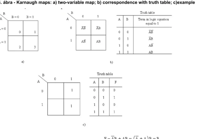
4.4. Two Variable Karnaugh Maps
The two-variable K-map contains four cells, covering all possible combinations of the two variables as is shown in Figure 1.4. Each row of the truth table corresponds to exactly one cell.
If the truth table row is one the respective cell contains a one. Usually the zeros are not indicated, and an empty cell is considered to contain a zero. Figure 1.4 a presents also the numbering of K-maps cells. Figure 1.4 c shows a two variable logic function truth table and the corresponding K-map. The logic function would be 1 if
A = 0 AND B = 1 OR A = 1 AND B = 1.
If the row or column of the map in which the 1 appears is labeled by a 1, the variable appears uncomplemented, otherwise the variable appears complemented. Read through the K- map cells content, the function expression is:
1.4. ábra - Karnaugh maps: a) two-variable map; b) correspondence with truth table; c)example
1.5. ábra - Karnaugh map; F=B
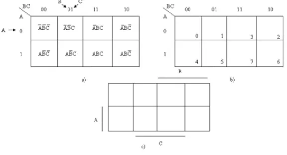
4.5. Three - Variable Karnaugh Maps
The K-maps edges are headed using a one-step (Gray) code.
The Gray code is a series of 2N code words, each of N-bits, in such a sequence that any adjacent code words differ only in one bit, including the first and last words too (cyclic property).
For example, in case of N = 2 the sequence of code words is:
(00), (01), (11), (01)
The Hamming distance of two code words of equal length is the number of positions at which the corresponding codes are different. For example, 10110 and 01101 differ in 4 positions, the distance between them is 4.The Hamming distance between any two adjacent code words of the Gray code is one (see Table 2.4).
When K-maps involve three variables; the cells represent the minterms of all variables, as is shown in Figure 1.6 a. The numbering of K-maps cells is presented in Figure 1.6 b. In Figure 1.6 c those columns and row are signed where the corresponding variables have logic-1 value.
Top cells are adjacent to bottom cells. Left-edge cells are adjacent to right-edge cells. Rows and columns on the opposite sides are also adjacent.
In the process of contraction and minimization the following steps and rules are necessary:
• introduce ones in each cell of the K-map for which the corresponding minterm in the function is equal to one.
• group adjacent cells which contain ones. The number of cells in a group must be a power of 2.
• the process is continued until no more variables can be eliminated by further contractions. The groups cover all cells containing ones.
1.6. ábra - Three-variable Karnaugh maps
In the case of three variables K-map:
• If a group of four adjacent cells (in-line or square) is contracted, the result yields in a single variable.
• If a group of two adjacent cells is contracted, the result yields in a two-variable product term.
• A single cell which cannot be combined represents a three-variable term.
1.7. ábra - Karnaugh map for Example 1.1 a
b.
1.8. ábra - Karnaugh map for Example 1.1 b
Figure 1.8 shows a split rectangular grouping and a single cell which cannot be combined (represents a three-variable term). The simplified expression is:
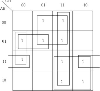
In Figure 1.9 the optimal grouping of 1-cells are shown. The minimal sums for K maps are given.
1.9. ábra - Grouping on three-variable Karnaugh maps
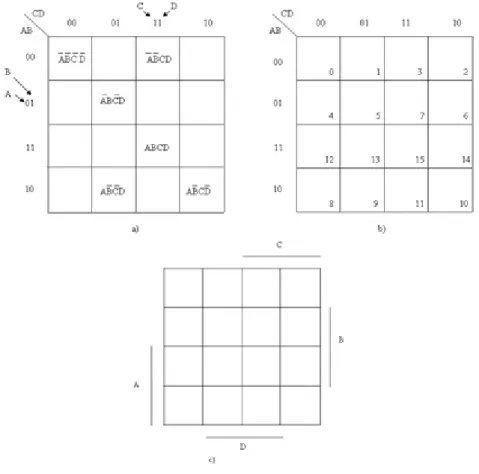
4.6. Four-Variable Karnaugh Maps
A four-variable map has 16 cells, as shown in Figure 1.10. The grouping rules are the same as for three variables K map. The goal is to find the smallest number of the largest possible sub cubes that cover the 1-cells.
1.10. ábra - Four-variable Karnaugh maps
Example 1.2 Use the K-map to simplify the logic function given by the minterms
The corresponding Karnaugh map is given in Figure1.11.
1.11. ábra - Karnaugh map for Example 1.2
The simplified expression is
The obtained terms are called the function prime implicants. If a minterm of a function is included in only one prime implicant, then this prime implicant is an essential prime implicant of the function [7].
In this way the K-maps permit the rapid identification and elimination of potential race hazards. The simplification result may not be unique.
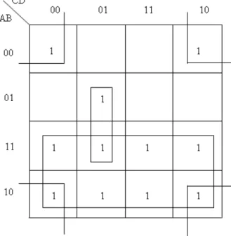
Example 1.3 Simplify the Karnaugh-map shown in Figure 1.12.
1.12. ábra - Karnaugh map for Example 1.3
The simplification result consists of 6 prime implicants:
Essential prime implicants for minimum cover
4.7. Karnaugh Map for Minimalization of a Four Variables Logic Function Expressed in Product-Of-Sums
Sometimes the Product-Of-Sums form of a function is simpler than the Sum-of Product form. In a very similar way as in the previous subsection (Four-Variable Karnaugh Maps), two adjacent maxterms can be contracted to a single sum. The involution identity is applied for the logic function: . In the minterm K-map the simplifications are made using zeros, obtaining the minimalization of .
Example 1.4 K-map method: contracting zeros (second “optimum” solution for the function given in Example 1.2) Use the - map to simplify the logic function given by the minterms
The corresponding Karnaugh-map is given in Figure1.13.
In the next the following rule is used: Replace F by , and 0’s become 1’s and vice versa.
1.13. ábra - Karnaugh map for Example 1.4
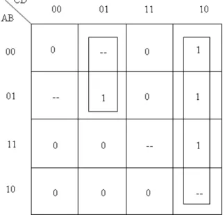
4.8. Incompletely Specified Logic Function
In the expression of incompletely specified logic function are such input combinations to which the Boolean function is not specified. The function value for these combinations is called don't care and the combination is called don’t care condition.
In an implementation the don’t care terms value may be arbitrarily 0 or 1. The selection point of view is if they are able to generate prime implicants in order to obtain the most advantageous solution.
Don’t care conditions are indicated on the K- maps by dash entries. Figure 1.14 shows a Karnaugh map involving don’t care conditions.
1.14. ábra - Karnaugh map with don’t care conditions
The map of Figure 1.14 can be used to obtain a minimal sum:
5. Combinational Logic Networks
Logic networks are implemented with digital circuits, and in reverse, digital circuits can be described and modeled with logic networks. For the analysis and synthesis of logic network the Boolean algebra is used.
The logic network (logic circuit) processes the actual values of the input variables (A, B, C, ...) and produces accordingly the output logic functions (F1, F2, ...).
Logic networks described by truth tables or Boolean expressions can be classified into two main groups:
1. Combinational networks: the output values depend only on the present input variable values;
2. Sequential networks: the output values depend on both the inputs to the operation and the result of the previous operation. Networks having the memory property will be studied in subsection “Sequential Logic Networks”.
The combinational logic network is the simplest logic network. The logic operations on the input variables are performed ”instantaneously” and the result will be available on the output at the same time, (except for the time delay due to the internal operation of the circuits). The output variables can be represented as logic functions of the input variables. Figure 1.15 shows a combinational logic network as a black box.
1.15. ábra - Combinational logic network
The combinational circuit maps an input (signal) combination to an output (signal) combination. The same input combination always implies the same output combination (except transients).
The reverse is not true. For a given output combination different input combinations can belong.
Combinational circuit examples: binary arithmetic circuits (half-adder, full-adder, etc.) (see subsection “Binary Arithmetic”), binary-coded-decimal code (BCD) – seven segment display (see subsection “Binary Codes and Decimal Arithmetic“), various encoders and decoders, multiplexers and demultiplexers, comparators (see subsection “Functional Blocks”), etc.
The combinational circuits are the interconnections of a large number of switches called logic gates.
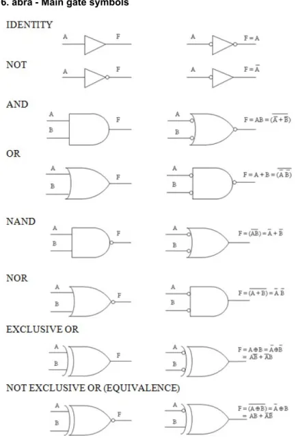
While the NOT, AND, OR functions have been designed as individual circuits in many circuit families, by far the most common functions realized as individual circuits are the AND-NOT (NAND) and OR-NOT (NOR) circuits. A NAND can be described as equivalent to an AND element driving a NOT element. Similarly, a NOR is equivalent to an OR element driving a NOT element. The reason for this strong bias favoring inverting outputs is that the transistors which preceded it are by nature inverters or NOT-type devices when used as signal amplifiers.
1.16. ábra - Main gate symbols
5.2. The EXCLUSIVE OR and NOT EXCLUSIVE OR Functions
The final two gates symbols introduced in Figure 1.16 are the EXCLUSIVE OR gate and the NOT EXCLUSIVE OR (Equality) gate. The EXCLUSIVE OR, (XOR) called the modulo-2- sum or “antivalency” operation is denoted by the symbol . The EXCLUSIVE OR function forms are:
By definition the value of is logic-1 if and only if A and B variables have different values. The complement of the EXCLUSIVE OR operation is the NOT EXCLUSIVE OR (called EXCLUSIVE NOR, XNOR or “equivalency”) operation. Their expressions are:
By definition the value of is logic-1 if and only if A and B variables have the same values. The EXCLUSIVE OR and NOT EXCLUSIVE OR gates are typically available with only two inputs.
The commercial gates (exception NOT) are often designed for multiple inputs. Generalized symbol shown in Figure 1.17 is frequently used when a single gate has several inputs.
1.17. ábra - AND gate with 8 inputs
The IEEE standard specifies two different types of symbols for logic gates [8]: the distinctive- and rectangular-shape symbols. Figure 1.16 shows the main distinctive-shape symbols and Figure 1.18 compares the AND and NAND gate symbols. Both of them are frequently used and the standard says that it has no preference between them. Since most digital designers and computer-aided design (CAD) systems prefer the distinctive-shape symbols, these symbols are used in this book.
1.18. ábra - Example for distinctive and rectangular shape logic symbols
5.3. Standard Forms for Logic Functions, Synthesis Using Standard Expressions and the Corresponding Circuits with NAND or NOR Gates
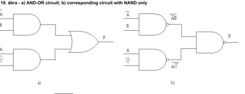
All logic functions can be specified using AND, OR and NOT operations. Both canonical forms: Sum of Products (SOP) and Product of Sums (POS) can specified and implemented by two-level AND-OR or OR-AND gate networks, respectively. Because the AND, OR and NOT operations can be implemented using either only NAND or only NOR gates, then based on the respective canonical forms all logic functions can be implemented with homogeneous two-level NAND or NOR gate networks. Consider the sum-of-products expression:
The two-level AND-OR circuit consists of a number of AND gates equal to the number of terms followed by a single OR gate. The logic circuit is shown in Figure 1.19 a. Next we apply De Morgan’s theorem to the above function
and therefore . The corresponding circuit with NAND gates is shown in Figure 1.19 b.
1.19. ábra - a) AND-OR circuit; b) corresponding circuit with NAND only
Although, the expression looks more complicated than , the circuit built up from NAND gates (Figure 1.19 b) has the advantage that is built up from the same gate types and consists of less transistors. If we start with a product-of-sums expression, the resulting circuit will be a two-level OR-AND structure. If the POS expression is:
Using De Morgan’s theorems, we can transform the expression as follows:
Hence
The POS function two-level OR-AND structure and the corresponding NOR circuit is shown in Figure 1.20.
1.20. ábra - a) OR-AND circuit; b) corresponding circuit with NOR only
5.4. Problems
1. Simplify the following expressions as far as possible:
a.
b.
c.
2. For three logic variables prove the identity:
3. Evaluate the following expressions for A = B = C = 1; D = 0; E = 1 a.
5. Write a Boolean expression for the logic diagram shown below:
6. Find the simplest expressions in the following Karnaugh maps:
2. fejezet - Number Systems
In digital computers the information is represented in a string of ON and OFF states of logic variables, a series of logic-1s and logic-0s. This chapter covers the positional number systems (decimal, binary, octal, and hexadecimal), the number conversions, representations of integer and real numbers and arithmetic operations. Various codes and the code conversion are studied. Finally, encoders, decoders, multiplexers, demultiplexers and various comparators are discussed.
1. Positional Number Systems
In the positional number system, or so called radix-weighted positional number system the value of a number is a weighted sum of its digits. The value associated with a digit is dependent on its position. In general, the numbers, in the base r (radix) system are of the form:
Where: r is the base of the number system, j, j-1,…,-(k-1),-k scalars, natural numbers between 0 and r − 1, inclusive.
1.1. Decimal Number System
The well known decimal system is just one in the class of number systems which belongs to the weighted positional number system. The decimal system is the most commonly used in our daily arithmetic. The numbers in combination of 10 symbols (digits) are called the decimal number system. This is a grouping system based on the repetition of symbols to note the number of each power of the base, in this case 10. The distinct digits (0 – 9) are multiplied by the power of 10, and it is significant that the position occupied by each digit. “.” is called the radix point. In the case of decimal number 356.21:
1.2. Binary Number System
In the binary system, the base is 2 (r = 2) and the symbols are 0 and 1. These numbers in positional code are expressed as power series of 2, and are called bits (binary digit).
In the expression
1.4. Conversion from decimal to binary
Several methods exist to convert from decimal to binary and vice versa. In the next two methods are presented:
Method 1 Descending Powers of Two and Subtraction
For numbers less then thousands, this method offers a very rapid and easy technique. The steps are:
• Find the greatest power of 2 that is close and less than the decimal number, and after that calculate the difference between them.
• Choose a next (lower) power of 2 which is close and less than the subtraction result.
• Repeat the above mentioned operations until the sum of the powers of 2 will give the decimal number. The binary answer is composed from 1s in the positions where the power of 2 fit into the decimal number and 0s otherwise.
For example, find the 156 decimal number binary equivalents. We list the power of 2 s and we “build” the corresponding number.
Method 2 Division by Two with Remainder
If the number has a radix point, as a first step, it is important to separate the number into an integer and a fraction part, because the two parts have to be converted differently.
The conversion of a decimal integer part to a binary number is done by dividing the integer part to 2 and then writing the remainders (0 or 1). Proceed with all successive quotients the same way and accumulate the remainders.
For example, find the 56 decimal number binary equivalent:
Number divided by 2 Result Remainder 56/2 28 0 LSB
28/2 14 0 14/2 7 0 7/2 3 1
3/2 1 1 1/2 0 1 MSB
The conversion of a decimal fraction part to a binary number is done by multiplying the fractional parts by 2 and accumulating integers.
For example, find the 0.6875 decimal number binary equivalent:
Number multiplying by 2 Integer Result 0.6875 x 2 = 1 0.3750
0.3750 x 2 = 0 0.7500 0.7500 x 2 = 1 0.5000 0.5000 x 2 = 1 0.0000
And
1.5. Octal and Hexadecimal Numbers
Positional number systems with base 8 (octal) and base 16 (hexadecimal) are used in digital computers.
In octal system the eight required digits are 0 to 7, and the radix is 8.
The hexadecimal system (base 16) uses sixteen distinct symbols: numbers from 0 to 9, and letters A, B, C, D, E, F to represent values between ten to fifteen.
1.6. Conversion from octal or hexadecimal to decimal
The conversion is similar to the previous subsection Method 2. This approach is called: Division by Eight or Sixteen with Remainder. Here the numbers in the positional code are expressed as power series of 8 and 16.
1.7. Conversion from octal and hexadecimal to binary
For example, to convert from binary to octal, the binary number three bit groups were separated, that could be converted directly:
011 010 111 . 001 binary number 3 2 7 . 1 octal equivalent Vice versa:
4 5 6 . 2
100 101 110 . 010
To convert from hexadecimal to binary and reverse, the binary number four bit groups were separated, that could be converted directly:
1010 0010 11012 = A2D16 7F316 = 0111 1111 00112
The non-positional number systems uses for example Roman numerals (I = 1, V = 5, X = 10, L = 50, C = 100, D = 500 and M = 1000).
2. Binary Arithmetic
Arithmetic operations with numbers in base r follow the same rules as for decimal numbers. The addition, subtraction, multiplication and division can be done in any radix-weighted positional number system.
In digital computers arithmetic operations are performed with the binary number system (radix = 2). The binary system has several mathematical advantages: i.e. easy to perform arithmetic operations and simple to make logical decisions. The same symbols (0 and 1) are used of arithmetic and logic.
Now we will review the four basic arithmetic operations, then the handling of the case of negative (signed) numbers.
2.1. Binary Addition
The algorithm of binary addition is similar to that of decimal numbers: aligning the numbers with the same radix, starting the addition with the pair of least significant digits. The half adder adds two single binary digits A and B. It has two outputs, sum (S) and carry (C). The rules for two-digit binary addition are the following:
A B Sum Carry 0 + 0 = 0 0 1 + 0 = 1 0 0 + 1 = 1 0
1 + 1 = 0 1 (to the next more significant bit) The half adder logic diagram is shown in Figure 2.1.
2.1. ábra - Half adder logic diagram
The rules of binary addition (without carries) are the same as the truths of the EXCLUSIVE OR (XOR [http://academic.evergreen.edu/projects/biophysics/technotes/program/
logic.htm#gates]) gate [9]. Circuit implementation requires 2 outputs; one to indicate the sum and another to indicate the carry. Two digits (bits) at the actual position and the carry from the previous position should be added. The process is then repeated. The full adder is a fundamental building block in many arithmetic circuits, which adds three one-bit binary numbers (C, A, B) having two one-bit binary output numbers, a sum (S) and a carry (C1).
C A B S C1 0 + 1 + 0 = 1 0
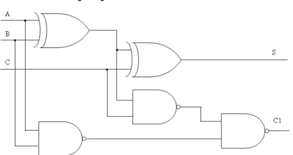
0 + 1 + 1 = 0 1 (to the next more significant bit) 1 + 1 + 0 = 0 1 (to the next more significant bit) 1 + 1 + 1 = 1 1 (to the next more significant bit) The full adder logic diagram is shown in Figure 2.2.
2.2. ábra - Full adder logic diagram
The following is an example of binary addition:
2.2. Binary Subtraction
In many cases binary subtraction is done in a special way by binary addition. One simple building block called adder can be implemented and used for both binary addition and subtraction.
Using the borrow method; the basic rules are summarized in the next:
Borrow A B Difference 0 0 - 0 = 0
0 1 - 0 = 1 0 1 - 1 = 0
0 0 - 1 = 1 and borrow 1 from the next more significant bit
1 0 - 0 = 1 and borrow 1 from the next more significant bit 1 0 - 1 = 0 and borrow 1 from the next more significant bit 1 1 - 0 = 0
1 1 - 1 = 1 and borrow 1 from the next more significant bit
When a larger digit is to be subtracted from a smaller digit it is necessary to “borrow” from the next-higher-order digit position. The following example illustrates binary subtraction:
2.3. Binary Multiplication
The rules for two-digit binary multiplication are the next:
A B Product 0 x 0 = 0 1 x 0 = 0 0 x 1 = 0
1 x 1 = 1 and no carry or borrow bits
The rules of binary multiplication are the same as the truths of the AND gate [9]. In a very similar way to the decimal multiplication an array of partial products are formed and binary added. The following is an example of binary multiplication:
1 1.12 Multiplicand x 1 0 12 Multiplier ---
--- 1 0 0 1.12 Product
2.4. Binary Division
Binary division is the repeated process of subtraction, just as in decimal division [9]. A trial quotient digit is selected and multiplied by the divisor. The product is subtracted from the dividend to determine whether the trial quotient is correct. The principle of binary division is seen by the next example:
3. Signed Binary Numbers
The positive integers and the number zero can be represented as unsigned binary numbers using an n-bit word. When working with any kind of digital electronics in which numbers are being represented, it is important to distinguish both positive and negative binary numbers. The three representations of signed binary numbers will be discussed in the next. These approaches involve using one of the digits of the binary number to represent the sign of the number [10].
3.1. Sign-Magnitude Representation
To mark the positive and negative quantities instead of using plus and minus sign we will use two additional symbols 0 and 1. In this approach the information’s left bit (the most-significant bit, MSB) is the sign bit, where 0 denotes positive and 1 denotes negative value. The rest of the bits represent the number magnitude. This method is simple to implement, and is useful for floating point representation. The disadvantage of sign-magnitude representation is that the sign bit is independent of magnitude, and mathematical operations are more difficult. It is very important to not confuse this representation with unsigned numbers! Table 2.1 illustrates this concept, including all three representations of signed binary numbers using 4 bits.
Here, the MSB bit (sign bit) is separated from the remaining 3 bits which denote the magnitude in the binary number system. It can be noted that 0 has two different representations, and can be both + 0 and – 0!
3.2. 1’s-Complement Representation
The simplest of these methods is called 1’s complement, which can be derived by just inverting all the bits in the number. Reversing the digits, by changing all the bits that are 1 to 0 and all the bits that are 0 to 1 is called complementing a number. The positive numbers 1’s complement representation is the same as in the sign-magnitude approach and the 0 has again two different representations. In this approach the MSB bit also shows the sign of the number (all of the negative values begin with a 1, see Table 2.1).
3.3. 2’s-Complement Representation
The 2's complement number representation is most commonly used for signed numbers on modern computers. An easier way to compute the 2’s complement of a binary integer is to consider the 1’s complement of the number plus 1. The 8 bit representations of the integer number – 9 are:
Signed-Magnitude representation: 1|0001001 1’s complement: 1|1110110
2’s complement: 1|1110110 + 1
1|1110111
For further examples using 4 bits see Table 2.1.
Three representations of signed binary numbers using 4 bits Signed decimal Sign-magnitude 1’s complement 2’s complement equivalent representation representation representation +7 0 111 0 111 0 111
+6 0 110 0 110 0 110 +5 0 101 0 101 0 101 +4 0 100 0 100 0 100 +3 0 011 0 011 0 011 +2 0 010 0 010 0 010 +1 0 001 0 001 0 001
-4 1 100 1 011 1 100 -5 1 101 1 010 1 011 -6 1 110 1 001 1 010 -7 1 111 1 000 1 001 -8 --- --- 1 000
3.4. Addition with 2’s Complement Representation
If the complement representation of signed numbers is used there is no need for both adder and subtractor unit in a computer.
Let’s assume two n-bit signed numbers M and N represented in signed 2’s complement format. The sum M + N can be obtained including their sign bits to get the correct sum. A carry out of the sign bit position is discarded. In the next, addition in the 2‘s complement representation examples are given (using 5 bits).
If the sum of two n-bit numbers results in an n + 1 number an overflow appears. The first step in the detection of such an error is the examination of the sign of the result. The overflow detection can be implemented using either hardware or software, and depends on the signed or unsigned number system used.
4. Binary Codes and Decimal Arithmetic
The binary number system, handling only two digit symbols, is the simplest system for a digital computer. From the user point of view it is easy to compute and operate with decimal numbers. A combination of binary and decimal approaches, keeping their advantages, result in a system in which the digits of the decimal system are coded by groups of binary digits.
The basic concept is to convert decimal numbers to binary, to perform all arithmetic calculations in binary, and then convert the binary result back to decimal.
The best known scheme to code the decimal digits is the 8421 binary-coded-decimal (8421 BCD) scheme. In this weighted code 10 decimal digits are represented by at least 4 binary digits. In 8421 BCD code each bit is weighted by 8, 4, 2 and 1 respectively. For example the 8421 BCD representation of the decimal number 3581 is 0011 0101 1000 0001.
Beside 8421 BCD code other weighted codes have been used. These codes have fixed weights for different binary positions. It has been shown in [11] that exist 17 different set of weights possible for a positively weighted code: (3,3,3,1), (4,2,2,1), (4,3,1,1), (5,2,1,1), (4,3,2,1), (4,4,2,1), (5,2,2,1), (5,3,1,1), (5,3,2,1), (5,4,2,1), (6,2,2,1), (6,3,1,1), (6,3,2,1), (6,4,2,1), (7,3,2,1), (7,4,2,1), (8,4,2,1). It is also possible to have a weighted code in which some of the weights are negative, as in the 8, 4, -2, -1 code shown in Table 2.2.
Binary codes for the decimal digits Decimal 8421 Excess-3 2-out-of-5 digit binary code code code 0 0000 0011 11000 1 0001 0100 00011 2 0010 0101 00101 3 0011 0110 00110 4 0100 0111 01001 5 0101 1000 01010 6 0110 1001 01100 7 0111 1010 10001 8 1000 1011 10010 9 1001 1100 10100
This code has the useful property of being self-complementing: if a code word is formed by complementing each bit individually (changing 1's to 0's and vice versa), then this new code word represents the 9's complement of the digit to which the original code word corresponds [12].
The non-weighted codes don’t have fixed weights for different binary positions. For example the excess-3 code is derived by adding 00112 = 310 to the 8421 BCD representation of each decimal digit. The 2-out-of-5 code shown in Table 2.2 has the property that each code word has exactly two 1's.
4.1. Decimal Addition Using 8421 BCD Code
The 8421 BCD code is widely used and it is simplified as BCD code. Because of the popularity of this code in the next the addition operation is presented.
Addition is performed by individually adding the corresponding digits of the decimal numbers expressed in 4-bit binary groups starting from right to left. [13]. If the result of any addition exceeds nine (1001) then the number six (0110) must be added to the sum to account for the six invalid BCD codes that are available with a 4-bit number.
Perform the following decimal additions (24 + 15) in BCD code.
Consider the following addition: 28 + 59. When the sum of the LSB digits of the two numbers (8 + 9) is greater than 15 it is necessary to introduce a correction. In this approach a correct code group results but with an incorrect sum.
4.2. 7-Segment Code
A very useful decimal code is the 7-segment code which is able to show numeric info on seven-segment displays. The 7-segment display (see Figure 2.3) consist of 7 LEDs (light emitting diodes), each one controlled by an input where 1 means “on”, 0 means “off”. The decimal digit and the corresponding 7-segment code are shown in Table 2.3.
2.3. ábra - 7-segment display
4.3. Gray Code
The most useful unit distance code is the Gray code which is shown in Table 2.4. This unweighted code has such a sequence that any adjacent code words differ only in one bit (see subsection “Minimization of Logic Functions” Three - Variable Karnaugh Maps). The attractive feature of this code is the simplicity of the algorithm for translating from the binary number system into the Gray code. [12]
2.4 táblázat The 3 bit Gray code
This algorithm is described by the expressions:
Unit-distance codes, which could minimize errors, are used in devices for converting analog or continuous signals such as voltages or shift rotations into binary numbers which represent the magnitude of the signal. Such a device is called an analog-digital converter [12].
4.4. Error Detection
In general data transfer between various parts of a computer system, the transmission over communication channels or their storage in memory is not completely error free. For the purpose of increasing system reliability, special features are included in many digital systems, i.e. to introduce some redundancy in encoding the information handled in the system. For example, the error detecting properties of the 2-out-of-5 code is based on its feature to have exactly two 1’s within a code group. Not all codes have error detecting capability.
A simple error detecting method is the calculus of a parity bit, which is then appended to original data. The parity type could be: even or odd. The parity bit is added to each code word so as to make the total number of 1's in the resultant string even or odd. [14].
For example, when the parity type is even, the result is an even number of 1’s 100 0100→0 100 0100
110 0100→1 100 0100
In data transmission, the sender adds the parity bit (message bit) to the existing data bits before forwarding it which is compared to the expected parity (check bit) calculated from the receiver.
Generating even parity bit is just an XOR function. In a similar way, generating odd parity bit is just an XNOR function.
To minimize the disadvantages of this single error detection method (cannot determine which bit position has a problem) the following rules have to be observed. The necessary and sufficient conditions for any set of binary words to be a single-error-correcting code is that the minimum distance between any pair of words be three [12].
In general, if the Hamming distance is D (see subsection “Minimization of Logic Functions”), Hamming Distance is equal to the number of bit positions in which 2 code words differ), [14] to detect k-single bit error, minimum Hamming distance is
D (min) = k + 1
The Hamming Code is a type of Error Correcting Code (ECC) which adopts parity concept, having more than one parity bit, providing error detection and correction mechanism. To correct k errors D (min) = 2k + 1 is required.
4.5. Alphanumeric Codes
Several codes have been proposed to represent numeric information and various characters. The nonnumeric ones are called alphanumeric codes. The characters are for example:
alphabet letters, special symbols, punctuation marks, special control operations. The commonly used alphanumeric code is the American Standard Code for Information Interchange (ASCII). The 7-bit version of this code is frequently completed with an eighth bit, the parity bit.
Another encoding, Unicode is a computing [http://en.wikipedia.org/wiki/Computing] industry standard [http://en.wikipedia.org/wiki/Technical_standard] for the consistent encoding [http://
en.wikipedia.org/wiki/Character_encoding] [15]. It can be implemented by so called UTF-8 [http://en.wikipedia.org/wiki/UTF-8], UTF-16 [http://en.wikipedia.org/wiki/UTF-16] character encodings. For example UTF-8 uses one byte [http://en.wikipedia.org/wiki/Byte] for any ASCII [http://en.wikipedia.org/wiki/ASCII] characters, and up to four bytes for other characters.
5. Functional Blocks
The traditional process of logic synthesis is based on the application of logic gates. Its more modern variant makes the use of a composition of smaller, simpler circuits and programmable logic devices. However in many cases it is more advantageous to use a logic synthesis procedure based on the application of logic functional blocks.
In this subsection we will give an overview of some important and useful basic combinational functional blocks. In order to design new circuits, design hierarchy, the so called Top-Down, Bottom-Up, Meet in the Middle Design Approaches or Computer-Aided Design (CAD) tools could be used [16].
5.1. Code Converter
A code converter is an important application of combinational networks (see subsection “Combinational Logic Networks”). Such a digital system is able to transform information from one code to another. For example a BCD-to-Excess-3 code converter is useful in digital arithmetic [16]. To understand the „machine language” a set of code conversions has to be applied. Figure 2.4 shows a possible application, where a signal in Gray code transmitted by a position sensor is received by a Gray-Binary converter (a typical application for Gray code is in absolute position sensing) and the result is converted in normal (8421) BCD code. At the end, the display unit applies BCD to 7-segment code conversion. In this way the
Code converters are typically multiple input-multiple output combinational circuits. They can be realized by appropropriate gate networks or using Read only Memories.
5.2. Binary Decoders
A combinational circuit that converts binary information from n coded inputs to a maximum 2n coded outputs is called n-to-2n decoder, more generally n-to-m decoder, m ≤ 2n [17]. Figure 2.5 shows a binary decoder as a black box.
2.5. ábra - Binary decoder as a black box
Enable input (E): it must be on (active) for the decoder to function, otherwise its outputs assume a single ”disabled” output code word.
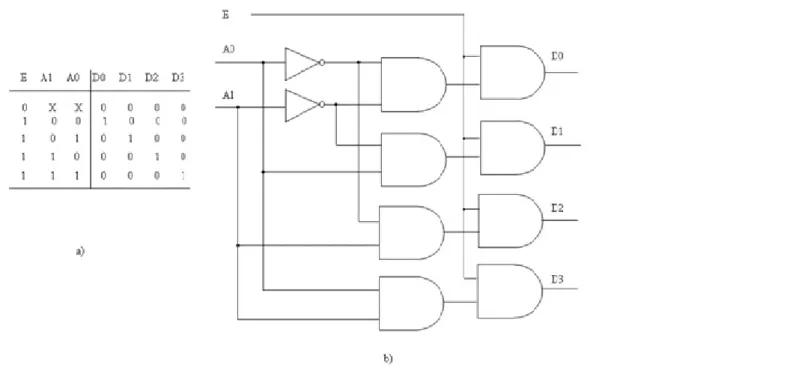
5.3. 2-to-4 Decoder
In a 2-to 4 decoder, 2 inputs, A0, A1 are decoded into 22 = 4 outputs, D0 through D3. Each output represents one of the minterms of the 2 input variables. The truth table and the logic circuit without Enable input are given in Figure 2.6.
2.6. ábra - 2-to-4 line decoder without Enable; a) truth table, b) gate level logic diagram
Decoder output lines implement minterm functions. Any combinational circuit can be constructed using decoders and OR gates [18]. The 2-to-4 decoder truth table and the logic circuit with Enable input are given in Figure 2.7. In this case the additional gate level produces time delay, which can be avoided by using 3 input AND gates instead of 2 input AND gates in Figure 2.6 b.
2.7. ábra - 2-to-4 line decoder with Enable a) truth table; b) gate level logic diagram
Decoder expansion means to construct larger decoders from small ones. The next example (see Figure 2.8) shows the interconnection of two 2-to-4 decoders in order to have the required 3-to-8 decoder size. If A2 = 0: enables top decoder, when A2 = 1: enables bottom decoder.
2.8. ábra - 3-to-8 decoder from 2-to-4 decoders
5.4. Binary Encoders
An encoder is a multi-input combinational logic circuit that executes the inverse operation of a decoder. In general, it has 2n input lines and n output lines. The output lines generate the binary equivalent of the input line whose value is 1 [19]. Figure 2.9 shows a binary encoder as a black box.
2.9. ábra - Binary encoder as a black box
If the enable signal E = 0 then all outputs are 0 else Yj = F (X0, X1,…,X2n -1),
j = 0...n-1. If the valid signal is equal to 1 (V = 1) the valid code is present at the outputs; otherwise V = 0.
5.5. 4-to-2 Encoder
Using a 4-to-2 encoder, 4 inputs, D0 - D3 are encoded into 2 outputs, A0 and A1. The truth table and the logic circuit without Enable input are given in Figure 2.10.
2.10. ábra - 4-to-2 line encoder without Enable truth table and gate level logic diagram
5.6. Priority Encoders
2.11. ábra - Priory encoder truth table and logic circuit
5.7. Multiplexer (MUX)
Multiplexers work as selectors, which choose one input to pass through to the output. A 2 x 1 multiplexer has two data inputs (I0 and I1), one select input S and one data output (D). Figure 2.12 a) shows the internal structure of a two input MUX. At the output of the simple AND - OR combinational circuit if S = 0, appears the I0 value, and if S = 1, I1’s input value passes through.
In general, an M x 1multiplexer has M data inputs, log2 (M) select inputs, and one output. Using another notation, if M = 2n, the 2n-to-1 multiplexer works with 2n data inputs, n select inputs and one output.