Figure 3-0.
Table 3-0.
Listing 3-0.
Overview
The TigerSHARC® processor’s 32-bit address bus gives it an address space of four gigawords. This address space is common to a cluster of Tig- erSHARC® processors that share the same cluster bus. This chapter defines the memory map of each TigerSHARC® DSP in the system, where the memory space defines the location of each element. The zones in the memory space are made up of the following regions:
• Host address space
• External memory bank space—the region for standard addressing of off-chip memory
• External multiprocessor space—the on-chip memory of all other TigerSHARC® DSPs connected in a multiprocessor system
• Internal address space—the region for standard internal addressing
The global memory map is shown in Figure 3-1 below.
Figure 3-1. Global Memory Map
0x00000000 0x0000FFFF 0x00080000 0x0008FFFF 0x00100000 0x0010FFFF 0x00180000 0x001807FF
Internal Memory 0 Internal Memory 1 Internal Memory 2 Internal Registers
0x00000000 0x003FFFFF 0x01C00000
Internal Memory
Broadcast 0x02000000 Processor ID 0 0x02400000 Processor ID 1 0x02800000 Processor ID 2 0x02C00000 Processor ID 3 0x03000000 Processor ID 4 0x03400000 Processor ID 5 0x03800000 Processor ID 6 0x03C00000 Processor ID 7 0x04000000
0x10000000
0x0C000000
0x08000000 SDRAM
Memory Block 0 Memory Block 1
INTERNAL SPACE Host
GLOBAL SPACE
RESERVED
RESERVED RESERVED RESERVED
RESERVED
Host Address Space
The host address space is the space defined for the host when it is accessed as a slave. When referring to this space, the pipelined or asynchronous protocol is used according to the host bits in the SYSTAT register—see page 3-51. The backoff is also effective on this zone—see “Backoff” on page 6-86.
The host address space is 3.75 gigawords and is divided into two fields:
External Memory Bank Space
Normal external accesses are split into three zones. One zone is for SDRAM; the access is executed in SDRAM protocol. The other two zones are identified by external memory select pins MS0 and MS1, where the access protocol is pipelined, and the parameters are defined by the SYSCON regis- ter value—see section “Bus Control/Status (BIU) Register Group” on page 3-47.
Table 3-1. Host Address Space
Bit # Name Definition
Bits[27:0] ADDRESS Address in host range.
Bits[31:28] Not 0000 Determine the type of address.
As long as the value is not 0000, the address is directed to the host address space:
0b0001 – 0b1111: Host 0b0000: Others
The external memory bank space is divided into three fields, as illustrated below:
Multiprocessor Space
The multiprocessing space maps all the internal memory space of each of the TigerSHARC® DSPs in the cluster into any other TigerSHARC®
processor. Each TigerSHARC® DSP in the cluster is identified by its ID (which is between 0 and n-1 where n is the number of TigerSHARC®
processors in the system).
The external multiprocessor space is divided into three fields, as illustrated in Table 3-3:
Table 3-2. External Memory Bank Space
Bit # Name Definition
25:0 ADDRESS Address
27:26 MS Memory Select – select the memory bank:
00…internal or multiprocessor space 01…SDRAM
10…MS0 11…MS1
31:28 ≠0000 Determine the type of address as host space.
Table 3-3. External Multiprocessor Space
Bit # Name Definition
21:0 ADDRESS Internal address space, as described in “Internal Address Space” on page 3-5.
Note: A TigerSHARC® DSP’s own Internal space can be accessed via the multiprocessing space for write transactions only. This, how- ever, is performed through the external bus and should only be used in special cases where data must pass through the Tiger- SHARC® DSP bus interface.
Internal Address Space
The internal address space is described by bits [21:0] of multiprocessing or internal space. The internal address space is divided into three fields, as illustrated below:
25:22 PRID Processor ID – determine the target processor:
1NNN… Defines one of eight possible processors, where NNN is the target TigerSHARC® DSP ID.
0111 Broadcast—i.e., access (which can be only write) is to all TigerSHARC® DSPs in the cluster.
0000 Defines the memory bank as internal.
31:26 000000 Determine a multiprocessing or internal space.
Table 3-4. External Multiprocessor Space
Bit # Name Definition
18:0 ADDRESS Address
21:19 ISPACE Internal Space – determines the internal space:
000… Block 0 001… Block 1 010… Block 2
011… Internal Registers (Uregs) 1XX… Reserved
Table 3-3. External Multiprocessor Space
Bit # Name Definition
Internal space is the space for transactions within the TigerSHARC® DSP and access to this memory space is not reflected on the cluster bus. Inter- nal address space is used to access the internal memory blocks or any of the Universal registers (Uregs), the internal registers that are mapped to the TigerSHARC® DSP memory map. Most software accessible registers are Uregs.
Access to Uregs (ISPACE = 011) is only for multiprocessing space. Internal access to registers can not be memory mapped—in load/store instructions, for example, the address can not point to a register through the internal space. The DMA also can not access a register directly, although there is an exception, link receive DMA channels may write to other link transmit registers.
Register Groups
Registers can be accessed in two ways—either by core with a register access instruction, or by a different master as a memory-mapped register. Two fields, Ureg group and Ureg, can be used to access the register via a regis- ter access instruction:
The register space is composed of 64 register groups with up to 32 regis- ters in each group. Register groups are defined in the range 0x3F:0
(63:0), where groups 0x1F:0 are accessible by all transfer instructions (load immediate, move register, load and store), and groups 0x3F:0x20 are
31:22 0000 00 PRID Determines internal space
Table 3-4. External Multiprocessor Space
Bit # Name Definition
0000 00 PRID
31:22 21:19 18:11
011 00000000
10:5 4:0
Ureg group Ureg
accessible only by move register instructions and direct accesses of other masters.
Some of the registers do not use all 32 bits. The unimplemented bits are reserved, and should not be used. When writing to such a register, they must be set to zero. When reading such a register the unimplemented bits may be of any value.
The register groups are as follows:
• 0x00 – 0x09: Compute block register file different aliases
• 0x0C – 0x0F: Integer ALU registers
• 0x1A, 0x38 – 0x39: Interrupt and sequencer registers
• 0x30 – 0x37, 3B: Branch target buffer (BTB) registers
• 0x1B, 0x3D, 0x3E, 0x3F: Debug logic (0x3F reserved)
• 0x24, 3A: EP Control/Status registers
• 0x20 – 0x23: DMA registers
• 0x25 – 0x27: Link registers
• Others – RESERVED. These registers must not be accessed by applications since they could cause unexpected behavior by the TigerSHARC® DSP.
The register groups are described in the following sections.
Compute Block Register Files
The compute block register file is a 32-word register. There are two such register files, one in each of the compute blocks (X and Y). The register file is aliased in several groups, some of which are applicable for data trans- fer instructions only. Some groups point to compute block X and some to block Y; those that point to both compute blocks in parallel actually point to the same register.
Merged Access
One type of access to both X and Y register files is the merged access.
Merged access splits the data between the two compute blocks. If the data transfer is specified as a quad word, two words will be transferred to CBX and two will be transferred to CBY. If the access is long, one word will be transferred to CBX, and another will be transferred to CBY. This is illus- trated in Figure 3-2 on page 3-9.
Note: The transaction of a word to a merged group is illegal.
Figure 3-2. Merged and Broadcast Access to CBX and CBY
Figure 3-2 above shows the data split for merged CBX and CBY. The merged
CBY and CBX is the same, replacing X with Y and vice versa.
Broadcast Transfer
Another data transfer shown in Figure 3-2 is the broadcast transfer. The data are written to CBX and CBY simultaneously. Broadcast duplicates the data in both compute blocks and can only be used for write to compute registers.
w1 w0
w0 w1
w2 w3
w0 w1
w2 w3
w0 w1
w2 w3
w0 w1
w2 w3
w0 w1
w2 w3
Long word access
compute block X compute block Y Quad data access (two longs)
Source
compute block X compute block Y MERGED
Split data between two CB registers
BROADCAST Load same data to two CB registers
Quad data access (unit)
Source
compute block X compute block Y
The CB register types of accesses are listed in Table 3-5.
Unmapped Compute Block Registers
There are several registers in the compute block (CB) units that are not Universal registers (Uregs), in that they are not accessed in the same way that Uregs are accessed. These registers are accessed by regular CB instruc- Table 3-5. Compute Block RF Groups
Address Group Definition Ureg Group
0x180000 : 0x18001F Compute block X (CBX) register file reg- ular access
0b000000
Not accessible 1
1 Alternative access is only for load/store instruction - DAB, circular buffer.
Compute block X (CBX) register file reg- ular access alternative
0b000001
0x180040 : 0x18005F CBY register file regular access 0b000010 Not accessible 1 CBY register file regular access alternative 0b000011
0x180080 : 0x18009F CBX & CBY merged 0b000100
Not accessible 1 CBX & CBY merged alternative 0b000101
0x1800C0 : 0x1800DF CBY & CBX merged 0b000110
Not accessible 1 CBY & CBX merged alternative 0b000111 0x180100 : 0x18011F CBX & CBY broadcast 0b001000 Not accessible 1 CBX & CBY broadcast alternative 0b001001
tions that transfer the data between the unmapped registers and the general-purpose compute block Uregs. These registers are described below.
Global Registers—XSTAT/YSTAT Compute Block Status Registers
XSTAT and YSTAT are 32-bit compute block status registers that record the state of the CBX/Y flags. Every flag is updated when an instruction belong- ing to its unit is completed (that is, AZ, which is an ALU result of zero is updated on completion of ALU instructions).
These registers are accessed by the following compute block instructions:
• X/YRs = X/YSTAT—see the description of the Rs = X/YSTAT instruc- tion in the TigerSHARC DSP Instruction Set Specification
• X/YSTATL = Rm—transfers bits [14:0], see the description of the
X/YSTAT = Rm and X/YSTATL = Rm instructions in the TigerSHARC DSP Instruction Set Specification
• X/YSTAT = Rm—see the description of the X/YSTAT = Rm and
X/YSTATL = Rm instructions in the TigerSHARC DSP Instruction Set Specification
The following is recorded when the bit is set:
Table 3-6. Bit Descriptions
Bit Bit Name Description
0 AZ ALU zero
1 AN ALU negative
2 AV ALU overflow
3 AC ALU carry
4 MZ Multiplier zero
5 MN Multiplier negative
6 MV Multiplier overflow
7 MU Multiplier Underflow
8 SZ Shifter zero
9 SN Shifter negative
11:10 BF Block floating-point flags
12 AI ALU floating-point invalid operation
13 MI Multiplier floating-point invalid operation
14 TROV Trellis accelerator overflow
15 TRSOV Trellis accelerator sticky overflow
19:16 Reserved
20 UEN Underflow enable
21 OEN Overflow enable
22 IVEN Invalid enable
23 Reserved
24 AUS ALU floating-point sticky underflow
25 AVS ALU floating-point sticky overflow
26 AOS ALU fixed-point sticky overflow
27 AIS ALU floating-point invalid operation sticky
28 MUS Multiplier floating-point sticky underflow
29 MVS Multiplier floating-point sticky overflow
30 MOS Multiplier fixed-point sticky overflow
Table 3-6. Bit Descriptions (Continued)
Bit Bit Name Description
ALU Registers
The PR0 and PR1 are two 32-bit registers used for sideways sum instruc- tions. Use the following instructions to access these registers:
PR1:0; = Rmd
(see the PR1:0 = Rmd instruction in the TigerSHARC DSP Instruction Set Specification)
Rsd = PR1:0;
(see the Rsd = PR1:0instruction in the TigerSHARC DSP Instruction Set Specification)
Multiplier Registers
MR[3:0] and MR4 registers are used as accumulators for the different types of fixed-point MAC instructions (see “Fixed-Point MAC Operations” in the TigerSHARC DSP Instruction Set Specification). These registers are accessed by different multiplier instructions.
Shifter Registers
BFOTMP is a 64-bit register used in the PUTBITS instruction (see Rsd+=PUT-
BITS Rnd BY Rmd in the TigerSHARC DSP Instruction Set Specification) and accessed by the following instructions:
BFOTMP = Rmd;
Rsd = BFOTMP;
31 MIS Multiplier floating-point invalid operation sticky
Table 3-6. Bit Descriptions (Continued)
Bit Bit Name Description
Enhanced Communications Registers
Data Registers
The enhanced communications instructions use 16 data registers, TR0 through TR15. Each register is 32 bits wide.
Trellis History Registers
The Trellis history registers, THR0 and THR1, are 32-bit registers.
This register pair keeps the history of ACS selection decisions. On each ACS instruction execution THR1:0 are shifted right, and the selection vector (one bit for each ACS decision) is shifted into THR1:0 MSBs. The shift is by four in 32-bit operations, and by eight in 16-bit operations.
This register is also used for the bit representation of the spreading code and scrambling code in DESPREAD functions.
IALU Registers
Each IALU has two Ureg groups. The first group is the general-purpose reg- ister file, which includes 32 word registers each; the second group is the circular buffer register file, for the specific registers. The IALU register groups are listed in Table 3-7, “IALU RF Groups,” on page 3-15.
The circular buffer register files contain the following registers:
• 3:0: Circular buffer base registers JB[3:0] and KB[3:0]
• 7:4: Circular buffer length registers JL[3:0] and KL[3:0]
• 31:8: Reserved
Register J31: JSTAT
The JSTAT status register records the state of the JALU flags, and is updated as a result of various IALU instructions:
Register K31: KSTAT
The KSTAT status register records the state of the KALU flags and is identical to JSTAT except that the bits names are KZ, KN, KV and KC. KSTAT as a Ureg is mapped as register 31 (K[31]) in the KALU register group.
Table 3-7. IALU RF Groups
Address Group Definition Group
0x180180 : 0x18019F JALU register file 0x0C
0x1801A0 : 0x1801BF KALU register file 0x0D
0x1801C0 : 0x1801DF JALU circular buffer register file 0x0E 0x1801E0 : 0x1801FF KALU circular buffer register file 0x0F
Table 3-8. JSTAT Register Bit Descriptions
Bit # Name Definition
0 JZ JALU zero
1 JN JALU negative
2 JV JALU overflow
3 JC JALU carry
31:4 Reserved
Interrupt Control and Sequencer
Sequencer Register Groups
All sequencer registers (including the BTB address range) are accessible by single word access only.
The 32-bit register group 0x1A is dedicated to sequencer registers, inter- rupt control and status registers—see Table 3-9.
Table 3-9. Sequencer Registers
Group 0x1A - Reg #
Single Word Register Type Direct
Memory Address
Remarks
0x00 CJMP Address for computed branch (see the Tig- erSHARC DSP Instruction Set Specifica- tion)
0x180340 –
0x02 RETI Address for return from interrupt (see the TigerSHARC DSP Instruction Set Specifica- tion)
0x180342 –
0x03 RETIB Alias of RETI - –
0x04 RETS Return address for exception (see “Excep- tions” on page 5-21)
0x180344 –
0x05 DBGE Return address for emulation trap (see
“Exceptions” on page 5-21)
0x180345 –
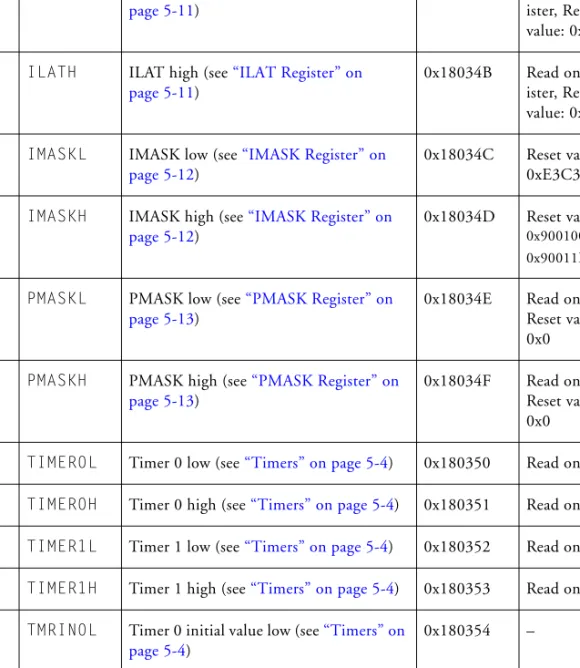
0x06 ILATSTL ILAT low set address 0x180346 Write only register 0x07 ILATSTH ILAT high set address 0x180347 Write only
register
0x8 LC0 Loop counter #0 0x180348 –
0x9 LC1 Loop counter #1 0x180349 – 0x0A ILATL ILAT low (see “ILAT Register” on
page 5-11)
0x18034A Read only reg- ister, Reset value: 0x0 0x0B ILATH ILAT high (see “ILAT Register” on
page 5-11)
0x18034B Read only reg- ister, Reset value: 0x0 0x0C IMASKL IMASK low (see “IMASK Register” on
page 5-12)
0x18034C Reset value:
0xE3C3C000 0x0D IMASKH IMASK high (see “IMASK Register” on
page 5-12)
0x18034D Reset value:
0x90010061 or 0x90011E61 1 0xE PMASKL PMASK low (see “PMASK Register” on
page 5-13)
0x18034E Read only;
Reset value:
0x0 0xF PMASKH PMASK high (see “PMASK Register” on
page 5-13)
0x18034F Read only;
Reset value:
0x0 0x10 TIMER0L Timer 0 low (see “Timers” on page 5-4) 0x180350 Read only 0x11 TIMER0H Timer 0 high (see “Timers” on page 5-4) 0x180351 Read only 0x12 TIMER1L Timer 1 low (see “Timers” on page 5-4) 0x180352 Read only 0x13 TIMER1H Timer 1 high (see “Timers” on page 5-4) 0x180353 Read only 0x14 TMRIN0L Timer 0 initial value low (see “Timers” on
page 5-4)
0x180354 –
0x15 TMRIN0H Timer 0 initial value high (see “Timers”
on page 5-4)
0x180355 –
Table 3-9. Sequencer Registers (Continued)
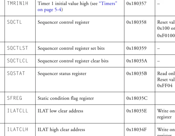
0x16 TMRIN1L Timer 1 initial value low (see “Timers” on page 5-4)
0x180356 –
0x17 TMRIN1H Timer 1 initial value high (see “Timers”
on page 5-4)
0x180357 –
0x18 SQCTL Sequencer control register 0x180358 Reset value:
0x100 or 0xF01001 0x19 SQCTLST Sequencer control register set bits 0x180359 – 0x1A SQCTLCL Sequencer control register clear bits 0x18035A –
0x1B SQSTAT Sequencer status register 0x18035B Read only,
Reset value:
0xFF04 0x1C SFREG Static condition flag register 0x18035C
0x1E ILATCLL ILAT low clear address 0x18035E Write only register 0x1F ILATCLH ILAT high clear address 0x18034F Write only
register 1 According to IRQEN strap.
Table 3-9. Sequencer Registers (Continued)
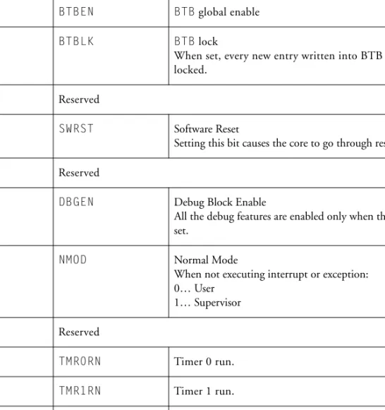
Sequencer Control Register – SQCTL
The sequencer is controlled and configured by writing to this register, which is set to 0x0100 after reset.
Table 3-10. SQCTL Register Bit Descriptions
Bit # Name Definition
0 BTBEN BTB global enable
1 BTBLK BTB lock
When set, every new entry written into BTB is locked.
4:2 Reserved
5 SWRST Software Reset
Setting this bit causes the core to go through reset.
7:6 Reserved
8 DBGEN Debug Block Enable
All the debug features are enabled only when this bit is set.
9 NMOD Normal Mode
When not executing interrupt or exception:
0… User 1… Supervisor
11:10 Reserved
12 TMR0RN Timer 0 run.
13 TMR1RN Timer 1 run.
19:16 INTERRUPT
LEVEL/EDGE
Determines if IRQ3–0 interrupt pins are level- or edge-sensitive. (0=edge, 1=level)
Sequencer Control Register Set Bits – SQCTLST
Alias for SQCTL for write: when writing to this address, the data written into this register is the OR of the register old value and the data written into it. A ‘1’ in any bit of the written data sets the corresponding bit in
SQCTL, while a ‘0’ in written data does not change the bit value.
Sequencer Control Register Clear Bits – SQCTLCL
Alias for SQCTL for write: when writing to this address, the data written into this register is the AND of the register old value and the data written into it. This way a ‘0’ in any bit of the written data clears the correspond- ing bit in SQCTL, while a ‘1’ in written data does not change the bit value.
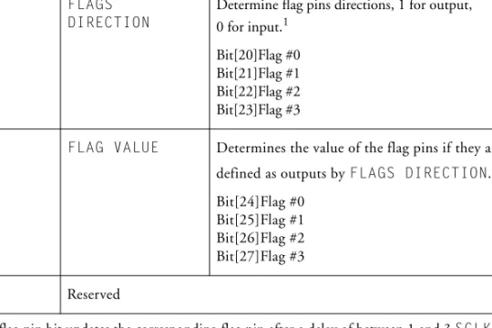
23:20 FLAGS
DIRECTION
Determine flag pins directions, 1 for output, 0 for input.1
Bit[20]Flag #0 Bit[21]Flag #1 Bit[22]Flag #2 Bit[23]Flag #3
27:24 FLAG VALUE Determines the value of the flag pins if they are defined as outputs by FLAGS DIRECTION.1 Bit[24]Flag #0
Bit[25]Flag #1 Bit[26]Flag #2 Bit[27]Flag #3
31:28 Reserved
1 The flag pin bit updates the corresponding flag pin after a delay of between 1 and 3 SCLK cycles.
Setting and clearing a flag bit might not affect the pin if both operations occur during that delay.
The recommended way to set and clear the flag pin bit is to get an external indication that the bit has been set before clearing it. Otherwise, insert (2 ⴛ LCLKRAT) instruction lines between the set and the clear to compensate for the delay.
Table 3-10. SQCTL Register Bit Descriptions (Continued)
Bit # Name Definition
Sequencer Status Register – SQSTAT
This is a read-only register that holds information about the current status of the sequencer. The initial value of this register after reset is 0xFF00. Table 3-11. SQSTAT Register Bit Descriptions
Bit # Name Definition
1:0 MODE Operation mode:
00… User 01… Supervisor 11… Emulation
2 IDLE Set when the TigerSHARC® DSP is in idle state.
7:3 SPVCMD Five LSBs of the last executed supervisor TRAP instruc- tion. This is useful for OS kernels (can hold requested BIOS functions) and SW debuggers.
11:8 EXCAUSE Exception cause of the last exception 0000… TRAP instruction
0001… Watchpoint match 0010… Floating-point exception 0011… Illegal instruction line 0100… Non-aligned access 0101… Access to protected register 0110… Performance monitor counter wrap 0111… IALU – access to illegal address 1000… Emulation exception while emulation is
disabled
1111… No exception has occurred since reset 15:12 EMCAUSE Emulation cause of the last emulation trap:
0000… EMU instruction 0001… JTAG caused emulation 0010… Watchpoint match
1111… No emulation exception has occurred since reset
19:16 FLG Flag pins value (as inputs).
SFREG Register
Static flags are used as static copies of conditions. When the programmer wishes to keep a condition value after another instruction may change its value, it can be copied into the SFREG and used later as a condition. All static condition flags are grouped into the SFREG register (see the
SF 1/0 += AND cond; SF1/0 = cond; instruction in the TigerSHARC DSP Instruction Set Specification for information about how this register is updated and used).
ILAT Registers
The ILAT register is a single 64-bit register accessed as two 32-bit registers
ILATH and ILATL. Each bit is dedicated to an interrupt. When an interrupt occurs, the corresponding bit is set. The interrupt bits order is set accord-
31:20 Reserved
Table 3-12. SFREG Register Bit Descriptions
Bit # Name Definition
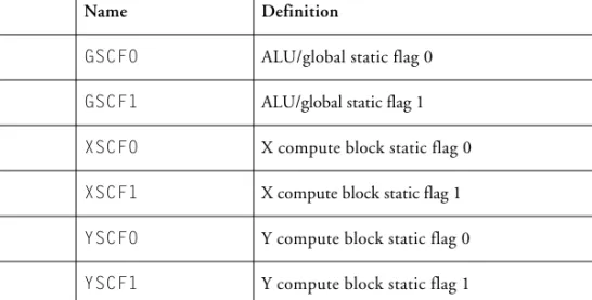
0 GSCF0 ALU/global static flag 0 1 GSCF1 ALU/global static flag 1 2 XSCF0 X compute block static flag 0 3 XSCF1 X compute block static flag 1 4 YSCF0 Y compute block static flag 0 5 YSCF1 Y compute block static flag 1
31:6 Reserved
Table 3-11. SQSTAT Register Bit Descriptions (Continued)
Bit # Name Definition
ing to the interrupt priority—bit 0 having lowest priority. The bits are shown in Table 3-13:
Table 3-13. ILAT Register Bit Descriptions
Bit # Definition
1:0 Reserved
2 Timer #0 low priority
3 Timer #1 low priority
5:4 Reserved
6 Link #0 interrupt
7 Link #1 interrupt
8 Link #2 interrupt
9 Link #3 interrupt
13:10 Reserved
14 DMA #0 interrupt
15 DMA #1 interrupt
16 DMA #2 interrupt
17 DMA #3 interrupt
21:18 Reserved
22 DMA #4 interrupt
23 DMA #5 interrupt
24 DMA #6 interrupt
25 DMA #7 interrupt
28:26 Reserved
29 DMA #8 interrupt
30 DMA #9 interrupt
31 DMA #10 interrupt
32 DMA #11 interrupt
36:33 Reserved
37 DMA #12 interrupt
38 DMA #13 interrupt
40:39 Reserved
41 IRQ0 interrupt pin 42 IRQ1 interrupt pin 43 IRQ2 interrupt pin 44 IRQ3 interrupt pin
47:45 Reserved
48 VIRPT (vector interrupt)
49 Reserved
50 Bus lock interrupt
51 Reserved
Table 3-13. ILAT Register Bit Descriptions (Continued)
Bit # Definition
Two other accesses to the ILAT registers are through the set (ILATSTL or
ILATSTH) and clear (ILATCLL or ILATCLH) addresses. Writing to the set addresses will update the ILAT register to the OR of old value and written value. As a result, every set bit in the written data will set the correspond- ing bit in the ILAT register. Writing to the clear address will AND the data written with the old data of the ILAT register. In this case, a zero bit in the input data will clear the corresponding bit in ILAT, while a set bit will keep it unchanged. The consequences and restrictions of these accesses are detailed in “ILAT Register” in Chapter 5 Interrupts.
IMASK Register
The IMASK register is a single 64-bit register accessed as two 32-bit regis- ters IMASKL and IMASKH. Mask bits[63:61, 59:0] are individually
dedicated to different interrupts in the same manner as the bit assignment in the ILAT register.
52 Timer 0 high priority
53 Timer 1 high priority
56:54 Reserved
57 Hardware Error
61:58 Reserved
62 Exception
63 Emulation debug (highest priority)
Table 3-13. ILAT Register Bit Descriptions (Continued)
Bit # Definition
The IMASK bits are as follows:
• Bits[63:61] and bits[59:0] – Interrupt enables, identical to the cor- responding bits in the ILAT register
• Bit[60]– Global enable hardware interrupts The initial value of IMASK after reset is as follows:
0x90010061E3C3C000 – normal reset
0x90011E61E3C3C000 – reset with IRQ enable strap active PMASK Register
The PMASK register is a single 64-bit register that is accessed as two 32-bit registers, PMASKL and PMASKH. The PMASK register is identical to the IMASK register in bit assignment:
• Bits[63:61] and bits[59:0] – Interrupt bits, identical to the corre- sponding bits in the ILAT register
• Bit[60]– Global disable hardware interrupts The initial value of PMASK after reset is 0x0.
Interrupt Vector Table Register Groups
The 32-bit register groups 0x38 and 0x39 are dedicated to interrupt con- trol—see Table 3-14 and “Interrupt Vector Table” on page 5-2.
Table 3-14. Interrupt Vector Table (IVT)
Group 0x38 - Reg #
Register Name Register Type Direct Mem.
Address
Reset Value
Reg #2 IVTIMER0LP Timer #0 low priority 0x180702 –
Reg #3 IVTIMER1LP Timer #1 low priority 0x180703 –
Reg #6 IVLINK0 Link #0 Reg 0x180706 –
Reg #7 IVLINK1 Link #1 Reg 0x180707 –
Reg #8 IVLINK2 Link #2 Reg 0x180708 –
Reg #9 IVLINK3 Link #3 Reg 0x180709 –
Reg #14 IVDMA0 DMA #0 Reg 0x18070E 0x0
Reg #15 IVDMA1 DMA #1 Reg 0x18070F 0x0
Reg #16 IVDMA2 DMA #2 Reg 0x180710 0x0
Reg #17 IVDMA3 DMA #3 Reg 0x180711 0x0
Reg #22 IVDMA4 DMA #4 Reg 0x180716 0x0
Reg #23 IVDMA5 DMA #5 Reg 0x180717 0x0
Reg #24 IVDMA6 DMA #6 Reg 0x180718 0x0
Reg #25 IVDMA7 DMA #7 Reg 0x180719 0x0
Reg #29 IVDMA8 DMA #8 Reg 0x18071D 0x0
Reg #30 IVDMA9 DMA #9 Reg 0x18071E 0x0
Reg #31 IVDMA10 DMA #10 Reg 0x18071F 0x0 Group 0x39 -
Reg #
Register Name Register Type Direct Mem.
Address
Reset Value
Reg #0 IVDMA11 DMA #11 Reg 0x180720 0x0
Reg #5 IVDMA12 DMA #12 Reg 0x180725 0x0
Reg #6 IVDMA13 DMA #13 Reg 0x180726 0x0
Reg #9 IVIRQ0 IRQ0 Reg pin 0x180729 0x1000 0000
Reg #10 IVIRQ1 IRQ1 Reg pin 0x18072A 0x0800 0000
Reg #11 IVIRQ2 IRQ2 Reg pin 0x18072B 0x0C0 0000
Reg #12 IVIRQ3 IRQ3 Reg pin 0x18072C 0x0
Reg #16 VIRPT VIRPT (vector Reg) 0x180730 –
Reg #18 IVBUSLK Bus Lock Vector 0x180732 –
Reg #20 IVTIMER0HP Timer 0 high priority 0x180734 –
Reg #21 IVTIMER1HP Timer 1 high priority 0x180735 –
Reg #25 IVHW Hardware Error 0x180739 –
Reg #30 IVSW Software Exception 0x18073E –
Table 3-14. Interrupt Vector Table (IVT) (Continued)
BTB Direct Access
The BTB is, in fact, a memory that is mapped as registers and is generally only accessed directly for production testing. Before accessing, the BTB must be disabled by clearing the BTBEN in the sequencer control register (SQCTL).
The following register groups are dedicated to BTB direct accesses, where nn stands for entry number:
• 0x30: BTB0TGnn BTB tags way #0 entries (nn) 0:31 (address
0x180600:0x18061F)
• 0x31: BTB1TGnnBTB tags way #1 entries (nn) 0:31 (address
0x180620:0x18063F)
• 0x32: BTB2TGnnBTB tags way #2 entries (nn) 0:31 (address
0x180640:0x18065F)
• 0x33: BTB3TGnnBTB tags way #3 entries (nn) 0:31 (address
0x180660:0x18067F)
• 0x34: BTB0TRnn BTB target way #0 entries (nn) 0:31 (address
0x180680:0x18069F)
• 0x35: BTB1TRnn BTB target way #1 entries (nn) 0:31 (address
0x1806A0:0x1806BF)
• 0x36: BTB2TRnn BTB target way #2 entries (nn) 0:31 (address
0x1806C0:0x1806DF)
• 0x37: BTB3TRnn BTB target way #3 entries (nn) 0:31 (address
0x1806E0:0x1806FF)
• 0x3B: BTBLRUnn BTB LRU all entries (nn) (address
0x180760:0x18077F)
The tag entry format is:
• Bits[1:0] – Alignment
• Bits[18:2] – Tag (address [22:6]) The target entry format is:
• Bits[0] – Jump by RTI
• Bits[1] – Jump by CJMP
• Bits[23:2] – Target address The LRU entry format is:
• Bits[2:0] – LRU entry 0
• Bits[5:3] – LRU entry 1
• Bits[8:6] – LRU entry 2
• Bits[11:9] – LRU entry 3
Debug Register Groups
The debug registers use groups 0x3D, 0x3E and 0x1B and are described in Table 3-15, “Debug Register Groups,” on page 3-31. The debug registers can only be accessed as single word.
In emulation mode the debug registers can be accessed only by move, register-to-register, or immediate data load instructions. These registers can not be loaded from or stored to memory directly.
Table 3-15. Debug Register Groups
Group 0x3D Reg #
Register Name
Register Type Direct Mem
Address
Remarks
Reg 0x00 WP0CTL Watchpoint 0 control 0x1807A0 Reset value: 0x0 Reg 0x01 WP1CTL Watchpoint 1 control 0x1807A1 Reset value: 0x0 Reg 0x02 WP2CTL Watchpoint 2 control 0x1807A2 Reset value: 0x0 Reg 0x04 WP0STAT Watchpoint 0 status 0x1807A4 Read only; reset
value: 0x0XXXX Reg 0x05 WP1STAT Watchpoint 1 status 0x1807A5 Read only; reset
value: 0x0XXXX Reg 0x06 WP2STAT Watchpoint 2 status 0x1807A6 Read only; reset
value: 0x0XXXX
Reg 0x08 WP0L Watchpoint 0 low address 0x1807A8 –
Reg 0x09 WP0H Watchpoint 0 high address 0x1807A9 –
Reg 0x0A WP1L Watchpoint 1 low address 0x1807AA –
Reg 0x0B WP1H Watchpoint 1 high address 0x1807AB –
Reg 0x0C WP2L Watchpoint 2 low address 0x1807AC –
Reg 0x0D WP2H Watchpoint 2 high address 0x1807AD –
Group 0x1B Reg #
Register Name
Register Type Direct Mem
Address
Remarks
Reg 0x00 EMUCTL Emulation control 0x180360 Reset value: 0x01
Reg 0x01 EMUSTAT Emulation status 0x180361 Read only, Reset
value: 0x0 Reg 0x03 PRFM Performance monitor mask 0x180363 Reset value: 0x0
Reg 0x04 CCNT0 Cycle counter low 0x180364 Reset value: 0x01
Reg 0x05 CCNT1 Cycle counter high 0x180365 Reset value: 0x01
Reg 0x06 PRFCNT Performance monitor counter 0x180366 Reset value: 0x0
Reg 0x08 EMUDAT Emulation data register 0x180368 -
Reg 0x0C - 0x0F
EMUIR Emulation instruction register – read only; for Sequencer fetch only
0x18036C -
0x18036F
Read only; reset value:
4 NOP inst.
Reg 0x10 TRCBMASK Trace buffer mask 0x180370 Read only; reset value:
0xFFFFFF00
Reg 0x18 TRCBPTR Trace buffer pointer 0x180378 Read only; reset value:0x0
Reg 0x1A IDCODE JTAG ID Code 0x18037A
Group 0x3e Reg #
Register Name
Register Type Direct Mem
Address
Remarks
Reg 0x0 TRCB0 Trace buffer 0 0x1807C0 Read only; reset
value: 0x0
Reg 0x1 TRCB1 Trace buffer 1 0x1807C1 Read only; reset
value: 0x0
Reg 0x2 TRCB2 Trace buffer 2 0x1807C2 Read only; reset
value: 0x0
Reg 0x3 TRCB3 Trace buffer 3 0x1807C3 Read only; reset
value: 0x0
Reg 0x4 TRCB4 Trace buffer 4 0x1807C4 Read only; reset
value: 0x0
Table 3-15. Debug Register Groups (Continued)
Emulation Status Register – EMUSTAT
Reg 0x5 TRCB5 Trace buffer 5 0x1807C5 Read only; reset
value: 0x0
Reg 0x6 TRCB6 Trace buffer 6 0x1807C6 Read only; reset
value: 0x0
Reg 0x7 TRCB7 Trace buffer 7 0x1807C7 Read only; reset
value: 0x0 1 These registers are cleared by JTAG reset pin (TRST).
Table 3-16. EMUSTAT Register Bit Descriptions
Bit # Name Definition
0 EMUMOD Indicates that the TigerSHARC® DSP is in emula- tion mode.
1 IRFREE Indicates that the EMUIR is ready for insertion of a new instruction from JTAG.
31:2 Reserved
Table 3-15. Debug Register Groups (Continued)
Emulation Control Register – EMUCTL
The debug control register is a scannable register that is cleared after JTAG reset.
IDCODE
IDCODE is a JTAG code register. The value is: <version>27811CB, where
<version> is a four-bit value indicating silicon revision.
Performance Monitor Mask – PRFM
The performance monitor identifies which of the following events is counted by the performance monitor counter (PRFCNT). Bits[30:0] indi- Table 3-17. EMUCTL Register Bit Descriptions
Bit # Name Definition
0 EMEN Emulation mode enable.
When set, the TigerSHARC® DSP can go into emula- tion mode. When clear, all causes for emulation excep- tion are ignored.
1 TEME TMS emulation exception enable.
When set, an emulation exception is issued on the TMS pin rising edge.
2 EMUOE EMU output enable.
When set, the EMU pin is driven.
3 SPFDIS When set, emulation registers, other than EMUCTL, can not be written in supervisor mode.
31:4 Reserved
cate which events are monitored and bit[31] indicates if the events in the same cycle are summed or OR’ed. The entire register is cleared after reset.
Table 3-18. PRFM Register Bit Descriptions
Bit # Name Definition
5:0 NGR Non granted requests:
Bit[0] … Sequencer (fetch) Bit[1]… JALU
Bit[2]… KALU
Bit[3]… DMA – internal bus request
Bit[4] … DMA – write from external memory to internal memory
Bit[5]… U – internal bus request (IFIFO)
11:6 GR Granted requests:
Bits[11:6] Bit[6]… Sequencer (fetch) Bit[7]… JALU
Bit[8] … KALU
Bit[9] … DMA – internal bus request
Bit[10]… DMA – write from external memory to internal memory
Bit[11]… BIU – internal bus request (IFIFO) 14:12 BUS0 Bus 01transaction types:
Bit[12]… Single word Bit[13]… Long word Bit[14]… Quad word 17:15 BUS1 Bus 11 transaction types:
Bit[15]… Single word Bit[16]… Long word Bit[17]… Quad word 20:18 BUS2 Bus 21 transaction types:
Bit[18]… Single word Bit[19]… Long word Bit[20]… Quad word
Performance Monitor Counter – PRFCNT
The purpose of the performance counter is to register the cycle at which any one of the monitored conditions occurs. The monitored condition is identified by the performance monitor mask register (PRFM). The register is cleared after reset.
Cycle Counters – CCNT0 and CCNT1
The cycle counter is 64 bits long. The two Uregs that make up the cycle counter are called CCNT0 and CCNT1. CCNT is cleared on JTAG reset. These two registers cannot be accessed with a long word access; they can only be accessed in two single accesses. They can be written in emulator or super- visor modes only, although they are readable in all modes.
25:21 MODULE Executed instructions by modules:
Bit[21]… JALU Bit[22]… KALU
Bit[23]… Compute block X Bit[24]… Compute block Y Bit[25]… Control flow instruction
26 VBT Virtual bus transactions
27 SCYCLE Stall cycles
28 BTBPR BTB predictions
29 ISL Aborted instruction lines
30 CCYCLE User clock cycles
31 SUMEN Sum enable
1 Monitoring is performed on transactions driven on bus #n (n is 0, 1 or 2), including virtual bus transactions.
Table 3-18. PRFM Register Bit Descriptions (Continued)
Bit # Name Definition
Emulation Data Register – EMUDAT
This is one of the JTAG registers. It is used for data insertion and extrac- tion in emulation mode. After reset the value of EMUDAT is undefined.
Emulation Instruction Register – EMUIR
This register is reserved for sequencer usage; any read from or write to this register by an application is illegal and may cause unpredictable results.
The sequencer fetches instructions from this register in emulation mode.
For JTAG, this is a scan register used to insert instructions for execution.
The default value after reset is a NOP instruction.
Trace Buffer – TRCB0 to TRCB7 and TRCBPTR
Every time the TigerSHARC® DSP executes a non-sequential fetch, the PC of the non-sequentially fetched instruction is written into one of the trace buffer registers. The first write is into trace buffer #0; the second to
#1, and so on in a circular manner. The trace buffer pointer (3 bits) points to the last written trace buffer.
After reset, the trace buffer registers (TRCB) and pointer (TRCBPTR) are all set to zero. All the trace buffer registers are read by software only.
For more information, see “Instruction Address Trace Buffer (TBUF)” on page 9-11.
Watchpoint Control – WP0CTL, WP1CTL and WP2CTL
Each of the three watchpoints has a control register used to define its operation.
1:0
Opmode
Reserved
7:2
31:16 15:13
W Counter
EXtype
11:10 9
BM R
8 12
WPANDWPOR/SSTP/
The register bits decode as follows:
After reset, the operating mode is IDLE (00) and the other fields of the register are undefined.
Table 3-19. WPxCTL Register Bit Descriptions
Bit # Name Definition
1:0 OPMODE Operation Mode:
00… Watchpoint disabled
01… Searching for match on address 10… Searching for match on range 11… Searching for match outside range
7:2 BM Bus Master:
Bit[2]… Sequencer (only for watchpoint 0) Bit[3]…JALU
Bit[4]…KALU
Bit[5]…DMA – internal address only Bit[6]…BIU – internal address only (IFIFO) Bit[7]…Sequencer – real transactions (in fetch stage)
8 R Refer to read transactions.
9 W Refer to write transactions.
11:10 EXTYPE On count expiration do:
00… No exception 01… Exception 10… Emulation trap 11… Reserved
12 SSTP/WPOR/
WPAND
Single step bit – in WP0CTL register only.
Watchpoint OR bit – in WP1CTL register only.
Watchpoint AND bit – in WP2CTL register only.
15:13 Reserved
31:16 COUNTER Watchpoint counter initialization.
Watchpoint Status – WP0STAT, WP1STAT and WP2STAT
Each of the three watchpoints has a status register used to indicate its operation.
After reset, the EX field is in IDLE state (00) and Value is undefined.
Watchpoint Address Pointers – WP0L, WP1L, WP2L, WP0H, WP1H and WP2H
The Watchpoint Address Pointers are 32-bit pointers defining the address, or address range, of the watchpoints. Their value after reset is undefined.
Table 3-20. WPxSTAT Register Bit Descriptions
Bit # Name Definition
15:0 VALUE Watchpoint counter current value 17:16 EX Watchpoint is executing:
00… Watchpoint disabled 01… Searching for match 11… Watchpoint count expired 31:18 Reserved
JTAG Registers
The JTAG port includes access to the following registers*.The first col- umn indicates the five bits of the IR field (IR[4:0]). For additional information, refer to “JTAG Instruction Register” on page 9-16.
* Note: LSB is the first to be shifted out through the TDO.
Table 3-21. JTAG Port Access
If IR4:0 value is... Corresponding instruction is... To...
01000 EMUIR Scan in EMUIR register
10100 EMUDAT Scan the EMUDAT register
01110 IDCODE Scan the ID code register 11110 SAMPLEPC Sample the PC from which the
TigerSHARC® DSP is running.
01001 WP0CS Scan out WP0 status, and scan in WP0 control
11001 WP0L Scan WP0 low
00101 WP0H Scan WP0 high
10101 WP1CS Scan out WP1 status, and scan in WP1 control
01101 WP1L Scan WP1 low
11101 WP1H Scan WP1 high
00011 WP2CS Scan out WP2 status, and scan in WP2 control
10011 WP2L Scan WP2 low
External Port Registers
The external port (EP) includes three units:
• Bus Control/Status registers (BIU)—requiring one register group
• DMA—requiring four register groups
• Links—requiring three register groups
01011 WP2H Scan WP2 high
00100 EMUCTL Scan EMUCTL register
01100 EMUSTAT Scan EMUSTAT register
11111 BYPASS Bypass
Table 3-22. External Port Register Groups
Group 0x24 Reg # Register Quad BIU Registers Direct Mem Address
Remarks
Reg 0x0 SYSCON1 System configuration reg- ister (see “SYSCON Pro- gramming” on page 6-12)
0x180480 Reset value:
0x279E7
Reg 0x3 BUSLK System control register 0x180483 Reset value:
0x0
Reg 0x4 SDRCON1 SDRAM configuration
register (see “SDRAM Programming” on page 6-45)
0x180484 Reset value:
0x0
Table 3-21. JTAG Port Access (Continued)
If IR4:0 value is... Corresponding instruction is... To...
Reg 0x6 SYSTAT System status register 0x180486 Read only Reg 0x7 SYSTATCL System status register
destructive address (clear error)
0x180487 Read only
Reg 0xC BMAX Maximum cycle count for
bus fairness (see “Bus Fairness—BMAX” on page 6-83)
0x18048C Reset value:
0xFFFF
Reg 0xD BMAXC Current count on BMAX 0x18048D Read only;
Reset value:
0xFFFF
Group 0x3A Reg # Register Quad AutoDMA Registers Direct Mem Address
Remarks
No access AUTODMA0 AutoDMA register 0 0x180740 -
0x180743 –
No access AUTODMA1 AutoDMA register 1 0x180744 -
0x180747 –
Group 0x20 Reg # Register Quad External port DMA TCBs
(DMA channels 0 - 3)
Direct Mem Address
Remarks
Reg 0x0 - 3 DCS0 DMA channel 0 source
TCB
0x180400-3 Reset value:
0xD300 0000 0000 0000 0100 0004 0000 0000 or 0x02, 3
Table 3-22. External Port Register Groups (Continued)