Hungarian: https://doi.org/10.2478/amt-2018-0001 https://eda.eme.ro/handle/10598/30360
Materials Science and Engineering – Some Aspects in Central and Eastern European (CEE) Countries
József GYULAI
Hungarian Academy of Sciences, Resource Centre for Energy Research, Institute of Technical Physics and Materials Science, MFA, Budapest, Hungary, gyulai.jozsef@energia.mta.hu
Abstract
This introductory paper summarizes the characteristics of how “Science” and “Engineering” differ from each other, forming the interdisciplinary topic of Materials Science and Engineering (MS&E). It will be shown how microelectronics has developed from modern materials science, causing a change in paradigm, and how microelectronics has become the “mother” science of informatics, changing life on Earth. To prove the importance of materials, a table is shown summarizing how modern MS&E forms the basis of practically all industries. The situation and development state of MS&E in CEE countries - despite different levels of indus- trialization – have some characteristics in common, and the way to development might also have techniques in common.
We will also mention the knowledge base that CEE countries possessed during the period of political change, and the likely future that an elderly scientist foresees for the region with the help of young ambitious scien- tists.
Keywords: material science, engineering, microelectronics, interdisciplinary material science.
Introduction
This paper is devoted to young engineering stu- dents with the aim of strengthening their devo- tion to a future career. Before we turn to the topic of this paper, a short chapter is included to draw attention to how the 21st century places a heavy onus on the shoulders of these future engineers.
The global success of engineering is a key factor in keeping our planet habitable. A safe solution seems to be the so-called “Circular economy”, which states that all production and consumption processes are part of a closed cycle of material flow requiring minimum energy. It is believed that there is no more important a task in scien- ce today than tstudy if, and if so how ten billion people can live on Earth without catastrophically destroying the interdependent network of living creatures. This is the message that must be clarifi- ed to young engineers.
To find the answer, a few words are devoted to the often confused relationship of “science” to
“engineering”? Scientists, especially experimen-
talists, seek and find new phenomena and try to find explanations for experimentally observed facts. In this often “curiosity driven” process, mo- dels are defined based on mathematics, informa- tion technology, etc. the level of which, of course, is dependent on the available knowledge at the time. The applications of their work in the future are not immediately foreseen. Thus, when plan- ning an experiment, numerous influencing fac- tors must be neglected in order to arrive at a solu- tion that best fits the state of theoretical develop- ment at that time. Once basic laws and facts are accepted, future talented “engineer-scientists”
look at and treat basic laws of physics, chemistry etc. as “tools” which can be used to form mate- rials into structures - products with expected, or rather with predetermined properties. Therefore, the engineer-scientist has to account for as many as possible at his time of these by constraint pa- rameters in order to arrive at a better defined solution, a solution which enables the building of reliable future products. If this definition of engineering science is accepted, then a second
step follows in which a collective of engineers will define and optimize parameters such as tempe- rature, time duration, pressure, chemical doping, etc., under which these law-based “tools” should act and change properties of the material in ques- tion. These conditions, rules and prescriptions will convert ‘experiment’ into a ‘product’, whose final acceptance will be evident in the economy.
Materials science and engineering (MS&E), in general
Modern MS@E is the daughter of informatics. It does not imply that the earlier forms of this sci- ence were not useful – think e.g. of swords of Da- mascus, or the dawn of metallurgy described in the book of Agricola, the Dē rē metallica (1556) [1].
But, quantification of metallurgical processes by the use of informatics, in a very broad sense, has caused a fundamental paradigm change. Today, the understanding of processes, often on an ato- mic scale, allows mankind to improve technology and to produce products on an industrial scale.
It may not be an exaggeration that microelectro- nics technology was and still is the leading field of science that drives automation, robotics, system control and quality management forward, by de- manding new and better solutions. A summary of a few examples follow relating to materials scien- ce and the demands of transistor technology.
In this example, the goal is - as the drawing from Figure 1 shows - to control the flight of charge carriers within a so-called space charge layer, from the source (S) region to the drain (D), (in the rear of Figure 1 under a SiO2-insulated metal layer on top, called the gate (G)). Carrier A flies freely: “ballistically accelerated”, carrier B’s track interacts with potential wells of deliberately embedded ions to control operation voltage. This interaction, however, “heats” the crystal, and this heat must be conducted away – a serious problem
if, for example. millions of transistors are connec- ted to form, e.g., a logic circuit.
“Exponential” means that the number of ele- ments doubles yearly. Moore was modest enough to think that this unprecedented development would stay with us, say, till end of the seventies.
It turned out that his modesty was an understa- tement: we are still seeing the law being fulfilled even today, though with some additional correcti- ons, e.g., the exact 2D-version of an integrated cir- cuit (IC) would not allow further miniaturization, structures must leap out into a 3rd dimension.
Nature, however, has assisted mankind by me- ans of the so-called “Dennard scaledown”: if all dimensions of a transistor are multiplied by a number smaller than one, it is only the heat emis- sion that will change and the electrical properties will remain the same. Today, industry is at “12 nm technology”, i.e. the smallest features are around 12 nm.
With this in mind, an overview can be given of what the effect of this miniaturization is upon precision of production technology, when indivi- dual transistors are smaller than a virus.
1. Defect free crystals. It is the element silicon which holds the size-record for growing a de- fect free single crystal, using the Czochrals- ki-growing technology. A few hundred kN crys- tal is sliced into 300 mm diameter crystallogra- phically oriented wafers of about 700 micron thickness, ground and polished to a few tenths of a nm root-mean-square (r.m.s.) roughness, more aptly called “smoothness”. Finally, it is cleaned beyond ‘chemical’ cleanliness, packa- ged and delivered to the semiconductor foundry.
The maximum number of surface dislocations is below 1/10 cm2.
2. Dielectric (SiO2, or high-dielectric constant) layer growth. Scaling down requires thinner and thinner insulation between the metal gate and space charge layer in the silicon. Cur- rently down to a few nm, i.e., to a thickness of few elementary cells. This thickness can grow in reduced O2-pressure in seconds, homoge- neously over the 300 mm wafer. Steps, even single atomic steps at the Si SiO2 interface, are not allowed more than at every 10,000th atom (as atomic steps involve inherently dangling chemical bonds, which can act as traps for the carriers).
3. Photolithography. To form structures with some 10 nm size requires around 100 nm wa- velength illumination in lithography. To arrive at faultless structures of a tenth of this wavel- Figure 1. Visualized tracks (ballistic, A, and scattered,
B) of charge carriers from Source (S) to Drain (D) in the so-called space charge layer of a Me- tal-Oxide-Semiconductor, MOS, transistor
ength, all diffraction must be avoided, and this requires extremely high quality optics.
4. All of the above need to be adhered to in order to perform at nearly 100% output…
It is believed that these requirements convince the Reader of the uniqueness of this industry. To add more, as sizes shrink into the nanometer ran- ge, the latest version of microelectronics is called
“nanoelectronics”, where other binary quantities, like spins, act as the carrier of digital information (“spintronics”). Then, we arrive at the next stage, quantum computing, which may reach industrial level in the coming decades. However, a decade or longer time lag is usual between successful lab experiments and mass production.
No wonder that until turn of the millennium, microelectronics merged into and fertilized all branches of industry, both physics and chemistry based ones, and we witness its slow penetration into the bioindustry. Usually the software basis of regulation first leads penetration, is followed by automatization and, finally, robotization of the hardware. Later in this paper, a summary of this fertilizing penetration of MS&E will be given.
Forms of MS&E
Two forms of MS&E are often distinguished.
One is the so-called “top down” process, the other is the “bottom up” process. The first form is the ancient idea, as it represents, e.g., the stone age technique of how sharp obsidian tools, flints were made. Analogous techniques prevail, say, in the lathe turning of metals. Here, trillions of bonds go broken resulting in heating, representing energy loss. This can be somewhat diminished using form casting. Better forms are the bottom up tech- niques, the pinnacle of which is plant life [3]. An early lecture of R. Feynman is often quoted as a prophesy of nanoscience or nanotechnology [4].
Today ground-breaking nanotechnology proces- ses use predominantly bottom-up-type processi- ng, like nanoelectronics.
Materials engineering and branches of industry
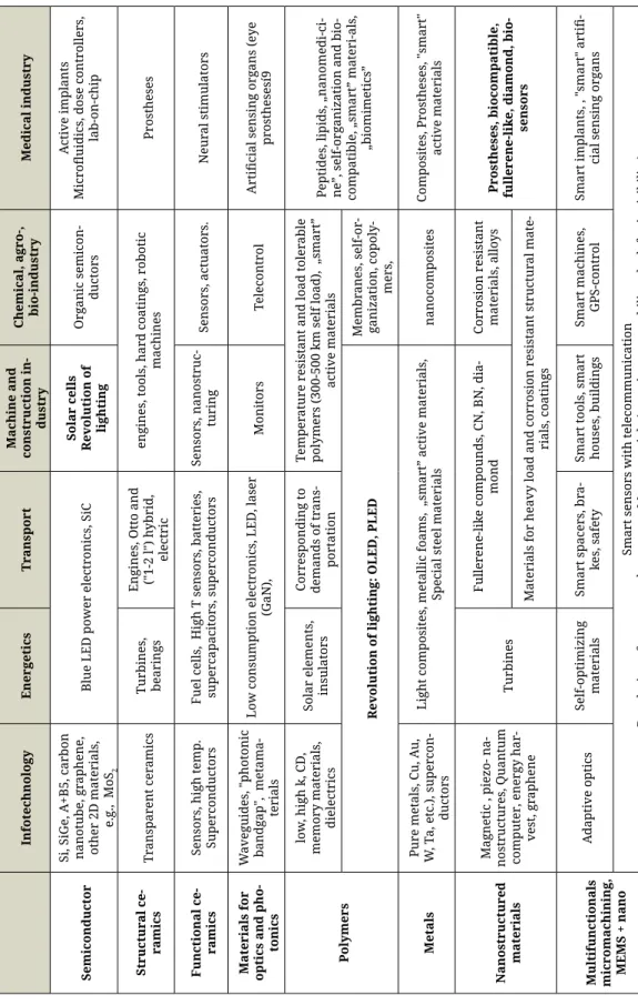
MS&E is a horizontal science: practically no pro- duct of human activity is imaginable that doesn’t involve some kind of material. It is normal that all products have a demand on a specific raw or starting material. The Table 1 summarizes to- day’s leading research in different materials and their importance in different industries. The re-
ader may find missing data, comments, but the complexity of this tutorial table must surely be convincing.
Conclusions for CEE young students, engineers
The structure of industry in CEE countries at the onset of political changes was unique. Being earlier members of an alliance, their industries were specifically developed in the interests of the military needs of the cold war, although with some consideration of local specialities. The main direction was in heavy industry (steel, oil, etc.,), thus, materials science was more like the Russi- an-Soviet “Materialovedenie”, or the GDR ”Werks- toff-Forschung” resembling more the historically important and valuable at the time of the “Old Metallurgist”. The reason? As informatics was considered by the Soviet ideology as a “capita- list pseudoscience”, modern MS&E work could start to develop ion CEEs only with the advent of fundamental political changes, the levying of em- bargo, in the nineties. This was not an easy task, as e.g., even patent matters were not considered earlier at all and a clearing-up took a lot of effort, foreign capital influx, factory shutdowns, etc.1 We had a generation of engineers, who were pre- vented from travelling, yet with huge personal experience, albeit with a kind of amateurism as seen from the outside. However, they were trai- ned in a special skill: the ability to solve problems individually, by instinct. The author’s experience in the liberated Hungary was not at all negative, though his country enjoyed a certain and relative freedom where earlier international practice was concerned.
The new freedom for the young ones in the nine- ties was difficult to live with. Scientific, industrial partnership is a matter of trust, of friendship. To build this up is not just a web partner search, but takes time and personal effort, friendly “get-toget- hers” at conferences, etc. Slowly, however, we are seeing results. Some of them are pseudo-negative, when one considers the probably never-to-return intellectual power but clever science and good industrial politics can improve this. The author’s personal exposure to the establishing of Intel in the US (1969 and thereafter) as part of his Caltech post doctorate, and his involvement in the R&D of Intel’s mother company, Fairchild Semiconduc-
1 The author’s eyes were opened in the eighties, when wor- king as a research associate at Faculty of MS&E of Cornell University (NY).
InfotechnologyEnergeticsTransportMachine and construction in- dustryChemical, agro-, bio-industryMedical industry Semiconductor Si, SiGe, A+B5, carbon nanotube, gr
aphene, other 2D materials, e.g., MoS2
Blue LED power electronics, SiCSolar cells Revolution of lightingOrganic semicon- ductors
Active implants Microfluidics, dose controllers, lab-on-chip Structural ce- ramicsTransparent ceramics
Turbines, bearings Engines, Otto and ("1-2 l") h
ybrid, electricengines, tools, hard coatings, robotic machinesProstheses Functional ce- ramics
Sensors, high temp. Superconductors Fuel cells, High T sensors, batteries, supercapacitors, superconductors
Sensors, nanostruc- turingSensors, actuators.Neural stimulators
Materials for optics and pho
- tonics
Waveguides, "photonic bandgap", metama
- terialsLow consumption electronics, LED, laser (GaN),MonitorsTelecontrolArtificial sensing organs (eye prosthesesí9 Polymers
low, high k, CD, memory materials, dielectricsSolar elements, insulators
Corresponding to demands of tr
ans- portation
Temperature resistant and load tolerable polymers (300-500 km self load), „smart” active materialsPeptides, lipids, „nanomedi-ci- ne”, self-organization and bio- compatible, „smart” materi-als, „biomimetics” Revolution of lighting: OLED, PLEDMembranes, self-or- ganization, copoly- mers, MetalsPure metals, Cu, Au, W, Ta, etc.), supercon- ductorsLight composites, metallic foams, „smart” active materials, Special steel materialsnanocompositesComposites, Prostheses, "smart" active materials Nanostructured materials
Magnetic , piezo- na-
nostructures, Quantum computer, energy har
- vest, grapheneTurbines
Fullerene-like compounds, CN, BN, dia- mondCorrosion resistant materials, alloys
Prostheses, biocompatible, fullerene-lik
e, diamond, bio- sensorsMaterials for heavy load and corrosion resistant structural mate- rials, coatings
Multifunctionals micromachining, MEMS + nano
Adaptive opticsSelf-optimizing materialsSmart spacers, bra- kes, safety
Smart tools, smart houses, buildings
Smart machines, GPS-controlSmart implants, , "smart" artifi- cial sensing organs Smart sensors with telecommunication Revolution of sensors and actuators, Metamaterials (negative permeability, cloak for invisibility);
Table 1.Interaction and expected influence of present day research in Materials Science and Engineering with different industries
tors, proves that being part of a big company, cle- ver engineers may pick up enough knowledge to start their own company. Maybe first as a compo- nent deliverer. This is what I maintain as a hope for young engineers in CEE countries. [5] [6]
References
[1] Agricola G.: De re metallica. Basel, 1556.
http://www.gutenberg.org/files/38015/38015- h/38015-h.htm
[2] Moore G.: Cramming more components onto integ- rated circuits. Electronics, 38/8. (1965).
http://archive.computerhistory.org/resources/ac- cess/text/2017/03/102770822-05-01-acc.pdf
[3] Drexler E. K.: Engines of creation: The coming era of nanotechnology. Anchor Books, New-York, 1986.
http://e-drexler.com/p/06/00/EOC_Cover.html [4] Feynman R. P.: There’s plenty of room at the bot-
tom. Előadás, American Physical Society, Caltech, Pasadena, 1959. december 29.
Átírata: http://www.zyvex.com/nanotech/feyn- man.html (letöltve: 2018. május 15.)
[5] Gyulai J.: Materials science and its importance in middle and central Europe. In: Physics and in- dustrial development. Bridging the gap. (Chand- rasekhar S. (szerk.)), Wiley Eastern Ltd., New Del- hi, 1995. 227–232.
[6] Gyulai J.: Jedlik vagy Siemens? Új Magyarország, 3.
(1993. június 26.).