2
Synthesis and mechanical characterization of wet chemically grown ZnO nanowires for nanoelectromechanical sensors
Nedves kémiai úton növesztett ZnO nanoszálak előállítása és vizsgálata nanoelektromechanikai érzékelők fejlesztése céljából
DOKTORI (PhD) ÉRTEKEZÉS Erdélyi Róbert
Pannon Egyetem - Műszaki Informatikai Kar
Molekuláris- és Nanotechnológiák Doktori Iskola vezetője: Prof. Dr. Vonderviszt Ferenc, DSc
Témavezető: Dr. Volk János, PhD
Magyar Tudományos Akadémia Természettudományi Kutatóközpont Műszaki Fizikai és Anyagtudományi Intézet
2014
DOI: 10.18136/PE.2014.558
3
Synthesis and mechanical characterization of wet chemically grown ZnO nanowires for nanoelectromechanical sensors
Értekezés doktori (PhD) fokozat elnyerése érdekében Írta:
Erdélyi Róbert
Készült a Pannon Egyetem Molekuláris- és Nanotechnológiák Doktori Iskolája keretében Témavezető: Dr. Volk János
Elfogadásra javaslom (igen / nem) ……….
(aláírás) A jelölt a doktori szigorlaton ………… % -ot ért el,
Az értekezést bírálóként elfogadásra javaslom:
Bíráló neve: ……….. ……… igen/nem
……….
(aláírás) Bíráló neve: ……….. ……… igen/nem
……….
(aláírás) Bíráló neve: ……….. ……… igen/nem
……….
(aláírás) A jelölt az értekezés nyilvános vitáján ………… % -ot ért el.
Veszprém, ……….
A Bíráló Bizottság elnöke A doktori (PhD) oklevél minősítése: ………
……….
Az EDHT elnöke
4
Table of contents
Abstract...7
Magyar nyelvű kivonat...8
Abstract (Deutsch)...9
Abbreviations...10
1. Introduction...11
1.1. Motivation...11
1.2. ZnO nanowires and nanorods as building blocks of future nanodevices...11
1.2.1. Physical properties of ZnO...11
1.2.2. Vapor-phase synthesis of ZnO nanowires and nanorods...14
1.2.3. Wet chemical growth of ZnO nanowires and nanorods...15
1.2.4. Applications of ZnO nanowires and nanorods...17
1.3. Mechanical characterization of nanowires, nanorods and nanotubes...23
1.3.1. Electrically and mechanically induced resonance analysis...24
1.3.2. Mechanical characterization via axial loading...28
1.3.3. Atomic force microscopy based methods...31
1.3.4. Other nanomechanical methods...34
1.3.5. Mechanical characterization of ZnO NWs/NRs...37
2. Methods...38
2.1. Two dimensional X-ray diffraction...38
2.2. Transmission electron microscopy...38
2.3. Field emission scanning electron microscopy...39
2.4. Focused ion beam etching...40
2.5. Electron-beam lithography...40
2.6. Nanomanipulation inside the SEM...40
2.7. Atomic force microscopy...41
2.8. Finite element method...42
5
3. Design of a novel ZnO nanowire based nanoforce sensor...44
4. Substrate effect on the growth of vertical zinc-oxide nanowires...50
4.1. Experimental subsection...52
4.2. Results and discussion...57
4.2.1. SEM and AFM study of the NWs and the different seed layers...57
4.2.2. Structural characterization of the NWs and the corresponding seed layers...60
4.2.3. Piezoelectric characterization of the NWs...64
4.2.4. The effect of seed layer annealing...65
5. Validation of the static bending test inside the SEM...69
5.1. Experimental subsection...71
5.2. Results and discussion...73
5.2.1. SEM and TEM study of the InAs nanowires...73
5.2.2. Bending modulus of wurtzite InAs nanowires...75
6. Mechanical characterization of epitaxially grown ZnO nanorods...82
6.1. Experimental subsection...82
6.2. Results and discussion...83
7. Towards the integrated nanomechanical sensor...88
7.1. Synthesis of individual vertical ZnO NWs...88
7.1.1. Experimental...89
7.1.2. Results and discussion...90
7.2. 1D mechanically gated ZnO thin film transistor...91
7.2.1. Experimental...91
7.2.2. Results and discussion...93
8. Summary...96
9. Thesis highlights.…...98
10. List of publications...100
11. Acknowledgements...102
12. Appendix...103
6
12.1. Elasticity theory of wurtzite crystals...103 12.2. Piezoelectric theory of wurtzite ZnO...104 References...106
7
Abstract
In this thesis the synthesis and mechanical characterization of wet chemically grown ZnO nanowires (NWs) as potential transducers of novel electromechanical sensors are detailed. At first the impact of various ZnO templates on their alignment and geometry was investigated.
Scanning electron microscopy, X-ray diffraction, and transmission electron microscopy revealed that the alignment, crystal structure, and geometry of the NW arrays were dictated by the crystal structure of the underlying ZnO. The mechanical properties of the individual NWs were also examined in situ inside a scanning electron microscope by a static bending test. The mean bending modulus was measured to be 32.2 GPa, which is significantly lower than that of the bulk ZnO. The validation of the bending test by the more standard resonance excitation method and the piezoelectric characterization of the NWs were also addressed.
8
Magyar nyelvű kivonat
A disszertációban a szerző egy új típusú, nanoszál alapú erőmérő megvalósítása közben elvégzett anyagtudományi, mechanikai, és méréstechnikai kutatásait mutatja be.
A leendő érzékelő olcsó és egyszerű gyártása megköveteli, hogy a ZnO nanoszálak integrálhatóak legyenek a standard félvezető technológiába, azaz azokat hagyományos hordozókon (pl. szilícium, zafír), kontrollálható geometriában ki lehessen alakítani. Ennek érdekében a szerző először a különféle ZnO magrétegek hatását vizsgálta a nedves kémiai úton növesztett ZnO nanoszálak rendezettségére és geometriájára. Atomi erőmikroszkópos, elektronmikroszkópos és röntgendiffrakciós vizsgálatok kimutatták, hogy a nanoszálak rendezettségét, kristályszerkezetét és geometriáját a magréteg kristályszerkezete határozza meg, míg a felületek érdességének észlelhető hatása nem volt. A szerző szintén kimutatta, hogy a polikristályos magrétegek hőkezelésével a nanoszálak rendezettsége nagymértékben javítható. A vezető rétegre növesztett nanoszálak piezoelektromos válaszát pásztázó tűszondás mikroszkóppal vizsgálva sikerült meghatározni a ZnO nanurudak c-tengely irányú diagonális tenzorkomponensét (d33).
A disszertációban a szerző ezután egy sok tekintetben újszerű, statikus nanomechanikai módszert hitelesít egy általánosabban elterjedt dinamikus mérési technikával, melyhez karcsú InAs nanoszálakat használ modell anyagként. Az elektronmikroszkópban végzett in situ összehasonlító vizsgálatok során az egyik manipulátor karra egy kalibrált atomi erőmikroszkópos tű, míg a másikra egy hegyes volfrám tű volt rögzítve. Előbbi lehetővé tette az egyedi nanoszálak in situ statikus hajlítgatását adott kristálytani irányban, míg utóbbival ugyanezen szálak mechanikai rezonanciájának elektromos térrel való gerjesztése történt. A szerző megmutatta, hogy a két módszer hasonló eredményre vezet. A sikeresen hitelesített hajlításos módszert ezután a szerző a mechanikai szenzorba szánt, alacsony oldalarányú ZnO nanorudak hajlítási moduluszának meghatározására használta, melynek kiértékelése során a szálak hossztengely menti keresztmetszetének inhomogenitását egy két részből felépülő mechanikai modellel vette figyelembe. A hajlítási modulusz (32.2 GPa) a tömbi ZnO Young- moduluszánál jóval kisebb értéknek adódott (140 GPa a [0001] irányban).
Végezetül a szerző egy 1 dimenziós mechanikus úton vezérelt vékonyréteg tranzisztort állított elő, amelynek elektromechanikai tesztelése során megmutatta, hogy a nedves kémiai úton növesztett ZnO nanoszálak alapját képezhetik egy nanoelektromechanikai érzékelőnek.
9
Abstract (Deutsch)
Synthese und mechanische Charakterisierung von durch nass-chemisches Verfahren gewachsenen Nanodrähten für nanoelektromechanische Sensoren
In dieser Abhandlung werden die Synthese und die mechanische Charakterisierung von durch nass-chemisches Verfahren gewachsenen ZnO Nanodrähten als potentielle Transducers von neuartigen elektromechanischen Sensoren behandelt. Durch Rasterelektronenmikroskopie, Röntgendiffraktion und Transmissionselektronenmikroskopie wurde erwiesen, dass die Anordnung, die Kristallstruktur und die Geometrie der Nanodrähte durch die Kristallstruktur des darunter liegenden ZnO Templates bestimmt wurden. Die mechanischen Eigenschaften der einzelnen Nanodrähte wurden auch in situ im Rasterelektronenmikroskop durch einen statischen Biegungstest untersucht. Der durchschnittliche Youngscher Modul bei Biegung beträgt 32.2 GPa.
Die Validierung des Biegungstests durch die standardisierte Resonanzanregungsmethode und die piezoelektrische Charakterisierung der Nanodrähten wurden auch behandelt.
10
Abbreviations:
AFM: atomic force microscope ALD: atomic layer deposition BF: bright-field
BM: bending modulus
CMOS: Complementary Metal–Oxide–Semiconductor CVD: chemical vapor deposition
DF: dark-field
DLC: diamond-like carbon DSSC: dye-sensitized solar cell FEM: finite element method
FE-SEM: field emission scanning electron microscope FIB: focused ion beam
FWHM: full width at half maximum HMT: hexamethylenetetramine
HRTEM: high-resolution transmission electron microscopy LED: light emitting diode
LF: lateral force
MBE: molecular beam epitaxy
MEMS: microelectromechanical systems
MOCVD: metal-organic chemical vapor deposition NEMS: nanoelectromechanical systems
NF: normal force
NR: nanorod
NT: nanotube
NW: nanowire
PCCW: precursor concentration controlling window PFM: piezoresponse force microscopy
PLD: pulsed laser deposition PMMA: poly(methyl methacrylate) PoC: proof-of-concept
PSPD: position sensitive photo detector RMS: root mean square
SAED: selected area electron diffraction SEM: scanning electron microscope TEM: transmission electron microscope TRCC: truncated right circular cone TRHC: truncated right hexagonal cone UV: ultraviolet
VLS: vapor-liquid-solid
VS: vapor-solid
XRD: X-ray diffraction
11
1. Introduction
1.1. Motivation
The challenges of building ZnO nanowire (NW) based NEMS (nanoelectromechanical systems) devices can be addressed on the following fronts: integration of the NWs into silicon technology; mechanical characterization in the nano-range with high confidence; electrical and electromechanical exploration; design and realization of the integrated device;
characterization of the device performance. This thesis contributes mainly to the first two goals, through the following studies:
– Investigating into the impact of the template layer on ZnO NW arrays made using low temperature wet chemical growth.
– Comparison of two independent existing in situ methods in scanning electron microscope (SEM) for the exploration of the elastic properties of one dimensional nanostructures; examination of epitaxial ZnO NWs in this manner.
In the introductory sections the basic physical properties of ZnO, and the fabrication routes and importance of ZnO NWs and nanorods (NRs) will be presented. The relevant existing experimental investigation methods of the mechanical properties of NWs, NRs, and nanotubes (NTs) will be also addressed. Then, after a short overview of the applied experimental techniques (see chapter 2), I propose the design of a novel vertical ZnO NR based integrated nanoforce sensor (see chapter 3) and my contributions to the development of such an integrated NEMS device will be described (see chapters 4, 5, 6, and 7).
1.2. ZnO nanowires and nanorods as building blocks of future nanodevices
1.2.1. Physical properties of ZnO
ZnO is a II-VI compound semiconductor. Under different growth conditions ZnO can crystallize into three structures: wurtzite, zinc blende, and rocksalt. Under ambient conditions the thermodynamically most stable phase is wurtzite, which is composed of two interpenetrating hexagonal close packed (hcp) sublattices (Fig. 1a) [1]. The measured lattice
12
parameters of the hexagonal wurtzite ZnO are a = 3.249 Å and c = 5.206 Å. It belongs to the space group of in the Schönflies notation [2]. Both Zn and O atoms are tetrahedrally coordinated to each other giving rise to polar asymmetry along the c-axis.
Figure 1. Atomic lattice of ZnO wurtzite crystal showing the tetrahedral coordination of the Zn and O atoms (a) (image a adapted from [3]). Calculated electronic band structure of wurtzite ZnO using the hybrid functional method (b) (image b adapted from [4]).
This polar nature results in many interesting properties, such as piezoelectricity, spontaneous polarization, crystal growth, polarity dependent chemical stability, and defect generation. The Zn terminated (0001) and O terminated (000 ) faces are polar in nature, while the (11 0) and (10 0) are nonpolar. In other words piezoelectricity is the result of the lack of centrosymmetry. Piezoelectric crystals produce an electric polarization in response to mechanical deformation as described in the Appendix (see subsection 12.2.). The piezoelectric tensor elements of ZnO are comparable to those of other wurtzite type materials, such as AlN, GaN, and InN (Table 1.).
Table 1. Comparison of bulk piezoelectric moduli of different wurtzite type materials (C/m2) (data are from [5]).
The electronic band structure of wurtzite ZnO can be determined by theoretical calculations using, for instance, hybrid functional method (HFM) [4]. It can be seen in Fig. 1b that both the valence band maxima and the conduction band minima occur at the Γ point k = 0
material e
33e
31e
15ZnO 0.89 -0.51 -0.45 AlN 1.46 -0.60 -0.48 GaN 0.73 -0.49 -0.3
InN 0.97 -0.57
13
indicating that ZnO is a direct band gap semiconductor. The band gap of ZnO is 3.44 eV at 0 K and 3.37 eV at room temperature [4], therefore it can be considered as a wide band gap semiconductor. The electronic band structure was determined experimentally by Ivanov et al.
using electron energy loss spectroscopy (EELS) and ultraviolet photoelectron spectroscopy (UPS) for wurtzite ZnO [6]. It turned out that the Zn face possesses more covalent character, arising from the Zn 4s – O 2p states, while the O face is more ionic.
Defect chemistry plays a very important role in controlling the electrical transport properties of ZnO [4]. Naturally, unintentionally doped ZnO shows n-type conduction with an electron concentration of about 1016–1017 cm-3 [7], however, the origin of this n-type conductivity has not been completely understood. Earlier it was believed that the n-type conduction originates due to native defects such as oxygen vacancies (Ov) and zinc interstitials (Zni). Look et al. [8]
suggested that Zni are the dominant shallow donors, rather than Ov, with an ionization energy of about 30–50 meV. However, first-principle calculations show that both Ov and Zni have high formation energies in n-type ZnO, and therefore none of these native defects are shallow donors [9]. Van de Walle [10] has theoretically shown that H is likely to be the dominant background shallow donor in ZnO materials that are exposed to H during growth. Since the H mobility is large, it can easily diffuse into ZnO in any kind of growth technique. A recent theoretical calculation of Kim and Park [11] suggests that the Coulombic attraction between Ov and Zni acts as shallow donors in ZnO. Intentional n-type doping is relatively well established through the substitution of group III elements (Al, Ga, In) on the Zn sites or group VII elements (Cl, Br, I) on the O sites [1] enabling the use of ZnO as a transparent conductive oxide (TCO) material. Park et al. e.g. demonstrated Ga doped ZnO (GZO) films showing a low electrical resistivity of 8.12·10−5 Ωcm [12].
ZnO shows strong doping asymmetry (unipolarity), i.e. doping of n-type carriers into the lattice is easy, however, similarly to most wide band gap semiconductors such as GaN, ZnS, SiC, and ZnSe p-type doping is rather challenging [13]. The problem of p-type doping in ZnO can arise for several reasons such as (i) acceptor dopants may be compensated by the native donors (Ov and Zni) and background H impurities, (ii) low solubility of the acceptor dopant impurities, and (iii) high activation energy of acceptors (deep impurity level) [14]. The possible p-type dopants in ZnO are group IA and IB elements (Li, Na, K, Ag, and Cu), group V elements (N, P, Sb, and As), and Zn vacancies (Znv) [15-17]. It has been also demonstrated experimentally that the band gap of ZnO can be tuned from 2.1 to 6.0 eV by developing CdxZn1-xO and MgyZn1-yO alloys [1]. ZnO is a promising material for optical and
14
optoelectronic applications as well, due to its wide and direct band gap, high exciton binding energy (60 meV), and ability to efficient radiative recombination [1].
ZnO in nanostructured form can be easily synthesized by physical methods at high temperature and by chemical methods at low temperature as well. Beside the above attracting physical properties, the economic, even wafer scale fabrication of ZnO nanostructures makes them promising candidates as building blocks for novel nanosized devices. Quasi-one- dimensional ZnO nanostructures (i.e. NWs, NRs, whiskers) are especially important from this aspect. In the literature terms „nanowire‟ and „nanorod‟ are usually applied as synonyms, or the ones with lower aspect ratio are frequently referred to as „nanorods‟, however there is no general consensus. In this thesis both denominations are applied. The existing growth methods can be grouped into two categories: vapor-phase synthesis and solution-phase growth.
1.2.2. Vapor-phase synthesis of ZnO nanowires and nanorods
In vapor-phase synthesis a condensed or powder source material is vaporized at elevated temperature, and then the resultant vapor phase condenses at certain conditions (temperature, pressure, atmosphere, substrate, etc.) to form the NWs with desired morphology. In order to control the diameter, aspect ratio, and crystallinity, a number of different deposition techniques can be applied including chemical vapor deposition (CVD), direct thermal evaporation, pulsed laser deposition (PLD), metal–organic chemical vapor deposition (MOCVD), etc. [18]. Growth can take place in two mechanisms. The vapor-liquid-solid (VLS) mechanism starts with the dissolution of gaseous reactants into nanosized liquid droplets of a catalyst metal, and followed by nucleation and growth of single-crystalline rods and then wires. The one dimensional growth is induced and dictated by the liquid droplets, whose sizes remain essentially unchanged during the entire process of wire growth (Fig. 2a).
Each liquid droplet serves as a virtual template to strictly limit the lateral growth of an individual wire [19]. In vapor-solid mechanism (VS) source materials are vaporized under high temperature condition and then directly condensed on the substrate placed in the low temperature region. Once the condensation process takes place, the initially condensed molecules form seed crystals serving as the nucleation sites. As a result, they facilitate directional growth to minimize the surface energy [20].
15
Fig. 2b shows SEM image of an array of vertical ZnO NWs grown by the VLS mechanism using Au particles as catalyst. The epitaxial growth on the c-Al2O3 substrate yields well- aligned distribution. The transmission electron microscopy (TEM) image of the NWs with the gold catalyst at their tips is shown in Fig. 2c [21].
Figure 2. Kinetic steps in VLS mechanism (a): (1) mass transport in the gas phase; (2) chemical reaction on the vapor–liquid interface; (3) diffusion in the liquid phase; and (4) incorporation of atoms in a crystal lattice (image a adapted from [22]). SEM micrograph of vertical ZnO NWs grown on c-Al2O3 substrate by the VLS mechanism using Au particles as catalyst (b). The epitaxial growth on c-Al2O3 yields well-aligned distribution. TEM image of the NWs with Au catalyst at their tips (c). Inset is an electron diffraction pattern recorded from a NW (images b-c adapted from [21]).
1.2.3. Wet chemical growth of ZnO nanowires and nanorods
Usually the gas-phase synthesis methods are expensive and their up-scaling is challenging. In the solution-phase synthesis, the growth process is carried out in a liquid. In most cases aqueous solutions are used and the process is referred to as wet chemical growth process. The wet chemical process of growing ZnO nanostructures has gained immense popularity due to its simplicity and tolerable growth conditions. As synthesis is carried out in aqueous solution, the growth temperatures are lower than the boiling point of water. The wet chemical growth of ZnO nanostructures was first reported by Vergés et al. [23]. However, it did not gain much interest till Vayssieres et al. [24-25] successfully used the method for the controlled fabrication of ZnO NWs on glass and Si substrates by the thermal decomposition of hexamethylenetetramine ((CH2)6N4) (HMT) and zinc nitrate (Zn(NO3)2). To initiate the growth from the substrate, a thin layer of ZnO nanoparticles was grown on the substrate (Fig.
3). Note that without any ZnO seed the growth can be hardly initiated. As a counterexample, Yuan et al. produced wet chemically grown ZnO NW arrays through heteroepitaxial growth on patterned GaN substrates due to the small lattice mismatch between the GaN substrate plane and the ZnO plane [26]. HMT is a highly water soluble, non-ionic tetradentate cyclic
16
tertiary amine. Thermal degradation of HMT releases hydroxyl ions which react with Zn2+
ions to form ZnO [27]. The ZnO deposition process undergoes by forwarding the intermediate reactions (1)-(6) in equilibrium, which helps to realize stationary growth [28].
Zn(NO
3)
2·6H
2O → Zn
2++ 2[NO
3]ˉ + 6H
2O
(1)(CH
2)
6N
4+ 6H
2O ↔ 4NH
3+ 6HCHO
(2)NH
3+ H
2O ↔ NH
4+
+ OHˉ
(3)Zn
2++ 4NH
3↔ [Zn(NH
3)
4]
2+ (4)Zn
2++ 2OHˉ ↔ solid Zn(OH)
2 (5)solid Zn(OH)
2↔ solid ZnO + H
2O
(6) Here, NH3 plays roles as weak base (pH buffer: pH =10.5) in Eq. (3) and [Zn2+] buffer in Eq.(4). Since single zinc nitrate hexahydrate molecule yields single zinc ion in Eq. (1) and single HMT molecule in weak base yields 4 hydroxide ion in Eq. (2), ZnO NR grows in [Zn2+] <
[OH-] condition and is controlled by [Zn2+]. It is a general acceptance that the role of HMT is to supply the hydroxyl ions to drive the precipitation reaction [29]. The formation of NRs rather than thin films is due to the different surface energies of different planes in the case of wurtzite ZnO. The surface formation energy of (0001) plane is the highest while that of {10 } is the lowest [30]. Therefore ZnO has a tendency to minimize the area of the (0001) plane for minimized total surface energy.
Figure 3. SEM image showing an array of ZnO NRs grown by the aqueous chemical method onto a ZnO nanostructured thin film (image adapted from [25]).
17
In this thesis the wet chemical approach was applied for ordered growth of vertical ZnO NWs, since the method has several advantages such as, low cost, low temperature, simple, and provides high yield on ZnO coated substrates.
1.2.4. Applications of ZnO nanowires and nanorods
In the last decade, ZnO NWs and NRs have been receiving a great deal of interest due to their unique properties for electronic and optoelectronic applications. A variety of ZnO NW based devices have been demonstrated, including field effect transistors, nanogenerators, ultraviolet (UV) lasers, light emitting diodes (LEDs), solar cells, and photodetectors. This section is the review of the above applications. The most productive research group in this field is leaded by Prof. Zhong Lin Wang at the Georgia Institute of Technology in Atlanta.
Gao et al. have applied the perturbation theory for calculating the piezoelectric potential distribution in an anchored vertical ZnO NW as pushed by a lateral force at the top [31]. The analytical solution produced a result that showed very good agreement with the full numerically calculated result using the finite element method (FEM). The calculations show that the piezoelectric potential in the NW almost does not depend on the z-coordinate along the NW unless very close to the two ends. The potential difference occurs between the tensed and compressed sides of the bent piezoelectric NW (Fig. 4a-b). For moderate deflection the maximum potential at the surface of the NW is directly proportional to the lateral displacement of the NW and inversely proportional to the cube of its length-to-diameter aspect ratio. The magnitude of piezoelectric potential for a NW of diameter 50 nm and length 600 nm is ~0.3 V. This potential drop across the NW serves as the gate voltage for the piezoelectric field effect transistor demonstrated by Wang et al. [32]. They demonstrated the principle of NW-based nanoforce and nanopressure sensors by building a piezoelectric field effect transistor that is composed of a ZnO NW bridging across two contacts, in which the source to drain current is controlled by the bending of the NW (Fig. 4c-h). The origin of the operation was attributed to the carrier trapping effect (Fig. 4i) and the creation of a charge depletion zone (Fig. 4j) under elastic deformation due to the coupled piezoelectric and semiconducting dual properties of ZnO. They excluded the role of piezoresistivity because of the nearly antisymmetric distribution of the strain across the width of the NW.
18
Figure 4. Side (a) and top (b) cross-section of the potential distribution for a ZnO NW with a diameter of 50 nm and a length of 600 nm at a lateral bending force of 80 nN as the result of finite element calculation (images a-b adapted from [31]). SEM images with the same magnification showing the gradual bending of a ZnO NW bridging across two contacts (c-g) and the corresponding I-V characteristics of the ZnO NW for the five different bending cases (h). Schematic of the carrier trapping effect (i) and the creation of a charge depletion zone in the NW (j) as the result of the coupled piezoelectric and semiconducting dual properties of ZnO (images c-j adapted from [32]).
The word „piezotronics‟ was created by Z. L. Wang from words piezoelectric and electronics.
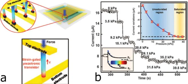
Piezotronic devices are using the piezoelectric potential created in materials with piezoelectricity as a gate to tune the charge carrier transport properties. An assembled piezotronic device for instance was reported recently by Wu et al. [33]. They demonstrated large-array three-dimensional circuitry integration of piezotronic transistors based on bundles of wet chemically grown vertical ZnO NWs. The NW bundles serve as pixels of an addressable pressure/force sensor matrix for tactile imaging. The schematic of the device is shown in Fig. 5a. At the bottom and top ends of the NWs metal-semiconductor interfaces are formed by gold contacts leading to Schottky junctions. The origin of the operation of the tactile pixels is the following. During operation the contact between the NWs and top electrodes is reverse biased. Upon applying a normal stress accumulation of piezoelectric charges at both Schottky contacts induces the distribution of piezopotential. Because of the
19
orientation of the polar c-axis in the as-synthesized ZnO NWs (red arrow in Fig. 5a), negative piezopotential is induced at the reverse-biased top Schottky contact, which raises the barrier height (Fig. 5b inset) at that contact and hence decreases the transport conductance of the device. Fig. 5b shows the current responses for an individual pixel under different pressures, illustrating the gate modulation effect of applied pressure. In other words the operation is based on barrier-interface modulation that enables enhanced sensitivity. The transistors are independently addressable and the device matrix can achieve shape-adaptive tactile imaging and self-powered, multidimensional active sensing. The 3D piezotronic transistor array has plenty of potential applications in human-electronics interfacing, smart skin, and microelectromechanical systems (MEMS). The weak point of the device is its dimensions.
The area of one NW bundle (20µm x 20µm) and the spacing between them (~100 µm) are far above the submicron range.
Figure 5. Schematic illustration of the three-dimensional tactile sensor composed of strain-gated piezotronic transistors (a), current responses for an individual pixel under different pressures (b), and schematic band diagram illustrating the change in Schottky barrier height of the reverse-biased top contact due to the modulation effect of strain-induced piezopotential (b inset) (images a-b adapted from [33]).
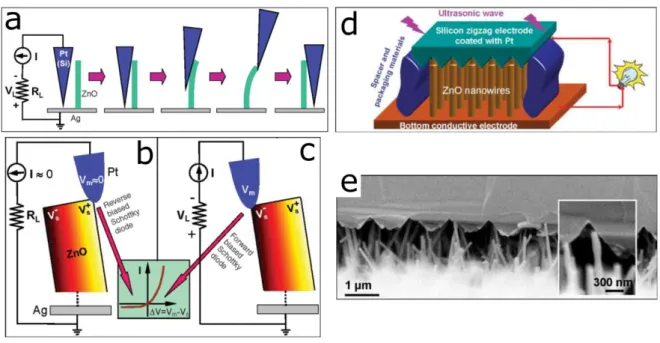
Wang et al. have converted nanoscale mechanical energy into electrical energy by means of ZnO NW arrays deflected with a conductive Pt coated atomic force microscopy (AFM) tip in contact mode [34]. The origin of the operation was attributed to the coupling of piezoelectric and semiconducting properties in ZnO. As it was shown above, the bending of a NW creates a strain field and an electric potential is created by the relative displacement of the Zn2+ cations with respect to the O2– anions, as a result of the piezoelectric effect in the wurtzite crystal structure. Thus, these ionic charges cannot freely move and cannot recombine without
20
releasing the strain, i.e. the potential difference is maintained as long as the deformation is in place and no foreign free charges are injected. The compressed side of the ZnO NW has negative potential and the stretched side has positive potential. Since ZnO is an n-type semiconductor the Pt-ZnO contact between the probe and the NW is a Schottky barrier and dominates the entire transport process. The base of the NW was grounded and an external load of RL was applied, which is much larger than the resistance RI of the NW (Fig. 6a). The AFM was scanning across the NW arrays in contact mode. When the AFM conductive tip reaches and bends the NW, it induces the deformation. Hence it is in contact with the stretched surface of positive potential so the metal–semiconductor interface in this case is a reverse-biased Schottky diode, and little current flows (Fig. 6b). When the AFM tip is in contact with the compressed side, the tip–ZnO interface is a positively biased Schottky diode, and it produces a sudden increase in the output electric current (Fig. 6c). The flow of the free electrons from the loop through the NW to the tip will neutralize the ionic charges distributed in the volume of the NW. This approach having the potential of converting mechanical energy into electricity was called "nanogenerator".
Figure 6. Experimental setup and procedures for generating electricity by deforming a ZnO NW with a conductive AFM tip (a). Schematic of the contacts between the AFM tip and the semiconductor ZnO NW at two reversed local contact potentials (b and c), showing reverse- and forward biased Schottky rectifying behavior, respectively (images a-c adapted from [34]). Schematic of the design and structure of the assembled nanogenerator (d). Cross-sectional SEM image of the nanogenerator, which is composed of aligned NWs and the zigzag electrode (e) (images d-e adapted from [35]).
21
One year later they demonstrated an assembled device including the vertically aligned NW arrays and a zigzag metal electrode placed above the NWs with a small gap [35] (Fig. 6d-e).
The zigzag electrode acts as an array of parallel integrated metal tips that simultaneously and continuously create, collect, and output electricity from all of the NWs. The device is driven by an ultrasonic wave and produces continuous direct-current output. The approach offers the technology for harvesting energy from the environment, and a potential solution for powering nanodevices and nanosystems.
However, Alexe et al. soon published a skeptical paper doubting the signal generation mechanism of the nanogenerator, since they have observed similar voltage signals and similar
"energy harvesting" from piezoelectric ZnO and nonpiezoelectric Si NW arrays [36]. Among other things they state, that the charge generated in ZnO by the piezoelectric effect will be screened by internal free charges in a very short time. They attributed the measured signals to different sources than the piezoelectric effect, such as features of the measuring instruments and set-up, therefore the energy is rather harvested from the instruments than from the NWs.
The operation principle of this vibrating top contact type nanogenerator is still under debate.
Huang et al. demonstrated room-temperature UV lasing in vertical <0001> oriented ZnO NW arrays grown on sapphire substrates [37]. The NWs formed natural laser cavities with diameters varying from 20 to 150 nanometers and lengths up to 10 micrometers (Fig. 7a-b).
They observed surface-emitting lasing action at 385 nanometers under optical excitation, with an emission linewidth less than 0.3 nanometer. The chemical flexibility and the one- dimensionality of the NWs make them ideal miniaturized laser light sources.
22
Figure 7. Tilted-view (a) and top-view (b) SEM micrographs of ZnO NWs on sapphire substrate forming natural laser cavities (images a-b adapted from [37]). Design overview of the LED based on ZnO NWs arranged in a controlled pattern on the p-GaN film (c) (image c adapted from [38]). Oriented ZnO NWs replacing the traditional nanoparticle film in a DSSC (d) and the schematic diagram of the cell in which light is incident through the bottom electrode (e) (images d-e adapted from [39]).
Zhang et al. demonstrated high-brightness UV–blue electroluminescence from n-ZnO/p-GaN (NWs/film) heterojunction LED devices [40]. They observed a blue shift in the electroluminescence with the increase of bias voltage, indicating the modification of external voltage to the band profile in the depletion region. In addition, the heterojunction LED device exhibited a high sensitivity in responding to UV irradiation. However, the position of these nanosized light sources was not controlled. Xu et al. fabricated nanoscale light emitters in the same way but in a controlled pattern on the substrate [38] (Fig. 7c).
Law et al. introduced a novel dye-sensitized solar cell (DSSC) in which the traditional nanoparticle film is replaced by a dense array of oriented, crystalline ZnO NWs (Fig. 7d) [39].
Central to this device is a thick film of NWs that provides a large surface area for the adsorption of light-harvesting molecules and direct electrical pathways to ensure the rapid collection of carriers generated throughout the device (Fig. 7e). The ZnO NW anode featured a surface area up to one-fifth as large as a nanoparticle cell. They demonstrated a full Sun efficiency of 1.5%.
Kind et al. demonstrated an optical gating phenomenon analogous to the commonly used electrical gating in ZnO NWs [41]. To characterize their photoconducting properties they
23
electrically contacted individual NWs following two different routes. The NWs were dispersed directly on pre-fabricated gold electrodes, and electron-beam lithography was used to fabricate Au electrodes on top of the NWs as well. The conductivity of the ZnO NWs proved to be extremely sensitive to UV light exposure, as shown on Fig. 8. Therefore these NWs have become promising candidates for applications such as highly sensitive UV light detectors, chemical and biological sensors, and switching devices for nanoscale optoelectronics. Yang et al. demonstrated the coupling of piezoelectric, optical, and semiconducting properties of ZnO NWs by fabricating a metal-semiconductor-metal photodetector [42]. During testing the device they applied axial compressive or tensile strain in the wire. The responsivity of the photodetector was enhanced upon UV light illumination onto the wire by introducing a –0.36% compressive strain in the wire, which effectively tuned the Schottky barrier height at the contact by the produced local piezopotential. Three-way coupling of semiconducting, photonic and piezoelectric properties of semiconductor NWs (i.e.
piezo-phototronics) offers the possibility to tune and control the electro-optical processes by strain induced piezopotential.
Figure 8. I-V curves showing dark current and photocurrent of a single ZnO NW under 365 nm, 0.3 mWcm-2 UV light illumination. The inset reveals a SEM micrograph of a 60 nm ZnO NW bridging four Au electrodes (image adapted from [41]).
1.3. Mechanical characterization of nanowires, nanorods and nanotubes
Mechanical characterization in the nanorange is highly challenging and often requires long and complicated sample preparation. Several techniques were developed by a number of
24
groups for measuring the elastic modulus and/or the strength of individual one dimensional nanostructures. Existing NW/NR/NT mechanical characterization techniques in the literature can be grouped into the following categories.
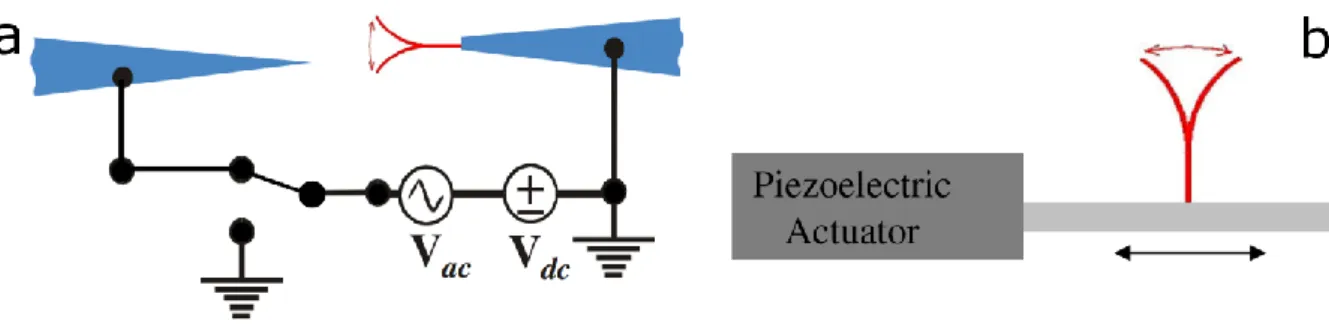
1.3.1. Electrically and mechanically induced resonance analysis
The oscillation of one-end-affixed NWs/NRs/NTs can be induced by an alternating electric field (Fig. 9a) or by periodic mechanical excitation (Fig. 9b) as well. These kinds of experiments aim to determine the natural resonance frequency, which can be related to mechanical properties. The weak point of this method is that it is limited to the elastic properties of the nanostructures, i.e. deformation, defect initiation mechanisms, and fracture/tensile strength cannot be determined. The experiments are usually carried out in SEM or TEM. Although the size of specimen stage in TEM is very limited, it has the advantage that the crystal quality of the examined nanostructures can be simultaneously observed. On the other hand, in SEM the experiments are rather comfortable due to larger specimen stage.
Figure 9. Oscillation of one-end-affixed NW induced by an alternating electric field (a) and a piezoelectric actuator (b).
Let us assume, that the natural resonance frequency of the NW is . In the case of electric- field-induced resonance (Fig. 9a) the NW as a cantilever is attached one end to an electrode and the other end is left free. The NW is then driven to vibrate by an electric field between the substrate electrode and a second electrode (counter electrode) positioned near the NW. The electric field contains both direct and alternating components with tunable frequency. The sum of the applied potential and the contact potential (VCPD) between the counter electrode and the NW can be described by the following form:
, (7)
25
where VDC is the direct part, and VAC is the alternating part of the applied electric field having a frequency of ν. The electrostatic force exerted on the NW is essentially entirely at the tip, where the charges are concentrated (as expected from classical electrostatics applied to conducting needle-shaped conductors). The force equals the product of the induced electric charge (proportional to V) and the electric field (also proportional to V). Hence the charge on the tip and the electric field can be assumed to be and , respectively. is a NW dependent constant that depends on the geometry. Therefore the electrostatic force at the tip is
=
.
(8)The relative position of the NW to the counter electrode can usually be precisely tuned using piezoelectric manipulators. As long as the equilibrium position of the NW is perpendicular to the electrostatic force (off axis position), the vibrational response of the NW as a function of the driving frequency (ν) closely follows the classical behavior predicted by the Euler- Bernoulli model for elastic rods. The appearance of resonances is classically dictated by the Euler equation
,
(9)where U(x,t) is the time dependent deflection from the equilibrium axis at position x along the NW, E is the Young‟s modulus, ρA is the mass per unit length, I is the second moment of inertia, and f(x,t) is the externally applied force. If the applied frequency matches the natural resonance frequency of the NW, resonance occurs. This is the case of forced resonance. Note that the first and the second harmonic of F(t) could both drive the NW to resonate independently (Eq. 8), therefore and are two possible resonant frequencies [43].
If the longitudinal axis of the non-excited NW is parallel to the electrostatic force (in axis position) parametric resonances can be induced due to the instability leading to oscillations at possible frequencies of [43]. However, Shi et al. have shown experimentally and theoretically that in the case of sinusoidal wave excitation only the first two parametric resonances can be found [43]. For a randomly oriented NW the vibration becomes complicated because both the transverse and the axial forces are effective, and hence
26
forced and parametric resonances would be mixed [43]. Nevertheless, one chooses whatever arrangement, it has to be ensured that the natural frequency of the NW is not overestimated as twice the true value or underestimated as half the true value by sweeping a wide frequency range.
The method was first applied by Poncharal et al. [44] in order to characterize the mechanical properties of multiwalled carbon NTs. The NTs were resonantly excited at the fundamental frequency and higher harmonics as well in a TEM (Fig. 10a-c). The relationship between these frequencies and the elastic bending modulus (BM) (i.e. the Young‟s modulus measured by bending) of the NT can be described by the following equation resulting from the Euler- Bernoulli analysis [44]
, (10)
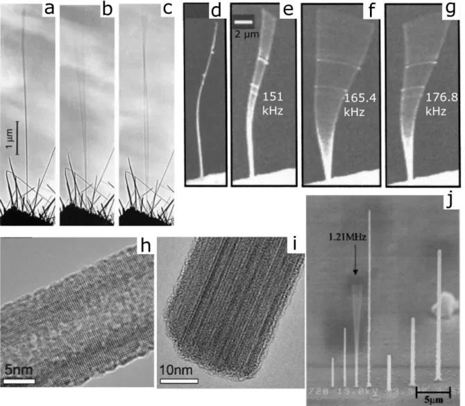
where L is the length, D is the outer diameter, Di is the inner diameter, Eb is the BM, ρ is the density, and βj is a constant for the j th harmonic: β1 = 1.875, β2 = 4.694. They found, that the elastic BM as a function of diameter decreases sharply from about 1 to 0.1 TPa with increasing diameter from 8 to 40 nm. The method has been also applied to a nanobalance for nanoscopic particles in the picogram-to-femtogram mass range. Eq. (10) is widely applied for the evaluation of such resonance experiments, however, in the case of solid NWs the equation becomes simpler due to the disappearance of the inner diameter (Di). It can be easily admitted, that the BM theoretically equals to the Young‟s modulus along the longitudinal axis of the NW: during bending the inner part of the NW suffers longitudinal compression while the outer part suffers longitudinal tension. Liu et al. [45] applied the electric-field-induced resonance technique to probe the mechanical properties of WO3 NWs directly grown on tungsten tips inside TEM. The results indicated that the BM is basically constant at diameter larger than 30 nm, while it largely increases with decreasing diameter when diameter becomes smaller than 30 nm. This diameter dependence was attributed to the lower defect density in NWs with smaller diameter, as imaged by in situ TEM (Fig. 10h-i). Chen et al. [46]
experimentally revealed the size dependence of Young‟s modulus in [0001] oriented ZnO NWs in SEM. They found, that the BM of NWs with diameters smaller than about 120 nm increases dramatically with decreasing diameters, and is significantly higher than that of the larger ones whose modulus tends to that of bulk ZnO. They explained the increase in the modulus by the increase of the surface stiffening effect for the small NW diameter.
27
Figure 10. TEM images of multiwalled carbon NT responses to resonant alternating applied potentials: in the absence of a potential (a), excitation of the fundamental mode of vibration (b), resonant excitation of the second harmonic (c) (images a-c adapted from [44]). SEM micrographs of a SiO2 NW in the absence of excitation (d), and driven mechanically at three closely spaced resonant frequencies as the result of NW anisotropy (e-g) (images d-g adapted from [47]). In situ high-resolution TEM (HRTEM) images corresponding to WO3 NWs with smaller diameter (h), and larger diameter (i) (images h-i adapted from [45]). SEM micrograph showing the oscillations of a diamond-like carbon pillar excited mechanically by a piezoelectric actuator (j) (image j adapted from [48]).
Fujita et al. [48] applied a piezoelectric actuator for the mechanical excitation (Fig. 9b) of oscillations in diamond-like carbon (DLC) pillars grown using Ga+ focused ion beam-induced CVD with a precursor of phenanthrene vapor in SEM (Fig. 10j). They found, that there is a balance between the DLC growth rate and surface bombardment by the ions, and this played an important role in the stiffness of the pillars. Some of the DLC pillars showed a very large Young‟s modulus over 600 GPa. Dikin et al. [47] investigated the mechanical resonance of
28
amorphous SiO2 NWs in SEM induced by both electrical and mechanical excitations. The NWs were hold by an electrode fixed at the end of a piezodriver which was responsible for the mechanical excitation, and a counterelectrode was used to electrically excite oscillations.
For some NWs they observed up to three closely spaced resonances that are a result of the NW anisotropy (Fig. 10d-g).
1.3.2. Mechanical characterization via axial loading
Similar to the case of macroscopic prismatic objects, the mechanical properties of NWs/NRs/NTs can be examined by applying an axial load on the double clamped nanostructures. However, in the nanorange these experiments are usually carried out in an electron microscope. The axial load can be performed by clamping the nanostructures in between two AFM cantilever tips and subjecting them to tension or compression loads, or a microelectromechanical system (MEMS) can be used as test platform for the mechanical characterization. The main advantage of these methods is that they are not restricted to the elastic properties, however, they require significant amount of specimen preparation time.
Yu et al. examined the tensile properties of multiwalled carbon NTs in SEM using a special
“nanostressing stage” [49]. The NTs were clamped between two opposing AFM cantilever tips by using electron beam-induced deposition. The stiffer tip was actuated by a picomotor which was responsible for the application of the tensile load, and the softer tip was bent from the tensile load applied to the NT linked between the tips. By recording the whole tensile loading experiment, both the deflection of the soft cantilever (the force applied on the NT) and the length change of the NT were simultaneously obtained. The NTs broke in the outermost layer, and the tensile strength of this layer ranged from 11 to 63 GPa. Analysis of the stress-strain curves for individual NTs indicated that the Young's modulus of the outermost layer varied from 270 to 950 GPa. Lin et al. carried out the mechanical characterization of boron NWs in practically the same arrangement, however, they applied buckling load instead of tensile [50] and a nanomanipulator was responsible for the actuation.
The Young‟s modulus of the boron NWs was measured to be 117 GPa. Xu et al. studied the elastic and failure properties of single ZnO NWs along the polar direction [0001] by in situ SEM tension (Fig. 11a-b) and buckling tests (Fig. 11c-e) [51]. Both tension and buckling were carried out on NWs welded between an AFM cantilever mounted on the SEM stage and a nanomanipulator tip. Deformation was achieved by moving the manipulator towards or away from the AFM probe. Both tensile modulus (from tension) and BM (from buckling) were
29
found to increase as the NW diameter decreased from 80 to 20 nm. The BM increased more rapidly than the tensile modulus, which demonstrates that the elasticity size effects in ZnO NWs are mainly due to surface stiffening. The tension experiments also showed that the fracture strain and strength of ZnO NWs increased as the NW diameter decreased.
Zhu et al. performed tension tests on NWs by locating a MEMS-based material testing stage inside SEM and TEM (Fig. 11f) [52]. Hence the deformation mechanism of NWs under tensile loading could be in situ examined. The testing system consists of an actuator and an independent load sensor fabricated by means of surface micromachining. The tensile load was measured electronically by a capacitive sensor. The NWs to be studied were clamped on the test bed by electron beam-induced deposition. Prior to the welding the fine positioning of the NWs onto the test stage was achieved by a nanomanipulator. NW elongation was obtained by measuring the gap between the actuator and the load sensor. As an example they examined the mechanical properties of polycrystalline Pd NWs and the Young's modulus was 20–30%
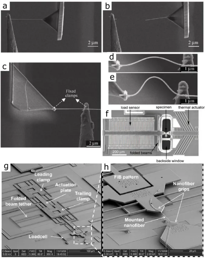
lower than that of a bulk polycrystalline Pd, which was explained by grain boundary relaxation and creep. Another feature revealed by the test is that the yield stress of the NWs was much higher than that of nanocrystalline Pd in bulk form. This phenomenon was attributed to the lowered defect density in nanoscale. Naraghi et al. developed a MEMS test platform with off-chip actuation for mechanical characterization of polymeric nanofibers in ambient conditions under optical microscope [53]. Engineering stresses and strains were obtained directly from images of the MEMS platform, by extracting the relative rigid body displacements of the device components by digital image correlation. The accuracy in determining displacements by this optical method was shown to be better than 50 nm. This technique enables the mechanical characterization of NWs composed of electron beam sensitive materials. E.g. physical aging and cross-linking in polymeric fibers subjected to the SEM electron beam do not permit its use. In the application of this method, the mechanical behavior of electrospun polyacrylonitrile nanofibers with diameters ranging from 300 to 600 nm was investigated. The stress-strain curves demonstrated an apparent elastic-perfectly plastic behavior with elastic modulus of 7.6 GPa and large irreversible strains that exceeded 220 %. They improved the MEMS test platform using on-chip actuation and the results on polyacrylonitrile nanofibers agreed well with off-chip measurements (Fig. 11g-h) [54].
30
Figure 11. SEM images taken during the tensile test of a ZnO NW with diameter of 20 nm (a-b). Fracture occurs on the NW when the applied load reaches a certain value (fracture load) (b). SEM images showing the buckling test of a ZnO NW with diameter of 46 nm (c-e) (images a-e adapted from [51]). In situ SEM and TEM tensile testing device including actuator, load sensor, and specimen (f) (image f adapted from [52]). SEM images of the on-chip actuated MEMS platform for nanomechanical experiments under ambient conditions (g-h) (images g-h adapted from [54]).
31 1.3.3. Atomic force microscopy based methods
AFM is also a promising tool for the mechanical investigation of NWs/NRs/NTs, since cantilever deflections and torsions and hence normal and lateral forces (NFs and LFs) acting on the tip are precisely monitored by the position sensitive photo detector (PSPD). Therefore AFM is capable of applying and detecting NFs and LFs in nano-Newton range. Similarly to axial loading AFM based methods are not restricted to the elastic properties. Bending can be performed by applying NFs or LFs on the individual nanostructures by the tip of the AFM cantilever. Due to the finite radius of curvature of the tip bending by NFs can be performed only in the case of NWs with diameters significantly higher than the dimensions of the tip.
Otherwise the tip would slip off from the NW to be measured. From this aspect, the application of LFs seems more general-purpose, however, the main weak point of the latter is that the lateral output of the PSPD has to be well calibrated in order to obtain fair results. In the usually applied indirect calibration methods many error sources exist, therefore the elastic parameters in the literature have to be carefully handled.
Wong et al. used the AFM to determine the mechanical properties of individual horizontal SiC NRs and multiwalled carbon NTs pinned at one end to the surface of the substrate by exerting lateral loads by the tip of the AFM cantilever [55]. The bending force was measured versus displacement along the unpinned lengths. The carbon NTs were about two times as stiff as the SiC NRs. Continued bending of the SiC NRs ultimately led to fracture, whereas the NTs exhibited an interesting elastic buckling process. The strengths of the SiC NRs were substantially greater than those found previously for larger SiC structures, and approached theoretical values.
Paulo et al. examined the mechanical elasticity of Si NWs [56], which were grown horizontally between the two facing Si(111) sidewalls of microtrenches prefabricated on a Si(110) substrate, resulting in suspended single and double clamped nanowire-in-trench structures. The deflection of the NWs was induced and measured by the controlled application of NFs with the AFM tip. The agreement between the NW deflection measurements and the theoretical behavior of single and double clamped elastic beams demonstrated the overall elastic beamlike behavior. Ni et al. performed nanoscale three-point bending tests directly on individual horizontal amorphous SiO2 NWs bridging a trench by exerting normal loads with the AFM tip (Fig. 12a) [57]. The NWs were double clamped by electron beam-induced deposition. Elastic modulus of the amorphous SiO2 NWs was measured to be 76.6 GPa,
32
which is close to the reported value of the bulk SiO2. The NWs exhibited brittle fracture failure in bending.
Wu et al. studied the mechanical behavior of double clamped Au NWs of different diameters [58]. The horizontal NWs were bridging a trench, similarly to the above methods, however, they applied lateral loads instead of a normal indentation (Fig. 12b, f-g). They found that the Young's modulus is essentially independent of diameter and very close to the bulk value, whereas the yield strength is largest for the smallest diameter wires, with strengths up to 100 times that of bulk materials, and substantially larger than that reported for bulk nanocrystalline metals. Wen et al. performed controlled LF AFM measurement of the mechanical properties of double clamped ZnO NWs in the same arrangement [59]. They have demonstrated that contrary to most of the reports the Young's modulus is diameter independent and close to the bulk value down to diameters of 18 nm. The tensile strength of these materials increased for small diameter wires approaching values of 7.00 GPa, which is consistent with reduced levels of defect incorporation as the materials dimensions are reduced. The latter measurement was also carried out in situ inside a SEM by Celik et al. [60].
They incorporated a customized AFM into the vacuum chamber of the SEM in order to establish the visibility of bending and breaking Ni NWs (Fig. 12c-e). Experimental results revealed that Ni NWs have significantly higher yield strengths than their bulk counterparts, although their elastic modulus values are comparable to bulk Ni modulus values.
The experiment carried out by Song et al. on perpendicularly standing ZnO NWs is also based on the LF analysis, however, it fundamentally differs from the above detailed methods [21].
The AFM tip was scanning over the surface in contact mode (Fig. 12h), and they acquired simultaneously the topography and LF image of the aligned NWs. The elastic modulus of the individual NWs was derived from the images (Fig. 12i-j). For the [0001] ZnO NWs/NRs grown on a sapphire surface with an average diameter of 45 nm, the elastic modulus was measured to be 29 GPa.
33
Figure 12. NW deflections obtained on a suspended SiO2 NW during a nanoscale three-point bending test (a) (image a adapted from [57]). Schematic of a double clamped wire in a lateral bending test with an AFM tip (b).
AFM image taken after elastic manipulation of a 200 nm thick Au NW (f) using the method sketched in (b), and AFM image obtained after plastic manipulation (g) (images b and f-g adapted from [58]). SEM micrograph of an AFM cantilever mounted in a customized AFM located in the SEM, which is bending NWs suspended over a trench (c). SEM image of a Ni NW suspended over a trench (d), and the same NW after fracture (e) (images c-e adapted from [60]). Procedures for measuring the elastic modulus of a vertical NW in the AFM contacting mode (h). Topography image (i) and LF image (j) of aligned ZnO NW arrays received in AFM contacting mode. The elastic modulus of each NW in the scanning range can be derived from these images (images h-j adapted from [21]).
34 1.3.4. Other nanomechanical methods
In the following I briefly discuss a few other methods, which cannot be classified in any of the above techniques.
Li et al. measured the hardness and elastic modulus of horizontal Ag NWs lying on a glass substrate by applying a nanoindenter [61]. The indenter tip was used to image and locate the Ag NWs and then in situ indent them with the same tip. The indentation impression was also imaged with the same tip (Fig, 13e). Post-test imaging provided the ability to verify that the test was performed in the anticipated location, which maximizes the reliability of the data.
The hardness and elastic modulus were calculated from the load-displacement curve. It was found that the Ag NWs have comparable hardness and elastic modulus to bulk Ag.
A nanomanipulator arm equipped with an AFM cantilever offers a perfect tool to carry out static bending tests on one-end-affixed NWs/NRs/NTs in situ inside a SEM. Hoffmann et al.
manipulated individual vertical ZnO NWs with a calibrated AFM tip mounted on a nanomanipulator arm [62]. The substrate with the NWs was mounted on a piezo stack. The coarse positioning of the AFM tip toward the sample was done with the robotic arm and the fine positioning, as well as the manipulation of the NWs, was achieved by moving the sample with the piezo stack. They carried out static bending (Fig. 13a-c) and tensile experiments.
Hence the displacements of the AFM probe corresponded to the bending and tensile forces.
The fracture strain in the bending test was found to be of 7.7 % and revealed a strength about twice as high as in the tensile test. From the tensile experiments, the Young‟s modulus could be measured to be within 30% of that of bulk ZnO. Manoharan et al. applied bending loads on one-end-affixed ZnO NWs using a tipless AFM cantilever with known spring constant mounted on a manipulator to determine the Young's modulus (Fig. 13d) [63]. The NWs were oriented perpendicular to the edge of a silicon wafer and glued at the end near the edge of the wafer by focused ion beam-induced Pt deposition. Young‟s modulus was measured to be about 30% of the modulus value at the bulk scale.
Marszalek et al. formed Au NW columns by pressing a gold-coated AFM tip against a gold- coated coverslip [64]. The NW could be compressed by a few nanometers and then stretched back by moving a piezoelectric actuator that pushed or pulled the NW against the AFM cantilever (Fig. 13f). During these cycles, the forces applied to the NW were measured and its length was also monitored. NWs elongated and shortened under force in quantized steps. The
35
results were explained by the sliding of crystal planes within the Au NWs creating stacking faults that change the local structure from face-centered cubic to hexagonal close packed.
Figure 13. SEM micrographs showing a sequence of an in situ bending experiment performed on a vertical ZnO NW: images recorded before any deformation (a), right before fracture (b), and after fracture (c) (images a-c adapted from [62]). Superimposed SEM images from the in situ bending of a ZnO NW showing the specimen and only the edge of the loading cantilever (d) (image d adapted from [63]). AFM image of indents on a silver NW (e) (image e adapted from [61]). Schematic of the experimental set-up used to capture quantized plastic deformation in gold NWs (f) (image f adapted from [64]).
Table 2 summarizes the experimentally determined Young‟s modulus/bending modulus values of NWs/NRs/NTs of different materials with the bulk values for comparison. The data are adapted from the papers introduced in subsections 1.3.1., 1.3.2., 1.3.3., and 1.3.4.
![Figure 1. Atomic lattice of ZnO wurtzite crystal showing the tetrahedral coordination of the Zn and O atoms (a) (image a adapted from [3])](https://thumb-eu.123doks.com/thumbv2/9dokorg/872162.46905/12.892.108.785.218.507/figure-atomic-lattice-wurtzite-crystal-showing-tetrahedral-coordination.webp)
![Figure 3. SEM image showing an array of ZnO NRs grown by the aqueous chemical method onto a ZnO nanostructured thin film (image adapted from [25])](https://thumb-eu.123doks.com/thumbv2/9dokorg/872162.46905/16.892.283.611.814.1093/figure-image-showing-aqueous-chemical-method-nanostructured-adapted.webp)
![Figure 4. Side (a) and top (b) cross-section of the potential distribution for a ZnO NW with a diameter of 50 nm and a length of 600 nm at a lateral bending force of 80 nN as the result of finite element calculation (images a-b adapted from [31])](https://thumb-eu.123doks.com/thumbv2/9dokorg/872162.46905/18.892.120.783.121.557/figure-section-potential-distribution-diameter-lateral-bending-calculation.webp)
![Figure 7. Tilted-view (a) and top-view (b) SEM micrographs of ZnO NWs on sapphire substrate forming natural laser cavities (images a-b adapted from [37])](https://thumb-eu.123doks.com/thumbv2/9dokorg/872162.46905/22.892.116.787.108.465/figure-tilted-micrographs-sapphire-substrate-forming-natural-cavities.webp)
![Figure 12. NW deflections obtained on a suspended SiO 2 NW during a nanoscale three-point bending test (a) (image a adapted from [57])](https://thumb-eu.123doks.com/thumbv2/9dokorg/872162.46905/33.892.117.787.112.786/figure-deflections-obtained-suspended-nanoscale-point-bending-adapted.webp)
