Gate-Controlled Supercurrent in Epitaxial Al/InAs Nanowires
Tosson Elalaily, Olivér Kürtössy, Zoltán Scherübl, Martin Berke, Gergö Fülöp, István Endre Lukács, Thomas Kanne, Jesper Nygård, Kenji Watanabe, Takashi Taniguchi, Péter Makk,* and Szabolcs Csonka*
Cite This:Nano Lett.2021, 21, 9684−9690 Read Online
ACCESS
Metrics & More Article Recommendations*
sı Supporting InformationABSTRACT: Gate-controlled supercurrent (GCS) in supercon- ducting nanobridges has recently attracted attention as a means to create superconducting switches. Despite the clear advantages for applications, the microscopic mechanism of this effect is still under debate. In this work, we realize GCS for the first time in a highly crystalline superconductor epitaxially grown on an InAs nanowire.
We show that the supercurrent in the epitaxial Al layer can be switched to the normal state by applying≃±23 V on a bottom gate insulated from the nanowire by a crystalline hBN layer. Our
extensive study of the temperature and magneticfield dependencies suggests that the electricfield is unlikely to be the origin of GCS in our device. Though hot electron injection alone cannot explain our experimentalfindings, a very recent non-equilibrium phonons based picture is compatible with most of our results.
KEYWORDS: field effect, epitaxial superconductors, nanowire, gate-controlled supercurrent, hot electron injection, phonons
■
INTRODUCTIONSuperconducting circuits have become promising building blocks in various architectures for quantum computing devices,1,2 single photon detectors,3,4 quantum-limited ampli- fiers,5 phase-coherent caloritronics,6,7 ultrasensitive magneto- meters8,9 and fast classical supercomputers.10,11In the latter, the superconducting electronics are integrated with semi- conductor technology. In particular, rapid singleflux quantum (RSFQ) devices become more desirable than semiconducting switches due to their fast switching speed and low power consumption.10 Since RSFQ consists of a flux-controlled superconducting loop with Josephson junctions along with on- chip coils, its upscaling remains a challenge. In order to realize scalable superconducting switches, electrical control via gate electrodes would be desirable.
Very recently a striking new effect was observed in metallic nanostructures. In superconducting nanobridges the super- current can be controlled by applying a voltage on a closely spaced gate electrode.12−24 By increasing the gate voltage beyond a certain threshold, the supercurrent in the nanobridge can be quenched. Previous works show GCS in thin metallic nanowires,12,18,22,23
in proximitized normal metal in a super- conductor−normal−superconductor (SNS) junction13and in Dayem nanobridges.15,17,20 In addition to high-speed super- conducting switches,23observation of GCS in superconducting nanostructures led to the realization of new nanodevices such as gate-controlled superconducting phase shifter16 and half- wave nanorectifiers.20Despite the clear advantages of GCS for applications, the origin of the effect is still under debate. Some works explained the suppression of the supercurrent by an electric field induced perturbation of the superconducting
state,25−27such as, e.g., by Swinger effect,28others attributed the effect to injection of high-energy quasiparticles tunneling from the gate electrode.22−24 Even though the microscopic origin of the effect is unclear, gate-controlled nanobridges can work at ultralow power and high switching speed. In addition, their configuration can be easily scaled up, which provides a promising building block for superconducting switches in modern architectures of both classical and quantum com- puters.
Recently InAs semiconductor nanowires with epitaxial Al superconducting shells29have become the primary platform for research on various potential quantum devices. Concepts have been developed for topologically protected qubits30 and surface code for majorana states31based on hybrid nanowires, and they are also promising for realization of gatemon or Andreev qubits.32,33 In all of these examples of quantum hardware, the gate tunable superconductivity would be highly desirable to provide an additional experimental control knob of the system. However, up to now, all gate tuning experiments were performed on polycrystalline materials and therefore it has not been clear if GCS exists for highly crystalline materials.
In this work, we studied for thefirst time the superconducting gating effect in highly crystalline Al shells epitaxially grown on
Received: September 8, 2021 Revised: October 20, 2021 Published: November 2, 2021
© 2021 The Authors. Published by
Downloaded via CENTER FOR ENERGY RESEARCH on January 13, 2022 at 10:27:11 (UTC). See https://pubs.acs.org/sharingguidelines for options on how to legitimately share published articles.
InAs nanowires.29 We will show in the following that the superconducting state can be switched offby applying voltage on a nearby metallic electrode and provide detailed character- istics of the gating behavior.
■
RESULTS AND DISCUSSIONWe have used InAs nanowires grown by molecular beam epitaxy (MBE) using gold nanoparticles as catalysts. After InAs nanowires growth, an Al shell layer of thickness 20 nm was epitaxially grown by deposition within the MBE chamber at low temperature. By rotating the substrate during Al growth, the Al shell layer is grown in all InAs nanowire facets, resulting in fully covered nanowires.29
To investigate the gate-controlled supercurrent in InAs nanowires with epitaxial superconducting layer, first, we fabricated devices with the standard geometry using side gates12−23 or a backagte,12 where the gating effect was observed in eight devices. In order to improve the geometry, i.e., minimize the separation between the gate and the nanowire and keep the leakage current small, we developed the geometry presented in Figure 1a−c. A metallic gate from Ti/Au (yellow) with thicknesses of 7/33 nm was fabricated on an intrinsic Si wafer with a 290 nm thick oxide layer. To insulate the gate from the wire, 20−30 nm thick hBN (pink) was stacked on the gate electrode with PDMS-based dry transfer technique. hBN is an excellent single crystal insulator between the gate and the wire, serving as a tunnel barrier.34−38 The nanowire (gray) with Al shell (green) was deposited by a micromanipulator on top of the hBN layer. Two pairs of Al contacts (blue) have been fabricated on the top of the nanowire with a distance of 1.5 μm to allow quasi-four-probe measurements. More details about fabrication are given in Methods (see theSupporting Information).
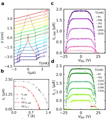
The current−voltage (I−V) characteristics of the nanowire device measured at 40 mK clearly show a well developed zero resistance state (see green curve in Figure 1d) corresponding to a supercurrentflowing through the Al shell of the wire. Two clear switches to a finite resistance state are observed at 1.94 and 2.34 μA. Similar multiple transitions were observed in a suspended Ti nanowire.18 The nanowire device shows a hysteretic behavior and switches back at two successive retrapping current values at Ir,1= 1.94 μA andIr,2 = 1.74μA when the measurements were carried out in the opposite ramping direction. To identify the origin of the two switching steps, we have separately measured the I−V curves for each horizontal pair of contacts (blue electrodes inFigure 1a) using a two-probe method. The measurements for the top pair with blue curve switch at 2.34 μA, while the bottom electrodes switch at 7.5μA (see theSupporting Information). From this, we could attribute the switching at the lower current to the SC- normal transition of the epitaxial Al shell, IC,NW, while the switching at the higher current is the same as that of the Al contact segment above the nanowire,IC,C, which is marked by the red rectangle in Figure 1a.
The dependence of the supercurrent on the gate voltage was investigated by measuring the I−V curve of the nanowire device as a function of the bottom gate voltage, VBG (see Figure 2a). The white regions represent the zero resistance state. With increasing VBG with either negative or positive polarity, both IC,NW and IC,C remain constant. Beyond the threshold atVBG≃±12 V, both critical currents are suppressed together up to full suppression at the critical gate voltage,VBGC
≃±23 V, at which the device is switched to the normal state.
The maximum electric field estimated at the critical gate voltage isEmax≈ 200 MVm−1, which is in the same order of magnitude as that reported in refs18 and 39. The fine characteristics of theI−Vcurves are better visible inFigure 2b, where the red and gray dashed lines trace the suppression of IC,NWandIC,Cwith increasingVBG, respectively. We note that with increasing VBG, the difference between the retrapping current Ir,2and IC,Cis decreased and fully vanished at VBG≈
±22 V.
The leakage current, Ileak, from the gate to the nanowire device was also measured within a±VBGCwindow by recording the voltage across the pre-resistor on the gate (seeFigure 1a).
The leakage current was then corrected by subtracting the leakage between lines of the cryostat (see Supporting Information).23 The measured Ileak shows an exponential increase with VBG for both polarities (see Figure 2c), noting that, a strong increase is seen in the leakage current around the gate voltages, where the supercurrents get suppressed.
The critical temperature was determined by measuring the I−V characteristics of the device at different elevated Figure 1.Device configuration. (a) False colored SEM image of the fabricated device with schematics of the device circuit. Schematic of the device with (b) 45° angle view and (c) side view. (d) I−V characteristics of the nanowire device (green curve) at 40 mK with two different switchings atIC,NWandIC,Cin the case of bias current is ramped from negative to positive values (solid green arrow). In the opposite ramping direction (dotted green arrow), it switches back at two successive retrapping current values,Ir,1andIr,2. Measurement of the top pair of Al contacts using the two-probe method (blue curve), showing the switching of the contacts at the same value ofIC,C.
temperatures atVBG= 0 (seeFigure 3a). In the case ofIC,NW, it is fully quenched atTC,NW≃1050 mK, while forIC,CatTC,C≃ 1400 mK with corresponding normal state resistancesRn,NW= 135ΩandRn,C= 191Ω, respectively. By extracting the values of IC,NW and IC,C, the dependence of the critical currents on temperature is plotted in Figure 3b. The red dashed−dotted and gray dotted curves arefits of the temperature dependences of IC,NW and IC,C, respectively, by using the Ambegaokar− Baratoffrelation:40−42
I R e T T
T 2 ( ) tanh ( )
C n 2k
B
i
kjjjjj y
{zzzzz
= πΔ Δ
(1) where
T a T
( ) (0) tanhi TC 1
kjjjjj y
{zzzzz
Δ = Δ −
(2) is the superconducting gap at temperature T,43−45 Rn is the normal-state resistance, and kB is Boltzmann constant. The temperature dependences of both IC,NW and IC,C are fitted using the coefficienta= 2 and 2.4 and Rn = 130 and 143Ω, respectively. The latter values of the normal-state resistances are in good agreement with our experimentalfindings.
The temperature dependence of GCS has been investigated by measuring the critical currents,IC,NWandIC,Cas a function of bipolar gate voltage at elevated temperatures (see Figure 3c,d, respectively). With increasing of the bath temperature, bothIC,NWandIC,Cat zero gate voltage respect the temperature dependence of critical currents shown inFigure 3b. However, the gating characteristics look quite similar at all temperatures.
The critical gate voltage, VBGC, in the case of IC,NW did not change with increasingTup to close to its critical temperature atTC,NW, while in the case ofIC,C, it only shifts to lower values (indicated by red arrow) for measurements at temperatures higher than TC,NW. A similar shift of VBGC with increasing temperature was observed in ref18. We have also plotted the
critical currents as a function of leakage current for different temperatures (see the Supporting Information). A small change in the critical leakage current is visible due to fluctuations in the leakage current.
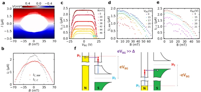
The dependence of critical currents with magneticfield was investigated by measuringI−Vcharacteristics of the nanowire device as a function of out of plane magneticfield,B, as shown inFigure 4a. BothIC,NWandIC,Cdecrease in the magneticfield, as expected. Moreover, it can be also seen thatIC,NWandIC,C cross each other at B ≃ ±24 mT, and their corresponding critical fields are BC,NW = 66 mT and BC,C = 50 mT, respectively. This is clearly seen inFigure 4b, which shows the magnetic field dependence of critical currents extracted from measurements inFigure 4a.
The dependence of GCS in the nanowire device in finite magneticfield shows a similar dependence as its temperature dependence: that the gate dependence has the same general trend at all magneticfields up to 46 mT as shown inFigure 4c in the case ofIC,C. On the other hand,VBGCdecreases whenB values approachBC,C. In the same way,IC,NWshows a similar magneticfield dependence (see theSupporting Information).
We have also measured both critical currents,IC,NWandIC,C, as a function of the magneticfield at different gate voltages up to values very close toVBGC. A significant shift inBC,NWandBC,C to smaller values is observed by increasingVBGhigher than 15 Figure 2. Gating of supercurrent. (a) I−V characteristics of the
nanowire device as a function of bipolar voltage applied to the bottom gate, VBG, as the current was sweeping from negative to positive values. (b) High-resolution I−V curves measured at selected gate voltages and equally separated ony-axis for better visibility. The red and gray dashed lines trace the suppression of IC,NW and IC,C with increasing VBG, respectively. (c) Measured and corrected leakage current from bottom gate to nanowire device as a function ofVBG.
Figure 3. Temperature dependence. (a)I−V characteristics of the nanowire device at elevated temperatures up to 1400 mK and equally separated on y-axis for better visibility. Red and gray dashed lines trace the suppression of both IC,NW and IC,C with increasing temperature, respectively. IC,NWis fully quenched at critical temper- ature TC,NW ≃ 1050 mK, while IC,C at TC,C ≃ 1400 mK. (b) Temperature dependence of IC,NW and IC,Cextracted from panel a.
Temperature dependence of the critical currents is fitted by using Ambegaokar−Baratoffrelation illustrated by the red dashed−dotted and the gray dotted lines forIC,NWandIC,C, respectively. (c, d) Critical current as a function of bipolar gate voltage for bothIC,NWandIC,Cat elevated temperatures up to 98% of their critical temperatures, respectively.
V as illustrated inFigure 4d,e, respectively. Similar dependence with B field was observed in Ti-based superconducting nanostructures.12,15 We also note that a large scattering in the critical currents values was observed in the measurements atVBG> 17 V, which can be attributed to the wide nonthermal switching current distribution as a result of the gating effect.19,24,39,46
In previous studies, the origin of GCS was attributed to two different mechanisms, either to the effect of the applied electric field12−21,25−28 or to high-energy quasiparticle injection via tunneling.22−24 We will compare our experimental findings with these explanations in the following.
GCS has been reported in various device geometries of evaporated polycrystalline metallic nanobridges made of different superconducting materials,12−21 and an explanation based on electric field induced distortion of the super- conducting wave function that could destroy the BCS state has been proposed,25−27such as, e.g., by Swinger effect.28The observedBfield andTdependencies of the gating effect show characteristics very similar to our epitaxial superconductor case. However, there is afinite leakage current of≈100 pA at gate voltages where the supercurrent is reduced (see Figure 2a,c). This leakage current is largely B-field and temperature independent, as expected (see the Supporting Information).
Assuming that the leakage takes place between the gate electrode and the nanowire, in the simplest ballistic picture, hot electrons are injected into the superconducting shell with energies even as high as 10−20 eV, which is several orders of magnitude higher than the SC gap. These electrons could heat up the superconducting bridge and drive it to the normal state, as it is proposed by refs22−24as a microscopic origin of the gating effect. Our basic estimation (see the Supporting Information) of induced heat transfer also suggests that the hot electrons could bring the temperature of the epitaxial shell
in the range of the superconducting critical temperature.
Instead of using silicon dioxide or other amorphous insulators, the gate electrode and the superconductor are separated by a 20−30 nm thick single crystalline hBN layer in our device, which is a large band gap insulator commonly used as a tunnel barrier in 2D electronics.34,35,38 Considering a tunnel barrier between the gate and superconductor, the heating effect resulting from hot electron injection should show a strong asymmetric dependence on the polarity of the gate voltage. For the polarity when electrons tunnel from the gate electrode to the superconductor (see Figure 4f (left)), hot electrons relax their energy in the superconductor by inducing a large number of quasiparticles, which results in a significant heat load. On the other hand, for opposite polarity (see Figure 4f (right)), hot electrons heat the metal block of a large gate electrode, which has a much smaller heating effect on the superconductor isolated by the gate insulator. Such gate voltage asymmetry was observed in ref22(see Figure 6 in the extended data for the reference). However, it does not appear in our measurements (see Figure 2a) after the initial training period (see the Supporting Information), which contradicts the simple explanation based on ballistic injection of hot electrons.
Nevertheless, we should also consider within this comparison the difference in the device geometry between the investigated device (in ref22) and the device presented here in our work.
However, if the tunneling process is not ballistic through the hBN, inelastic processes could lead to dissipation within the barrier itself, resulting in more symmetric I−V curves. These inelastic excitations could most likely be phonons, as explained at the end of this section. However, in suspended nanobridges presented in ref18, the leakage current and the generation of inelastic excitations are suppressed by orders of magnitude, so the gating effect in these devices could have another origin besides the injection of hot electrons/phonons.
Figure 4.Magneticfield dependence and schematic of ballistic hot electron injection. (a)I−Vcharacteristics of the nanowire device as a function of out of plane magneticfield. (b) Critical currents of the nanowire device and the contact interface region as a function of the applied magnetic field, extracted from the measurements in panel a.IC,NWandIC,Ccross each other atB≃±24 mT, leading to corresponding critical magneticfields, BC,NW= 66 mT andBC,C= 50 mT, respectively. (c)IC,Cas a function of bipolar gate voltage at magneticfields up to 46 mT. (d, e)IC,NWandIC,Cas a function of magneticfield at gate voltage values close to the critical gate voltage, respectively. (f) Schematic diagrams of ballistic electron injection from/to the metallic gate N to/from the superconducting nanowire device S in the left and right panels, respectively. Colored/uncolored parts represent occupied/unoccupied states. As the hot electron (red circle) tunnels, it will relax to the lowest unoccupied state, releasing heat on either the N or S side, resulting in different heating of the S side as the polarity ofVBGchanges.
Considering the magnetic field dependence at finite gate voltage (Figure 4d,e), it is consistent with hot electron injection, since increasing the gate voltage leads to an increase in the energy and rate of high-energy electrons injected into the nanowire segment. As a result, the device heats up more and the criticalfield of the superconducting wire decreases to smaller values. Moreover, as the magneticfield increases, the critical temperature of the superconductor decreases. In turn, a smaller gate voltage could bring the electronic temperature of the device up to this reduced critical temperature of the superconductor. This is visible in Figure 4c, where the reduction of the critical gate voltage is shown.
Finally, we focus on theTdependence ofVBGC. In a simple hot electron injection scenario, one would expect that at elevated temperatures, a lower heat load would be sufficient to drive the contact segment to normal state. However, our results show that VBGCfor the nanowire does not depend on the temperature up to TC,NW. This alone would be consistent with an electricfield-based origin. At temperatures larger than TC,NW, the nanowire is in the normal state and only the contacts are superconducting. As shown by the red arrow on Figure 3d,VBGCdecreases at higher temperatures, as expected from Joule heating scenarios. We note that above TC,NW the wire itself is already resistive, thus current flow induces additional dissipation, which could also contribute.
In summary, the temperature dependence cannot be described by a simple ballistic injection of hot electrons alone, but the strong dependence on the leakage current also makes the origin due to an electricfield unlikely.
At the end we note a parallel work of Ritter et al.,39in which the authors investigated the origin of the gating effect on TiN nanowires. They found that the decrease in supercurrent for their devices was independent of the electricfield between the wire and the gate electrode. The suppression of the supercurrent was attributed to the generation of non- equilibrium phonons due to relaxation of high-energy electrons in the substrate. The generated phonons could propagate through the substrate over distances that exceed 1 μm. Once these high-energy phonons reach to the superconducting device, they generate a large number of quasiparticles and suppress the supercurrent. A similar scenario is likely to be present in our device, where the phonons spread through the hBN layer and suppress the supercurrent in the nanowire and contact segments. Moreover, this scenario explains, for example, the symmetry of GCS with gate voltage present in our measurements. The observed magnetic field and temper- ature dependencies are also compatible with heat transfer via phonons.
To sum up, the phonon generation scenario might explain most of ourfindings; however, it is likely that the origin of the GCS effect depends heavily on the device architecture, since, e.g., for suspended devices of ref 18, another origin might be present. In order to achieve reliable, fast, and integrated superconducting electronics based on GCS, further detailed studies on the various existing experimental platforms are required.
■
CONCLUSIONSIn summary, we have demonstrated the superconducting gating effect in an epitaxially grown superconducting layer for the first time. We developed a novel gate-controlled super- current transistor using an Al shell around an InAs nanowire, which acts as the active region. The device shows a full
suppression of the supercurrent by applying ≃±23 V on a bottom gate insulated from the nanowire by a high-quality single crystalline hBN layer. Detailed magnetic field and temperature dependent characterization allowed us to compare the experimental facts with existing scenarios of super- conducting gating. The gating effect independent of the polarity suggests that the simple ballistic hot electron injection does not provide a complete explanation of the observed gating. However, the strong correlation between the suppression of the critical current and the increase in the leakage current suggests that the electric field is unlikely an origin of the gating effect in our particular device. Phonon generation in the tunnel barriers, however, can give an explanation which is consistent with most of our findings.
Besides the fundamental interest, our results open the way to integrate superconducting switches into novel Al/InAs-based hybrid quantum architectures.
■
ASSOCIATED CONTENT*sı Supporting Information
The Supporting Information is available free of charge at https://pubs.acs.org/doi/10.1021/acs.nanolett.1c03493.
Methods used in device fabrication and experiments, measurement of the other pair of the contacts, correction of the leakage current, correlation between the leakage current and the critical current, magnetic field dependence of the nanowire segment, influence of temperature and magnetic field on the leakage current, theoretical model, and initial training measurements (PDF)
■
AUTHOR INFORMATION Corresponding AuthorsPéter Makk −Department of Physics and Nanoelectronics
“Momentum”Research Group of the Hungarian Academy of Sciences, Budapest University of Technology and Economics, 1111 Budapest, Hungary; orcid.org/0000-0001-7637- 4672; Email:makk.peter@ttk.bme.hu
Szabolcs Csonka−Department of Physics and Nanoelectronics“Momentum” Research Group of the Hungarian Academy of Sciences, Budapest University of Technology and Economics, 1111 Budapest, Hungary;
Email:csonka.szabolcs@ttk.bme.hu Authors
Tosson Elalaily−Department of Physics and Nanoelectronics
“Momentum”Research Group of the Hungarian Academy of Sciences, Budapest University of Technology and Economics, 1111 Budapest, Hungary; Department of Physics, Faculty of Science, Tanta University, 31527 Tanta, Gharbia, Egypt;
orcid.org/0000-0003-3595-4798
Olivér Kürtössy−Department of Physics and Nanoelectronics
“Momentum”Research Group of the Hungarian Academy of Sciences, Budapest University of Technology and Economics, 1111 Budapest, Hungary; orcid.org/0000-0003-0221- Zoltán Scherübl403X −Department of Physics and Nanoelectronics
“Momentum”Research Group of the Hungarian Academy of Sciences, Budapest University of Technology and Economics, 1111 Budapest, Hungary; UniversitéGrenoble Alpes, CEA, Grenoble INP, IRIG, PHELIQS, 38000 Grenoble, France
Martin Berke −Department of Physics and Nanoelectronics
“Momentum”Research Group of the Hungarian Academy of Sciences, Budapest University of Technology and Economics, 1111 Budapest, Hungary
Gergö Fülöp− Department of Physics and Nanoelectronics
“Momentum”Research Group of the Hungarian Academy of Sciences, Budapest University of Technology and Economics, 1111 Budapest, Hungary
István Endre Lukács−Center for Energy Research, Institute of Technical Physics and Material Science, H-1121 Budapest, Hungary
Thomas Kanne−Center for Quantum Devices and Nano- Science Center, Niels Bohr Institute, University of Copenhagen, DK-2100 Copenhagen, Denmark
Jesper Nygård− Center for Quantum Devices and Nano- Science Center, Niels Bohr Institute, University of Copenhagen, DK-2100 Copenhagen, Denmark
Kenji Watanabe−Research Center for Functional Materials, National Institute for Material Science, Tsukuba 305-0044, Japan; orcid.org/0000-0003-3701-8119
Takashi Taniguchi− International Center for Materials Nanoarchitectonics, National Institute for Materials Science, Tsukuba 305-0044, Japan; orcid.org/0000-0002-1467- 3105
Complete contact information is available at:
https://pubs.acs.org/10.1021/acs.nanolett.1c03493
Author Contributions
T.E. and O.K. contributed equally to this work. T.E., O.K., and I.E.L. fabricated the devices, T.E., O.K., Z.S., M.B. and G.F.
performed the measurements and did the data analysis. T.K.
and J.N. grew the wires. K.W. and T.T. provided the high- quality hBN. All authors discussed the results and worked on the manuscript. P.M. and Sz.Cs. guided the project.
Notes
The authors declare no competingfinancial interest.
■
ACKNOWLEDGMENTSThis work has received funding from Topograph FlagERA, the SuperTop QuantERA network, SuperGate Fet Open, and the FET Open AndQC, and from the OTKA FK-123894 grants.
This research was supported by the Ministry of Innovation and Technology and the National Research, Development and Innovation Office within the Quantum Information National Laboratory of Hungary and by the Quantum Technology National Excellence Program (Project No. 2017-1.2.1-NKP- 2017-00001), by the UNKP-20-5 New National Excellence Program, the János Bolyai Research Scholarship of the Hungarian Academy of Sciences, by the Carlsberg Foundation, and by the Danish National Research Foundation. K.W. and T.T. acknowledge support from the Elemental Strategy Initiative conducted by the MEXT, Japan, Grant No.
JPMXP0112101001, and JSPS KAKENHI, Grant Nos.
19H05790 and JP20H00354.
■
(1) Devoret, M. H.; WallraREFERENCES ff, A.; Martinis, J. M. Superconducting qubits: A short review. arXiv Preprint (Condensed Matter: Mesoscale and Nanoscale Physics), 2004. https://arxiv.org/abs/cond-mat/0411174(accessed 2021-02-13).
(2) Krantz, P.; Kjaergaard, M.; Yan, F.; Orlando, T. P.; Gustavsson, S.; Oliver, W. D. A quantum engineeras guide to superconducting qubits.Appl. Phys. Rev.2019,6, 021318.
(3) Wang, Z.; Miki, S.; Fujiwara, M. Superconducting nanowire single-photon detectors for quantum information and communica- tions.IEEE J. Sel. Top. Quantum Electron.2009,15, 1741−1747.
(4) Natarajan, C. M.; Tanner, M. G.; Hadfield, R. H. Super- conducting nanowire single-photon detectors: physics and applica- tions.Supercond. Sci. Technol.2012,25, 063001.
(5) Aumentado, J. Superconducting parametric amplifiers: The state of the art in Josephson parametric amplifiers. IEEE Microwave Magazine2020,21, 45−59.
(6) Giazotto, F.; Martínez-Pérez, M. J. The Josephson heat interferometer.Nature2012,492, 401−405.
(7) Fornieri, A.; Giazotto, F. Towards phase-coherent caloritronics in superconducting circuits.Nat. Nanotechnol.2017,12, 944.
(8) Cleuziou, J.-P.; Wernsdorfer, W.; Bouchiat, V.; Ondarçuhu, T.;
Monthioux, M. Carbon nanotube superconducting quantum interfer- ence device.Nat. Nanotechnol.2006,1, 53−59.
(9) Luomahaara, J.; Vesterinen, V.; Grönberg, L.; Hassel, J. Kinetic inductance magnetometer.Nat. Commun.2014,5, 4872.
(10) Soloviev, I. I.; Klenov, N. V.; Bakurskiy, S. V.; Kupriyanov, M.
Y.; Gudkov, A. L.; Sidorenko, A. S. Beyond Mooreas technologies:
operation principles of a superconductor alternative. Beilstein J.
Nanotechnol.2017,8, 2689−2710.
(11) Frasca, S.; Charbon, E. Hybrid superconductor-semiconductor electronics.Nature Electronics2019,2, 433−434.
(12) De Simoni, G.; Paolucci, F.; Solinas, P.; Strambini, E.; Giazotto, F. Metallic supercurrent field-effect transistor.Nat. Nanotechnol.2018, 13, 802−805.
(13) De Simoni, G.; Paolucci, F.; Puglia, C.; Giazotto, F. Josephson Field-Effect Transistors Based on All-Metallic Al/Cu/Al Proximity Nanojunctions.ACS Nano2019,13, 7871−7876.
(14) Paolucci, F.; De Simoni, G.; Solinas, P.; Strambini, E.; Puglia, C.; Ligato, N.; Giazotto, F. Field-effect control of metallic superconducting systems.AVS Quantum Science2019,1, 016501.
(15) Paolucci, F.; De Simoni, G.; Solinas, P.; Strambini, E.; Ligato, N.; Virtanen, P.; Braggio, A.; Giazotto, F. Magnetotransport Experiments on Fully Metallic Superconducting Dayem-Bridge Field-Effect Transistors.Phys. Rev. Appl.2019,11, 024061.
(16) Paolucci, F.; Vischi, F.; De Simoni, G.; Guarcello, C.; Solinas, P.; Giazotto, F. Field-Effect Controllable Metallic Josephson Interferometer.Nano Lett.2019,19, 6263−6269.
(17) De Simoni, G.; Puglia, C.; Giazotto, F. Niobium Dayem nano- bridge Josephson gate-controlled transistors. Appl. Phys. Lett.2020, 116, 242601.
(18) Rocci, M.; De Simoni, G.; Puglia, C.; Esposti, D. D.; Strambini, E.; Zannier, V.; Sorba, L.; Giazotto, F. Gate-Controlled Suspended Titanium Nanobridge Supercurrent Transistor.ACS Nano2020,14, 12621−12628.
(19) Puglia, C.; De Simoni, G.; Giazotto, F. Electrostatic control of phase slips in Ti Josephson nanotransistors.Phys. Rev. Appl.2020,13, 054026.
(20) Puglia, C.; De Simoni, G.; Ligato, N.; Giazotto, F. Vanadium gate-controlled Josephson half-wave nanorectifier. Appl. Phys. Lett.
2020,116, 252601.
(21) Puglia, C.; De Simoni, G.; Giazotto, F. Gate control of superconductivity in mesoscopic all-metallic devices.Materials2021, 14, 1243.
(22) Alegria, L. D.; Bøttcher, C. G.; Saydjari, A. K.; Pierce, A. T.;
Lee, S. H.; Harvey, S. P.; Vool, U.; Yacoby, A. High-energy quasiparticle injection into mesoscopic superconductors.Nat. Nano- technol.2021,16, 404−408.
(23) Ritter, M.; Fuhrer, A.; Haxell, D.; Hart, S.; Gumann, P.; Riel, H.; Nichele, F. A superconducting switch actuated by injection of high-energy electrons.Nat. Commun.2021,12, 1266.
(24) Golokolenov, I.; Guthrie, A.; Kafanov, S.; Pashkin, Y. A.;
Tsepelin, V. On the origin of the controversial electrostatic field effect in superconductors.Nat. Commun.2021,12, 2747.
(25) Mercaldo, M. T.; Giazotto, F.; Cuoco, M. Spectroscopic Signatures of Gate-Controlled Superconducting Phases.arXiv Preprint
(Condensed Matter: Superconductivity), 2020. arXiv:2012.01490.
https://arxiv.org/abs/2012.01490(accessed 2020-12-29).
(26) Mercaldo, M. T.; Solinas, P.; Giazotto, F.; Cuoco, M.
Electrically tunable superconductivity through surface orbital polar- ization.Phys. Rev. Appl.2020,14, 034041.
(27) Chirolli, L.; Cea, T.; Giazotto, F. Impact of electrostatic fields in layered crystalline BCS superconductors. Physical Review.Research 2021,3, 023135.
(28) Solinas, P.; Amoretti, A.; Giazotto, F. Sauter-Schwinger Effect in a Bardeen-Cooper-Schrieffer Superconductor.Phys. Rev. Lett.2021, 126, 117001.
(29) Krogstrup, P.; Ziino, N.; Chang, W.; Albrecht, S.; Madsen, M.;
Johnson, E.; Nygård, J.; Marcus, C. M.; Jespersen, T. Epitaxy of semiconductor-superconductor nanowires. Nat. Mater. 2015, 14, 400−406.
(30) Prada, E.; San-Jose, P.; de Moor, M. W.; Geresdi, A.; Lee, E. J.;
Klinovaja, J.; Loss, D.; Nygård, J.; Aguado, R.; Kouwenhoven, L. P.
From Andreev to Majorana bound states in hybrid superconductor- semiconductor nanowires.Nature Reviews Physics2020,2, 575−594.
(31) Plugge, S.; Landau, L.; Sela, E.; Altland, A.; Flensberg, K.;
Egger, R. Roadmap to Majorana surface codes.Phys. Rev. B: Condens.
Matter Mater. Phys.2016,94, 174514.
(32) Larsen, T. W.; Petersson, K. D.; Kuemmeth, F.; Jespersen, T.
S.; Krogstrup, P.; Nygård, J.; Marcus, C. M. Semiconductor-nanowire- based superconducting qubit.Phys. Rev. Lett.2015,115, 127001.
(33) Hays, M.; De Lange, G.; Serniak, K.; Van Woerkom, D.;
Bouman, D.; Krogstrup, P.; Nygård, J.; Geresdi, A.; Devoret, M.
Direct microwave measurement of andreev-bound-state dynamics in a semiconductor-nanowire josephson junction. Phys. Rev. Lett. 2018, 121, 047001.
(34) Britnell, L.; Gorbachev, R. V.; Jalil, R.; Belle, B. D.; Schedin, F.;
Katsnelson, M. I.; Eaves, L.; Morozov, S. V.; Mayorov, A. S.; Peres, N.
M.; Castro Neto, A. H.; Leist, J.; Geim, A. K.; Ponomarenko, L. A.;
Novoselov, K. S. Electron tunneling through ultrathin boron nitride crystalline barriers.Nano Lett.2012,12, 1707−1710.
(35) Fu, W.; Makk, P.; Maurand, R.; Bräuninger, M.;
Schönenberger, C. Large-scale fabrication of BN tunnel barriers for graphene spintronics.J. Appl. Phys.2014,116, 074306.
(36) Kamalakar, M. V.; Dankert, A.; Bergsten, J.; Ive, T.; Dash, S. P.
Enhanced tunnel spin injection into graphene using chemical vapor deposited hexagonal boron nitride.Sci. Rep.2015,4, 6146.
(37) Kammhuber, J.; Cassidy, M. C.; Zhang, H.; Gül, O.; Pei, F.; De Moor, M. W.; Nijholt, B.; Watanabe, K.; Taniguchi, T.; Car, D.;
Plissard, S. R.; Bakkers, E. P. A. M.; Kouwenhoven, L. P. Conductance quantization at zero magnetic field in InSb nanowires. Nano Lett.
2016,16, 3482−3486.
(38) Bretheau, L.; Joel, I.; Wang, J.; Pisoni, R.; Watanabe, K.;
Taniguchi, T.; Jarillo-Herrero, P. Tunnelling spectroscopy of Andreev states in graphene.Nat. Phys.2017,13, 756−760.
(39) Ritter, M.; Crescini, N.; Haxell, D.; Hinderling, M.; Riel, H.;
Bruder, C.; Fuhrer, A.; Nichele, F. On the Role of Out-of-Equilibrium Phonons in Gated Superconducting Switches. arXiv Preprint (Condensed Matter: Superconductivity), 2021. arXiv:2106.01816.
https://arxiv.org/abs/2106.01816(accessed 2021-06-12).
(40) Ambegaokar, V.; Baratoff, A. Tunneling between super- conductors.Phys. Rev. Lett.1963,10, 486.
(41) Joo, S.; Kim, J.-J.; Yoo, J.; Park, M.; Lee, K.; Gu, G.; Lee, J.
Cooper Pair Density of Bi2Sr2CaCu2O8+ x in Atomic scale at 4.2 K.
Nano Lett.2019,19, 1112−1117.
(42) Senkpiel, J.; Dambach, S.; Etzkorn, M.; Drost, R.; Padurariu, C.;
Kubala, B.; Belzig, W.; Yeyati, A. L.; Cuevas, J. C.; Ankerhold, J.; Ast, R.; Kern, K. Single channel Josephson effect in a high transmission atomic contact.Commun. Phys.2020,3, 131.
(43) Gross, F.; Chandrasekhar, B.; Einzel, D.; Andres, K.; Hirschfeld, P.; Ott, H.; Beuers, J.; Fisk, Z.; Smith, J. Anomalous temperature dependence of the magnetic field penetration depth in super- conducting UBe 13.Z. Phys. B: Condens. Matter1986,64, 175−188.
(44) Senapati, K.; Blamire, M. G.; Barber, Z. H. Spin-filter Josephson junctions.Nat. Mater.2011,10, 849−852.
(45) Zhang, J.; Ding, Z.; Huang, K.; Tan, C.; Hillier, A. D.; Biswas, P. K.; MacLaughlin, D. E.; Shu, L. Broken time-reversal symmetry in superconducting Pr 1- x La x Pt 4 Ge 12.Phys. Rev. B: Condens. Matter Mater. Phys.2019,100, 024508.
(46) Basset, J.; Stanisavljević, O.; Kuzmanović, M.; Gabelli, J.; Quay, C.; Estève, J.; Aprili, M. Gate-Assisted Phase Fluctuations in All- Metallic Josephson Junctions. arXiv Preprint (Condensed Matter:
Superconductivity), 2021. arXiv:2107.05375. https://arxiv.org/abs/
2107.05375(accessed 2021-07-23).