Application of Self-Organizing Maps for Technological Support of Droplet Epitaxy
Antal Ürmös
1, Zoltán Farkas
1, Márk Farkas
2, Tamás Sándor
3, László T. Kóczy
4, Ákos Nemcsics
11Institute of Microelectronics and Technology, Óbuda University Tavaszmező utca 17, H-1084 Budapest, Hungary
2Nexogen Ltd., Alkotás u. 53, H-1123 Budapest, Hungary
3Institute of Instrumentation and Automation, Óbuda University Tavaszmező utca 17, H-1084 Budapest, Hungary
4Department of Automation, Széchenyi István University Egyetem tér 1, H-9026 Győr, Hungary
E-mails: urmos.antal@kvk.uni-obuda.hu, farkas.zoltan@kvk.uni-obuda.hu, farkas.mark@nexogen.hu, sandor.tamas@kvk.uni-obuda.hu, koczy@sze.hu, nemcsics.akos@kvk.uni-obuda.hu
Abstract: The subject of this paper is the self-organized grouping of droplet epitaxial III-V- based nano-structures. For the nano-structure grouping, our developed algorithm - called Quantum Structure Analyzer 1.0 - is used. The operation of this software is based on the principles of the Kohonen Self-Organizing Network. Here, three possibilities for nano- structured groupings are shown. On one hand, we examine the classification of nano- structures with Kohonen Self-Organizing Maps, on the other hand, fuzzy inference systems are applied for the same goal. In the case of the fuzzy methods two approaches are examined in detail. According to the first fuzzy inference approach, the shape factor is calculated from the size of nanostructures. According to the second fuzzy inference approach, the shape factor calculation is based on the controllable parameters of the growth process (eg. pressure and the temperature of the substrate).
Keywords: nanostructure; classification; self-assembling; Kohonen SOM; fuzzy inference system; shape factor
1 Introduction
Recently, semiconductor nanostructures are being intensely examined in basic research as well as in applied science. The importance of epitaxially grown, low- dimensional nano-structures, is well recognizable on the yield improvement of electronic devices (eg. LEDs, lasers, solar cells). These technologies may also have impact on the development of radically new computers, such as, quantum
computers. These nano-structures are manufactured mainly with molecular beam epitaxy (MBE) technology. The features and functioning of these devices depend on the type, shape, size and spatial distribution of the contained nano-structures.
For this reason, it is essential to know the impact the technological parameters have on the qualities of the above mentioned nano-structures.
A good example for the application of these nanostructures is in the manufacturing of high efficiency solar cells. There are two developing applications for solar cells. One of them is the search of the highest efficiency for solar cells (e.g. for space exploration applications). The GaAs-based solar cells containing quantum wells (η > 40%) or quantum dots (η > 60%) belong to this group [1] [2].
There are papers from several authors on solar cells created by using intermediate- band quantum dot (QD) structures. These QD layers are between the two usual p and n layers. The band structure is shown in (Figure 1A). The photon current on these junctions is added to the usual current between the valence band and conductance band. In this way, a very high efficiency can be achieved [3] [4] [5].
The total band gap of an optimal intermediate-band QD solar cell is 1.95 eV, which is divided into two sub band gaps. The width of the higher band gap is EL (Figure 1B) and the width of the lower band gap EH is 1.24 eV. As an intermediate band, the allowed energy levels of the QDs can be used. The solar cell operating this way was described in year of 2004. On Figure 1C, the layers of this cell can be seen. In that solar cell InAs QDs were grown in GaAs matrix by MBE with the Stransky-Krastanov mode.
The nanostructures mentioned in this section are prepared by droplet epitaxy (DE), which is described later. Although the DE process was developed in detail by a team led by Koguchi at the beginning of the 90s [6] [7], publications already covered the subject between 1985 and 1991. Figure 2. indicates the number of publications on this DE method. As it can be seen, the number of relevant publications exponentially grows between 1985 and 2016.
These nanostructures can be grown using MBE equipment and a DE process [6].
Several shaped nano-structures can be formed by DE such as QDs, quantum rings (QRs), double quantum rings (DQRs), and nano-holes (NHs).
The process starts with depositing a metallic component from column of III onto a substrate (eg. on GaAs) (Figure 3). The deposited material forms droplets on the substrate surface. The next stage is the crystallization of the material from the column of V. In this second step, different types of nano-structures are formed depending on the physical parameters of the process (eg. temperature of the sample and arsenic pressure)[8].
Figure 1
(A.)The band diagram of intermediate-band QD solar cell. EG is the band gap, EL and EH are sub-bandgaps. The CB QFL is the quasi Fermi niveau of conductance band and VB QFL is
the quasi Fermi niveau of valence band. (1) and (2) stand for photon absorption under the band gap, (3) stands for photon absorption above the band gap. Source [4]. (B) IB and monogap efficiency diagram as a function of EL sub-bandgap. (C) The layer diagram of
IBQD solar cell.
Figure 2
Number of publications on droplet epitaxy between 1985 and 2016
Figure 3
Formation of nanostructures during droplet epitaxy process (source: [8])
The characteristics of nano-structures during the formation process depend on several variables. In the case of low-temperature and high background arsenic pressure, QDs are formed. The size, the spatial density and the distribution of Ga droplets can be controlled by Ga flux, Ga coverage and the temperature of the substrate. The morphology of the nano-structure can also be controlled by substrate temperature and background pressure of arsenic as well [7].
During the growth process, it is essential to know the technological parameters (eg. arsenic pressure, substrate temperature and Ga flux), for the types of nano- structures formed and the details of this formation process. The clarification of these issues is facilitated by our developed software called “Quantum Structure Analyzer 1.0”. The operation of this software is based on Kohonen’s Self- Organizing Network [9].
2 Clustering Quantum Structures
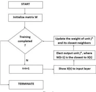
The goal of this paper is to establish a grouping or clustering of quantum structures with regard of the above mentioned technological parameters. Several technological factors exert an influence on the formation of a single nano- structure. Moreover, the type determination of a nano-structure is not a simple task. The quick recognition, that is, the transition based on the physical appearance of the structure from one type to the other is continuous. This makes ordering a given nano-structure to one type or to another, on the basis of a simple rule is impossible. For that reason, different types are identified by neural networks. These networks are not programmed in the usual rule based system applications, but are trained to recognize clusters. The training can be supervised or unsupervised. A good example for unsupervised learning techniques is the self- organizing map (SOM). It is an artificial topographic mapping inspired by neuro- biological research [10].
The topological arrangement is created by multiple repetitions of the following process (Figure 4).
Figure 4 Flowchart of Kohonen SOM
3 Classifying Quantum Structures with Fuzzy Inference System
A possible way to classify quantum structures is to define a shape factor. Because of the continuous transition between different types of nano-structures, the shape factor can be calculated with the help of fuzzy logic.
Fuzzy logic is based on the fact, that a two valued (true/false) logic, is inappropriate to emulate human thinking and it is also inappropriate to describe certain phenomena. Thus, fuzzy logic uses intermediate values, between true and false. There are statements that where it is impossible to decide if they were true or false, but intermediate values indicate the ’degree of truth’. This was the reasoning behind the invention the fuzzy logic by L. Zadeh in the 1960s [12] [13].
A X fuzzy set can be defined by a so-called membership function. This Membership functions relate a value from the interval [0,1] to every value of the x base set. The value between 0 and 1 reflects the “extent” to which the given x value is a member of the X fuzzy set:
𝛾𝑥∈ 𝑋 → [0,1] (1)
where 𝛾𝑥 is the membership function of 𝑋 fuzzy set, that unequivocally defines the set. There are different types of membership functions, in this paper we use the most frequent triangular and trapezoid shapes [12] [13].
One application of the theory described above is the fuzzy inference system.
These systems are based on a rule base model. This model consists of fuzzy sets and “if-then” constructions. These systems are frequently used and they have various applications, for example [14] [15] [16] [17]. There are many types of fuzzy inference system, for example Mamdani, Sugeno, Tsukamoto etc. [18]. The inference steps of the algorithm are the following:
1. Fuzzification 2. Aggregation 3. Defuzzification
In the fuzzification, the crisp data is converted into fuzzy data. During the aggregation the fuzzy sets, that represent the outputs of each rule are combined into a single fuzzy set. In the defuzzification the fuzzified data is converted back into the crisp number. There are many ways for the defuzzification, for example in case of the centroid method:
𝑥∗ =∑𝑚𝑖=1∑ 𝜇𝑐𝜇(𝑥𝑖)∗𝑥𝑖
𝑐(𝑥𝑖)
𝑚𝑖=1 , (2) 𝑚 is the quantization levels in the output, 𝑥𝑖 is the ith data, 𝜇𝑐(𝑥𝑖) is the ith membership function.
In this model, Mamdani-type fuzzy inference system is applied. In this case, the general form of the rules are the following:
𝑘: 𝐼𝐹 𝑥 𝑖𝑠 𝐴𝑖𝑘 𝐴𝑁𝐷 𝑦 𝑖𝑠 𝐵𝑗𝑘 𝑇𝐻𝐸𝑁 𝑧 𝑖𝑠 𝐶𝑙𝑘, (3)
where k = 1, 2, . . . , R, i = 1, 2, . . . , N, j = 1, 2, . . . , M and l = 1, 2, . . . , L. N, M and L are the numbers of membership functions for input and output variables, R is the number of the rules [18]. In the model, the default settings (AND operation:
MIN operator, OR operation: MAX operator, implication method: MIN operator, the aggregation: MAX operator, centroid defuzzification algorithm) are used. The details of the fuzzy model will be discussed in the next chapter.
4 Results and Discussion
The input of SOM (also referred to as „teaching data”) can be seen in Table 1.
A data vector is ordered to each sample. This vector contains the parameters of the nanostructure: the column I. is the number of the data vector; the column II. is the temperature of the substrate; the column III. is the flux of the component (Ga, In, Al, etc.); the column IV. is the surface coverage; the column V. is the arsenic pressure; the column VI. is the annealing time; the column VII. is the annealing temperature; the column VIII. is the base diameter of nano-structure; the column IX. is diameter of the ridge circle; the column X. is the distance of the substrate surface and the highest point of the nanostructure; the column XI. is the distance between the highest point of the nanostructure and the bottom point of the nanostructure; the column XII. is the spatial distribution of the nano-structures on the surface. The columns VIII. IX. X. XI. are the geometrical parameters of the nanostructure, and their interpretation will be introduced in the Figure 10.
I. II. III. IV. V. VI. VII. VIII. IX. X. XI. XII.
1 200 0.19 2.75 1.00E-04 10 350 60 0 7 0 1.20E+10
2 250 0.025 2.75 1.00E-04 10 350 107.5 0 37 0 4.40E+08
3 200 0.75 3.75 5.00E-05 1 350 50 0 5 0 3.60E+10
4 300 0.75 3.75 4.00E-06 5 300 60 40 2 2 1.50E+09
5 300 0.05 1.75 1.00E-05 0.33 300 100 40 20 15 1.30E+08
6 260 0.025 3.75 2.00E-04 10 350 167 0 50 0 1.60E+08
7 260 0.025 3.75 2.00E-04 10 350 250 0 35 0 1.60E+08
8 620 0.4 3.2 7.00E-07 5 620 350 150 25 55 8.00E+06
9 620 0.4 3.2 9.00E-07 5 620 350 150 25 45 9.00E+06
10 640 0.8 2 1.00E-07 3 640 200 200 15 82.4 9.00E+06
11 640 0.8 2.4 1.00E-07 3 640 200 200 15 91.12 9.00E+06
12 650 0.8 3.2 1.00E-07 3 600 15.8 15.8 11 22 8.00E+06
13 650 0.8 2 1.00E-07 2 650 300 200 2 62 8.00E+06
14 200 0.19 3.75 6.40E-05 10 350 60 0 7.5 0 1.50E+10
15 200 0.19 3.75 5.00E-05 1 350 60 0 7 0 1.20E+10
16 250 0.025 3.75 5.00E-05 10 350 110 0 32 0 4.40E+08
17 300 0.75 3.75 4.00E-06 5 300 80 35 3.6 3.6 1.50E+09
18 200 0.19 3.75 6.40E-05 10 350 40 0 7 0 3.60E+10
19 200 0.19 3.75 4.00E-06 10 300 60 60 2 2 1.50E+09
20 507 0.08 3.2 1.00E-07 2 620 210 200 4 16.5 7.50E+07
21 507 0.08 3.2 1.00E-07 2 620 200 200 0.5 3 1.60E+08
22 300 0.75 10.5 1.00E-06 0.33 300 40 10 3.3 3.3 1.50E+09
23 300 0.75 10.5 1.00E-06 1 300 70 30 3.3 7.3 4.50E-07
24 200 0.19 6 1.00E-06 1 350 40 40 2.5 2.5 8.00E+09
25 500 0.04 4 3.00E-09 30 500 290 150 15 25 4.50E+07
26 520 0.8 2.4 1.00E-07 0.05 520 200 100 3 16 5.00E+06
27 520 0.8 2.4 1.00E-07 0.05 520 200 100 4 24 1.25E+07
28 620 0.47 2.82 9.00E-07 3 620 160 10 0 5 4.00E+08
29 160 0.79 3.75 1.00E-04 10 350 60 0 7.5 0 2.00E+11
30 200 0.79 3.75 1.00E-04 10 350 60 0 7.5 0 9.00E+10
31 250 0.79 3.75 1.00E-04 10 350 250 0 35 0 1.00E+10
32 260 0.79 3.75 1.00E-04 10 350 250 0 35 0 8.00E+10
33 500 1 3 5.00E-09 0 600 185 54 4 21.5 4.50E+07
34 500 1 3 5.00E-09 0 620 185 54 3 20.5 4.50E+07
35 500 1 3 5.00E-09 1 620 185 64 2 19.5 4.50E+07
36 540 0.8 3.2 1.00E-06 2 620 200 100 2.5 9.5 4.00E+07
37 540 0.8 3.2 1.00E-07 2 620 200 100 2.5 16.5 9.00E+07
38 520 0.8 8 3.00E-06 2 620 200 100 2 5 5.00E+06
39 520 0.8 8 1.00E-07 2 620 200 100 2 20 1.25E+07
Table 1
Input data of self organizing mapping. The (I.) is the serial number, the (II.) is the temperature of the substrate. The (III.) is the flux of the component (Ga, In, Al, etc.), the (IV.) is the surface coverage.
The (V.) is the background pressure of arsenic, and (VI and VII respectively) the time period and temperature of annealing. The characteristic geometrial sizes of the nanostructure (diameter of base circle (VIII.), diameter of the ridge circle (IX.), the distance of the substrate and the highest point of the nanostructure (X.), the distance of the highest and lowest points of the nanostructure (XI.)) and the
spatial distribution of the nanostructures on the surface (XII.).
The Kohonen SOM is an iterative algorithm. The theory of the Kohonen SOM algorithm is applied by our developed software code named Quantum Structure Analyzer 1.0. The results of this algorithm are shown as the function of iterative steps on Figure 5. The forming of Kohonen graph can be seen after step 5 (A), after step 10 (B), after step 100 (C), after step 500 (D), after step 1000 (E) and after step 2000 (F).
On Figure 6, It can be seen that the temperature of the substrate grows vertically upward and the background pressure of the arsenic decreases statistically horizontally to the right. On Figure 7, it can be seen that component flux grows vertically upward and the surface coverage grows statistically horizontally to the right.
Figure 5
Snapshots of Kohonen Self-Organizing Maps after 5 steps (A), after 10 steps (B), after 100 steps (C), after 500 steps (D), after 1000 steps (E) and after 2000 steps (F)
Figure 6
Substrate temperature – Arsenic background pressure diagram. The temperature of the substrate grows vertically upward and the background pressure of the arsenic decreases statistically
horizontally to the right.
Figure 7
Component flux – surface coverage diagram. Component flux grows vertically upward and the surface coverage grows statistically horizontally to the right.
On Figure 8, it can be seen that temperature of annealing grows upward and the time of annealing statistically decreases to the right.
Figure 8
Temperature of annealing – Time of annealing diagram. The temperature of annealing grows upward and the time of annealing statistically decreases to the right.
The classification of nano-structures can be carried out several ways. Figure 9 displays the original classification based on the literature. The original data was obtained from many articles, for example Nemcsics et al. [19] [20] [21], Heyn et al. [22] [23], Kuroda et al. [24].
Figure 9
Original clustering of nanostructures (based on the literature)
The nano-structures were also classified according to geometrical attributes. The theory of fuzzy inference systems is applied by fuzzy inference system based geometrical quantum structure classification, which is developed in the Matlab environment, with the using of the Matlab Fuzzy Toolbox. Refer to Figure 10 for interpretation of the dimensions. An important thing is, that the interpretation of the geometrical parameters are the same in the Figure 10 part a, Figure 10 part b and Figure 10 part c as well. A is the diameter of the base circle of the nanostructure:
𝐴 = 𝐴(𝑑) = {𝑑, 𝑖𝑓 𝐶 ≥ 0,1 𝑛𝑚
0, 𝑜𝑡ℎ𝑒𝑟𝑤𝑖𝑠𝑒 (4)
The value B is the diameter of the ridge circle of the nanostructure. C is the distance of the top of the nanostructure from the substrate. D is the distance of the top of the nanostructure from the global or local minimum of the nanostructure. In Table 1, the size A corresponds to the column VIII., the size B corresponds to the column IX., the size C corresponds to the column X. and the size D corresponds to the column XI.
The shape factor can be calculated according to B, C or D. If the shape factor is defined according parameter B then QDs can be separated from QRs and from
NHs. But in this case neither the latter two cannot be separated nor the type of
“hybrid” (transitionary) nano-structures cannot be determined.
Figure 10
Geometrical dimensions of different nanostructures
The operation of the fuzzy model is based on Figure 10. In this case, the size C and the size D geometrical parameters are considered. The size C is the distance of the top of the nanostructure from the substrate. The size D is the distance of the top of the nanostructure from the global or local minimum of the nanostructure. If size D is smaller than or equal to 2 nanometer, then the structure is considered as a quantum dot. If size D is larger than 1 nanometer, but smaller or equal than C+1 nanometer, then it is a quantum ring. If size D is larger than C nanometer, then it is a nano-hole. Between 1 and 2 nanometers QD - QR hybrid, between C and C+1 nanometer QR - NH hybrid is detected. Contrary to this, if the shape factor is defined by fuzzy sets based on value of D and parameterized with value of C, then QRs and NHs can be clearly separated and type of hybrid nano structures can be identified as well (eg. QD - QR hybrid or QR - NH hybrid) (Figure 11A). The membership function of output can be seen on Figure 11B. Since it is possible that one or more rules of a rule base are true (meaning that one or more neuron fires), the result is defuzzyfied with centroid method and a real number is obtained.
Depending on the range this number fits into, the type may be QD, QR, NH, QD- QR hybrid or QR-NH hybrid. The mapping is described by if-then fuzzy rules that can be seen in Table 2. If only one of the rules is true (or one rule ’fires’ in fuzzy terminology) then the object is the nano-structure that belongs to the premise (QD, QR or NH). If two rules are true a hybrid form is obtained.
Input and condition Output
D < 2 nm quantum dot
D >= 1 nm and D =< C+1 nm quantum ring
D > C nm nano-hole
Table 2
The calculation of the shape factor is described with fuzzy rule base
Figure 11
(A) Membership function if geometrical dimensions C and D were used to calculate form factor. Areas with red border represent hybrid nanostructures (quantum dot-quantum ring hybrids or quantum ring-
nano-hole hybrids) (B) Membership functions of output. Hybrid structures are labeled on figure.
On Figure 12, the outline of classification with fuzzy inference system is shown.
The classification is based on the geometrical features of the nano-structures. It is also shown that to what extent belongs the given sample to a nanostructure class.
The 100% implies that there is a clear type of nano-structure. If the structure under consideration is a hybrid type (eg. a QD - QR hybrid) the result explains the degree of “QDness” and “QRness”. This ratio is calculated by relative error of the defuzzified output value to the limit of the relevant interval. The calculation formula is shown below.
𝑄𝐷(%) =(𝑄𝐷(𝐷𝑓−𝑄𝑅𝑚𝑖𝑛)
𝑚𝑎𝑥−𝑄𝑅𝑚𝑖𝑛)∗ 100 (5)
where Df is the crisp output of the fuzzy model (defuzzified value), QRmin is the lower limit of the “QR interval” and QDmax is the upper limit of the same interval.
QD(%) is the degree of “QDness”. The formula for “QRness” is shown below.
𝑄𝑅1(%) = 100 − 𝑄𝐷(%) =(𝑄𝐷(𝑄𝐷𝑚𝑎𝑥−𝐷𝑓)
𝑚𝑎𝑥−𝑄𝑅𝑚𝑖𝑛)∗ 100 (6)
where QR1(%) is the proportion of the quantum ring in percent and the meaning of the further variables is the analogous to those of 5.
The ratio for quantum ring-nano-hole hybrids are calculated in the same way:
𝑄𝑅2(%) =(𝑄𝑅(𝐷𝑓−𝑁𝐻𝑚𝑖𝑛)
𝑚𝑎𝑥−𝑁𝐻𝑚𝑖𝑛)∗ 100 (7)
where Df is the crisp (defuzzified) output of fuzzy model, NHmin is the lower limit of nano-hole interval and QRmax is the upper limit of quantum ring interval QR(%) is the degree of quantum “ringness”. The ratio of nanohole is shown below:
𝑁𝐻(%) = 100 − 𝑄𝑅2(%) =(𝑄𝑅(𝑄𝑅𝑚𝑎𝑥−𝐷𝑓)
𝑚𝑎𝑥−𝑁𝐻𝑚𝑖𝑛)∗ 100 (8)
where NH(%) is the degree of “NHness” and the other parameters are the same as in equation 7. This classification has two advantages. It is simple and accurate solution.
There is an additional possibility in the classification of nanostructures. If the classification is based on controllable technological parameters then it can be interpreted as an engineering tool. These parameters are the substrate temperature, the component flux, the background pressure of arsenic, the time interval and temperature of annealing. On Figure 13, the results of fuzzy inference classification to the nano-structures can be seen. The meaning of the 100%
proportion is the same as in the case of geometrical classification and the proportion calculation of the nanostructure junctions are also the same.
Figure 12
Result of clustering of nanostructures by fuzzy inference system based on the geometrical dimensions
Figure 13
Result of the clustering of nanostructures based on technological parameters substrate temperature and arsenic background pressure
There is an anomaly in line 23, because the algorithm mistakenly identifies NH as QR. This sample is unusual as NHs are formed generally above 500 ℃ and under
arsenic pressure of 10-7 Torr. In sample 23, the NH was formed at low substrate temperature Tsubstrate=300 ℃ and at medium arsenic pressure Pas= 10-6 Torr, after 1 minute of annealing at T=300 ℃ [25].
Conclusion
In this paper, we examined the clustering of nano-structures forming in an self- organizing process. The shape, size and spatial distribution of these structures determine the characteristics of devices that built of them. For this reason, it is important to know that how the technical parameters of manufacturing process effect each type of nanostructure. In this paper, a self-organized clustering algorithm based on shape factor was examined. In addition to this a few possible clustering methods were outlined. First, a clustering algorithm based on Kohonen SOM, then we combined this method with fuzzy inference algorithm. In the other case, two approaches were studied. In the first approach, the shape factor is determined by geometrical dimensions of the nano-structures. According to the second approach, the shape factor is determined by directly adjustable technological parameters (substrate temperature, arsenic background pressure, etc.).
The above described process is verified with an example of a QD based solar cell.
A possible realization of the QD contained solar cell, mentioned in the introduction is in the work of Kerestes et. al. [3]. In this example, the diameter of the base circle is between 10 and 18 nm and its height is between 2 and 5 nm. The average cell surface density is 9.7*1010 1/cm2. Related to our approximations, at this sample the substrate temperature was between 252 and 254 oC, the gallium flux was 0.025 ML/s. The ambient pressure of the arsenic component was between 5.01*10-5 and 1*10-4 Torr and the annealing time was 10 minute with a 350 oC annealing temperature applied.
References
[1] Z. Zheng, H. Ji, P. Yu, Z. Wang, "Recent Progress Towards Quantum Dot Solar Cells with Enhanced Optical Absorption," Nanoscale Res Lett, vol. 11, pp. 266-234, May. 2016.
[2] W. Jiang; C. Siming; S. Alwyn; L. Huiyun, "Quantum dot optoelectronic devices: lasers, photodetectors and solar cells," Journal of Physics D Applied Physics, vol. 48, p. 363001, 2015.
[3] C. Kerestes, S, Polly, D. Forbes, C. Bailey, A. Podell, J. Spann, P. Patel, B.
Richards, P. Sharps, S. Hubbard, "Fabrication and analysis of multijunction
solar cells with a quantum dot (In)GaAs junction," Progress in Photovoltaics Research and Applications, vol. 22, no. 11, pp. 1172–1179, 2013.
[4] A. Luque, A. Martí, C. Stanley, "Understanding intermediate-band solar cells," Nature Photonics, vol. 6, pp. 146–152, February 2012.
[5] T. NODA, T. MANO, M. ELBORG, K. MITSUISHI, K. SAKODA,
"Fabrication of a GaAs/AlGaAs Lattice-Matched Quantum Dot Solar Cell,"
J. Nonlinear Optic. Phys. Mat., vol. 19, no. 4, pp. 681-686, 2010.
[6] A. Benahmed, A. Aissat, A. Benkouider, J. P. Vilcot, "Modeling and simulation of InAs/GaAs quantum dots for solar cell applications," Optik - International Journal for Light and Electron Optics, vol. 127, no. 7, pp.
3531–3534, April 2016.
[7] N. Koguchi, S. Takahashi, T. Chikyow, "New MBE growth method for InSb quantum well boxes," Journal of Crystal Growth, pp. 688-692, 1991.
[8] S. Sanguinetti, N. Koguchi, "Droplet Epitaxy of Nanostructures," in Molecular Beam Epitaxy: From Research to Mass Production, 1st Edition.
Waltham, MA,USA: Elsevier Science, 2013, pp. 95-111.
[9] M. Farkas, L. T. Kóczy, Á. Nemcsics, "A hybrid approach on dimension reduction and fuzzy clustering of droplet epitaxial grown quantum structure experiments," , 3rd Symposium on Computational Intelligence, Győr, 2009.
[10] R. Rojas, "Kohonen Networks," in Neural Networks, A Systematic Introduction. Berlin, Germany: Springer-Verlag, 1996, pp. 391-412.
[11] T. Kohonen, Self-Organizing Maps, 3rd ed.: Springer, 2001.
[12] L. A. Zadeh, "Fuzzy sets," Information and Control, vol. 8, no. 3, pp. 338–
353, 1965.
[13] L. T. Kóczy, D. Tikk, Fuzzy systems. Budapest, Hungary, 2007.
[14] S. Wang, F.L. Chung, S. HongBin, H. Dewen, "Cascaded centralized TSK fuzzy system: universal approximator and high interpretation," Applied Soft Computing, vol. 5, no. 2, pp. 131-145, January 2005.
[15] S. Preitl R-E. Precup, "Stability and Sensitivity Analysis of Fuzzy Control Systems. Mechatronics Applications ," Acta Polytechnica Hungarica, vol. 3, no. 1, pp. 61-76, 2006.
[16] D. Ichalal, B. Marx, J. Ragot, D. Maquin, "Fault Detection, Isolation and Estimation for Takagi–Sugeno Nonlinear Systems," Journal of the Franklin Institute, vol. 351, no. 7, pp. 3651–3676, July 2014.
[17] H-Y. Li, R-G. Yeh, Yu-Che Lin, Lo-Yi Lin, Jing Zhao, Chih-Min Lin, Imre J. Rudas, "Medical Sample Classifier Design Using Fuzzy Cerebellar Model Neural Networks," Acta Polytechnica Hungarica, vol. 13, no. 6, pp. 7-24, 2016.
[18] N. Siddique, H. Adeli, Computational Intelligence: Synergies of Fuzzy Logic, Neural Networks and Evolutionary Computing.: John Wiley & Sons, 2013.
[19] Á. Nemcsics, A. Stemmann, J. Takács, "To the understanding of the formation of the III–V based droplet epitxial nanorings," Microelectronics Reliability, vol. 52, pp. 430-433, 2012.
[20] Á. Nemcsics, B. Pődör, L. Tóth, J. Balázs, L. Dobos, J. Makai, M. Csutorás, A. Ürmös, "Investigation of MBE grown inverted GaAs quantum dots,"
Microelectronics Reliability, vol. 59, pp. 60-63, 2016.
[21] Á. Nemcsics, Ch. Heyn, A. Stemmann, A. Schramm, H.Welsch, W. Hansen,
"The RHEED tracking of the droplet epitaxial grown quantum dot and ring structures," Materials Science and Engineering B, vol. 165, pp. 118-121, 2009.
[22] Ch. Heyn, A. Stemmann, A. Schramm, H. Welsch, W. Hansen, Á. Nemcsics,
"Faceting during GaAs quantum dot self-assembly by droplet epitaxy,"
Applied Physics Letters, vol. 90, no. 20, p. 203105, 2007.
[23] Ch Heyn, T. Bartsch, S. Sanguinetti, D. Jesson, W. Hansen, "Dynamics of mass transport during nanohole drilling by local droplet etching," Nanoscale Research Letters, pp. 10-67, Dec. 2015.
[24] T. Kuroda,T. Mano,T. Ochiai,S. Sanguinetti, K. Sakoda,G. Kido, N.
Koguchi, "Optical transitions in quantum ring complexes," PHYSICAL REVIEW B, vol. 72, p. 205301, 2005.
[25] K.H.P. Tung, H.W. Gao, N. Xiang, "Time evolution of self-assembled GaAs quantum rings grown by droplet epitaxy," Journal of Crystal Growth, vol.
371, no. 15, pp. 117-121, 2013.