In situ tuning of symmetry-breaking-induced nonreciprocity in the giant-Rashba semiconductor BiTeBr
Mátyás Kocsis,1Oleksandr Zheliuk,2Péter Makk,1Endre Tóvári ,1,*Péter Kun ,3Oleg Evgenevich Tereshchenko ,4,5,6 Konstantin Aleksandrovich Kokh,4,6,7Takashi Taniguchi,8Kenji Watanabe ,9Jianting Ye,2and Szabolcs Csonka1
1Department of Physics, Budapest University of Technology and Economics and MTA-BME Lendület Nanoelectronics Research Group, Budafoki út 8, 1111 Budapest, Hungary
2Zernike Institute for Advanced Materials, University of Groningen, Nijenborgh 4, 9747 AG Groningen, The Netherlands
3Institute of Technical Physics and Materials Science, MFA, Centre for Energy Research, Hungarian Academy of Sciences, P.O. Box 49, 1525 Budapest, Hungary
4St. Petersburg State University, 198504 St. Petersburg, Russia
5A. V. Rzhanov Institute of Semiconductor Physics, 630090 Novosibirsk, Russia
6Novosibirsk State University, 630090 Novosibirsk, Russia
7V. S. Sobolev Institute of Geology and Mineralogy, 630090 Novosibirsk, Russia
8International Center for Materials Nanoarchitectonics, National Institute for Materials Science, 1-1 Namiki, Tsukuba 305-0044, Japan
9Research Center for Functional Materials, National Institute for Materials Science, 1-1 Namiki, Tsukuba 305-0044, Japan
(Received 22 October 2020; revised 13 May 2021; accepted 14 July 2021; published 16 September 2021) Nonreciprocal transport, where the left-to-right-flowing current differs from the right-to-left-flowing one, is an unexpected phenomenon in bulk crystals. BiTeBr is a noncentrosymmetric material, with a giant Rashba spin- orbit coupling which presents this unusual effect when placed in an in-plane magnetic field. It has been shown that this effect depends strongly on the carrier density; however,in situtuning has not yet been demonstrated.
We developed a method where thin BiTeBr flakes are gate tuned via ionic-liquid gating through a thin protective hexagonal boron nitride layer. Tuning the carrier density allows a more than 400% variation of the nonreciprocal response in our sample. Our study demonstrates how a few-atomic-layer-thick van der Waals protection layer allows ionic gating of chemically sensitive, exotic nanocrystals.
DOI:10.1103/PhysRevResearch.3.033253
I. INTRODUCTION
Tuning the carrier density of nanostructures is essential for various applications and the exploration of exotic scientific phenomena. It lies at the heart of the operation of field effect transistors, it allows the implementation of electron optical elements in graphene [1–4], and it affects valley excitons in two-dimensional (2D) materials [5], spin relaxation [6], or the exchange coupling in spintronic devices [7]. Tuning of the carrier density is typically achieved by gate electrodes, which are separated from the nanostructure by an insulating layer. Ionic-liquid (IL) gating presents a much more effec- tive alternative, by inducing a layer of charged ions at the surface of the sample [8–10]. The large gating efficiency of IL enables, e.g., two-dimensional Ising superconductivity in semiconductor MoS2 [11–13] and promotes ferromagnetism in platinum [14].
*corresponding author: tovari.endre@ttk.bme.hu
Published by the American Physical Society under the terms of the Creative Commons Attribution 4.0 International license. Further distribution of this work must maintain attribution to the author(s) and the published article’s title, journal citation, and DOI.
However, the applicability of IL gating is limited, as it could induce changes in some systems [15,16]. In this paper we show how IL gating combined with a van der Waals pro- tective layer can be applied to chemically sensitive crystals. In particular, we will demonstrate how the exotic, nonreciprocal resistance of BiTeBr crystals can be boosted by IL gating.
First a brief introduction to the nonreciprocal resistance of BiTeBr is given, followed by a description of devices mak- ing use of a few-atomic-layer-thick hexagonal boron nitride (hBN) protection layer and IL-gating experimental results showing that the nonreciprocal resistance can be tuned by over 400%.
The study of nonreciprocal phenomena in noncentrosym- metric materials [17], such as BiTeBr, dates back decades.
The first such effect to be observed was magnetochiral dichro- ism (MChD) [18–20], in systems where both inversion and time-reversal symmetries are broken. Other effects where nonreciprocal responses play a central role include nonre- ciprocal dynamics of magnons in chiral-structure compounds such as LiFe5O8 [21] and Cu2OSeO3 [22] and nonreciprocal transport phenomena [23,24], which is the focus of this work.
In crystals without inversion symmetry, such as BiTeBr [25–27], a very surprising nonreciprocity has been observed in the presence of an in-plane magnetic field B [23]: the resistance of the sample depends on the polarity of the ap- plied voltage, as illustrated in Fig. 1(a). The source of the
FIG. 1. (a) Due to the lack of inversion symmetry of the crystal and the presence of an in-plane magnetic field, the current flowing through the sample depends on the polarity of the electric field applied [17,23]. (b) The crystal structure of BiTeBr (projected on the 001 and 1120 planes) [25–27]. The dashed lines show the border of a possible unit cell. (c) The band structure of BiTeBr assuming a two-dimensional crystal;
however, the theoretical calculations concern both two- and three-dimensional cases [23]. (d) The band structure in an in-plane magnetic field.
The direction of the magnetic fieldBy, electric fieldEx, and polarizationPare indicated. (e) Fermi surfaces near the energy minimum of the antiparallel spins, and color map of the reciprocal of the effective massm∗. The cross section of the dispersion relation is at the energy highlighted by the horizontal dashed line in (d).
nonreciprocal behavior lies in the crystal structure of BiTeBr [17], shown in Fig.1(b), belonging to theP3m1 space group.
The alternating layers of (BiTe)+ and Br− break inversion symmetry, induce a large polarizationP[27,28], and lead to giant Rashba spin-orbit interaction (SOI) [29]. The Rashba en- ergyERand wave-number offsetkRare indicated in Fig.1(c), and their fraction yields αR= 2EkRR =2 eV Å as the Rashba parameter [30,31], one of the largest in any bulk material [29]. The strong Rashba SOI causes a helical spin structure to develop [29,32,33], as indicated by the arrows in Figs.1(c) and1(d). Applying an in-plane magnetic field breaks time- reversal symmetry and distorts the dispersion relation of the conduction band, as shown in Fig.1(d). The spins parallel to the magnetic field (red) are shifted to lower energies, while the antiparallel (blue) spins are shifted up.
The Fermi surface for zero in-plane electric field E dis- torted by the magnetic fieldBis shown by the white dashed line in Fig.1(e), while for a finite field (Eor−E) perpendicu- lar toBit shifts, as indicated by the blue and yellow outlines.
Due to asymmetry introduced by the magnetic field and SOI, the electrons’ effective mass (along thexdirection) on each surface is different. As a result, the magnitude of the resulting charge currentIdepends on the direction ofE with respect to B. Specifically, it depends on the vector product [17], and the voltage-current characteristic takes the form
V =IR0(1+γP·B×I), (1) whereIandBare in plane,Pis the polarization of the crystal and is always out of plane,R0is the resistance atB=0, and γ measures the strength of the nonreciprocity. γ is related
to the carrier densityn by γ ∝ n12 [23], enabling us to tune nonreciprocity by modifying the carrier density. We note that based on Eq. (1), in this relation,I is the absolute, not rms, amplitude of the ac current.
It is important to note that the Fermi surface in Figs.1(d) and 1(e) is chosen so that the deformation due to the Rashba effect is clearly visible, but the actual Fermi sur- face is probably at higher energies and is also influenced by termination-dependent effects [27,30,31].
While external gates have been used to induce Rashba SOI in different materials, we estimate that the displacement field due to the polar crystal structure is orders of magnitude stronger than what the IL gate can generate.
II. HETEROSTRUCTURES
Due to the metallic nature and large carrier density of BiTeBr (3×10¹⁸ to 1.3×1019 cm−3), we have chosen IL gating to control the carrier density. For ionic-liquid gat- ing the sample and a separate gate electrode are covered by the IL, as shown in Fig. 2(a). A finite potential is ap- plied to the gate electrode while the sample is grounded.
This generates an accumulation of ions at the sample surface, as shown in Fig. 2(c). However, we found that BiTeBr is very sensitive to the ions of the IL, despite using N,N-diethyl-N-methyl-N-(2-methoxyethyl)ammonium bis(trifluoromethanesulfonyl)imide (DEME-TFSI) as a gating medium, for its chemical stability. As soon as a nonzero volt- age (Vg) was applied to the gate electrode, a current started
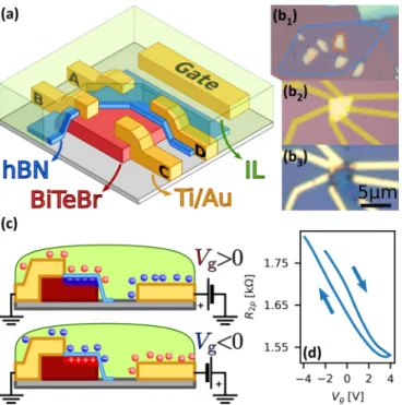
FIG. 2. (a) Schematic image of the sample, with the IL and hBN peeled away from the lower corner to show the BiTeBr flake.
(b1)–(b3) Optical images of the BiTeBr samples. (b1) The measured sample, with the BiTeBr flake (orange outline) covered with hBN (blue outline). (b2) An unprotected BiTeBr flake before liquid gat- ing, with planned electrodes. (b3) The above flake with contacts, destroyed by liquid gating. (c) Schematic image of liquid gating. Due to the metallic nature of the sample the bulk is screened, and only a thin surface layer is affected by the gating. (d) Two-point resistance as a function of the gate voltage at 220 K. The hysteretic behavior is due to the slow motion of the ions.
to flow, and the BiTeBr flakes decomposed, as shown in Fig.2(b3).
To protect the BiTeBr flakes from the IL, we developed a heterostructure where the crystal is protected by a few-atomic- layer-thick hBN flake, as shown in Figs.2(a)and2(b1). The measurements presented here were carried out on the flake outlined in orange in Fig.2(b1). As hBN is chemically stable, this technique can be used with a wide range of ILs, enabling previously incompatible materials to be used with liquid gates.
By distancing the ions from the surface the gating also be- comes more homogeneous [9].
We chose hBN flakes that were thin enough to allow for effective gating but mechanically stable enough to cover the 40–50 nm thick BiTeBr flakes. For our purpose, 3–5 nm thick flakes were selected [34]. Figure 2(b1) shows an as- sembled stack, with the hBN flake outlined in blue and the measured BiTeBr flake in orange. BiTeBr flake composition was confirmed by Raman spectroscopy and energy dispersive spectroscopy (EDS) analysis, to sort out frequently occurring impurities, as discussed in Sec.Vand AppendixD.
Ti/Au contacts were used to contact the BiTeBr flake.
Before evaporating the metallic contacts, the hBN under- neath was etched away. The same poly(methyl methacrylate) (PMMA) mask was used for the etching and the evaporation.
This ensures that the whole BiTeBr flake is covered either
FIG. 3. Second-harmonic measurements before the IL gate is applied, showing the antisymmetrized second-harmonic signal. The relative orientation of the magnetic and electric field is shown in the insets.γ can be calculated from the slope of the second-harmonic resistance using Eq. (1). As expected, no signal is detected in the parallel case.
by the electrodes or by the hBN and no ions can leak in at the hBN-electrode interface. Device fabrication is detailed in Sec.V. Preceding the heterostructures showcased here, bare BiTeBr samples were fabricated and measured without IL gating as described in AppendixA.
The two-point resistance of BiTeBr as a function of the gate voltageVg is shown in Fig.2(d). The measurement was carried out at 220 K, above the glass transition temperature of DEME-TFSI. The change in the resistance shows that the gating is successful. The leakage current through the gate electrode was continuously monitored throughout the measurement and never exceeded 0.3 nA [see AppendixB], confirming the isolation of BiTeBr from the IL by the hBN layer.
III. MEASURING THE NONRECIPROCITY Now we will turn to the measurement of the nonreciprocity.
As shown in Eq. (1), the nonreciprocity leads to the nonlin- ear current-voltage characteristics. This nonlinearity can be easily observed by applying an ac current and measuring the second-harmonic response. While other effects such as mag- netoresistance [17], or nontrivial thermoelectric behavior [35]
due to heating at the contacts, can generate second-harmonic signals of their own, all those scale with even powers of B and can be avoided by taking only the antisymmetric part of the second-harmonic resistance,R2ω= 12[R2ω(B)− R2ω(−B)]= 12R0γB×I[23].
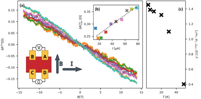
The results of our initial measurements are plotted in Fig.3, carried out before the IL was applied, at 2.5 K. The insets show the orientations of the magnetic and electric fields.R2ω
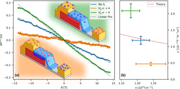
FIG. 4. (a) The magnetic field dependence of the second-harmonic signal at different gate voltages. The insets demonstrate the position of the ions in the IL and the induced density changes in the BiTeBr in the different experiments. (b)γ as a function of the carrier density extracted from Hall measurements. The dashed line shows theory from Ref. [23] without any fitting parameters. The divergence from theory can be explained by considering that the second-harmonic signal comes mainly from the gated surface layer, while the Hall measurements used for determiningnmeasure the whole crystal.
is measured as a function ofB; the value ofγ is proportional to the slope.
To verify that the measured signal originates from the nonreciprocal resistance of BiTeBr and not some other ef- fect, we took advantage of the relation from the first section, R2ω∝B×I. As Fig.3demonstrates, the signal disappears when the fields are parallel (blue curve), indicating that the source of the signal is indeed the nonreciprocal resistance of BiTeBr. Sinceγ is size dependent,γ=γAis introduced to compare different devices, whereAis the cross section of the sample perpendicular to the current’s direction. In the case of perpendicular BandE vectors (orange curve),γ=(1.2 ± 0.3)×10−13 m2T−1A−1, which is consistent with previous results [23]. The current and temperature dependence ofγ was also measured (see AppendixC). To determine the carrier density n, Hall measurements were carried out (Appendix B) and yieldedn=(1.19±0.01)×1019cm−3, which is in good agreement with the usual doping of BiTeBr [23,36]. The relation ofnandγis in good agreement with previous results [23].
Asγincreases with decreasing temperature, all measure- ments were carried out at 2.5 K.
IV. TUNING THE NONRECIPROCITY
In order to probe the density dependence ofγ, we changed the electron density, by heating the sample up above the glass transition temperature of the IL and recooling it with the IL gate set toVg= −4 V first. After measurements, the process was repeated for 4 V. The results of the second-harmonic mea- surements and densities obtained from Hall measurements are shown in Fig.4(the full Hall measurements are discussed in AppendixB). Comparing the curves in Fig.4(a), it is easy to
see that the slope of the curve, and thereforeγ, is enhanced by the gating. This is consistent with the theory, predicting γ∝ n12.
The extracted values forγas a function of carrier density are plotted in Fig.4(b). It is clearly visible that we could tune γby over 400% using IL gating in our sample within a range of 8 V.
The dashed line in Fig. 4(b)shows the results of calcu- lations based on the solution of the second-order Boltzmann equations from Ref. [23]. Although the trend in the measured values follows the theoretical expectations, the overall change inγis much stronger than expected.
The observed stronger dependence might be related to the charge carriers screening the gate-induced electric field.
Based on the measured electron density of n=1×1019 cm−3, the screening length rTF was estimated using the Thomas-Fermi approximation [37], with the assumption of a free electron gas. This yields a value ofrTF=2 nm. Since this is much shorter than the thicknessdof the BiTeBr crystal (30–40 nm), the electron density is not homogeneous verti- cally in the Rashba crystal: the gating-induced density change is more pronounced at the top of the sample and decreases farther from the surface as illustrated in the insets of Fig.4(a).
This leads to a stronger variation in the rectification effect in the top region of the sample, without significantly affecting the rest of the crystal. According to a simple two-channel model with ideal side contacts, this would lead the Hall mea- surement to be sensitive to the average carrier density, but it would not result in the effective γ deviating from what is expected [Fig.4(b)]. However, BiTeBr is a polar crystal [25,27]; thus the electron density and even the band structure could be significantly different at the surfaces [26,30,31]. On this length scale, quasiclassical approximations break down,
and the interplay of the strong gating with surface charges and termination-dependent surface states could lead to the observed deviation. Moreover, differences in top and side surface contact resistances that result from the layered nature of BiTeBr likely affect the measurement’s sensitivity to the surface and the bulk contributions.
We note that the gate-induced displacement field, as cal- culated by a simple capacitor model using a double-layer (hBN and half-screening-length-thick BiTeBr) dielectric, is orders of magnitude smaller than the built-in field related to the polarization of BiTeBr and therefore does not affect the rectification effect by itself.
A more homogeneous charge carrier density might be achieved for thinner crystals. However, usual exfoliation tech- niques failed to produce flakes thinner than 40 nm. In one of our recent works [38] we have shown that using a special exfoliation method exploiting gold surface chemistry, it is possible to exfoliate a single layer of BiTeI, which has the same crystal structure as, and very similar physical properties to, BiTeBr. With subsequent chemical etching of Au, a single layer of BiTeBr might be fabricated. Recent developments also suggest that epitaxial growth of thin BiTeBr might be possible [39]. In such flakes, ionic gating is expected to induce a significantly larger electron density change. Sinceγis pro- portional ton12, one can expect that the nonreciprocal response can be increased by orders of magnitude, as the carrier density is reduced further.
In conclusion, we have demonstrated that thin van der Waals insulator layers allow us to carry out ionic-liquid-gating experiments on crystals which are chemically unstable in ionic-liquid environments. hBN layers of 3–5 nm thickness serve as perfect protection for sensitive crystals with vertical dimensions as high as 30–50 nm, with metallic contacts cut- ting through the hBN insulator. On such a heterostructure we demonstrated the enhancement of the nonreciprocal response of the giant-Rashba spin-orbit crystal, BiTeBr. Within situ tuning the nonreciprocal response was changed by over 400%
in our sample.
These results suggest that devices with gate-tunable bulk rectification effects could be realized, even in the absence of pn junctions. Tuning of the Fermi level could also be used for spintronic applications [40]. Giant-Rashba materials are ideal candidates for spin-orbit torque devices as well [41].
It has been suggested that pressurizing BiTeBr can induce a topological phase transition [42]. It is also a promising choice for topological superconductivity when contacted with superconducting electrodes, due to the large Rashba spin-orbit coupling [43–47]. In such systems, tuning the carrier den- sity could be an important tool to enter into the topological regime.
V. METHODS
Single crystals of BiTeBr were grown by a modified Bridg- man method with rotating heat field [48]. Mixtures of binary compounds Bi2Te3 and BiBr3 were used as charges to grow BiTeBr. According to Ref. [49], BiTeBr has a congruent melt- ing point at 526◦C. Therefore a stoichiometric charge of the binary compounds was used to grow BiTeBr. Charges, sealed under vacuum in quartz ampoules, were at first prereacted at
temperatures exceeding the melting point by 20◦C and then pulled through a vertical gradient of 15◦C/cm at a rate of 10 mm/day. More technical details can be found in Refs. [48,50].
BiTeBr was exfoliated onto 290 nm SiO2-covered wafers using various blue tapes. Different environments were also ex- perimented with for the exfoliation process. While the overall number of flakes could be varied, minimal thickness was unaf- fected. Due to the thickness of the flakes, optical classification by height was not possible; atomic force microscopy (AFM) measurements were used to select the thinnest flakes.
Classification of the flakes by Raman spectroscopy was essential to verify their composition and was carried out for all flakes. Two different types of impurities were identified in the BiTeBr crystals. The first resulted in colorful flakes, sometimes as thin as 5 nm. These were electrically insulating and were identified as BiOBr based on their Raman and EDS spectra. The second type was optically indistinguishable from BiTeBr flakes; their thickness was in the same range as well.
This type of crystal did not show the nonreciprocal effects dis- cussed above, and these impurities were identified as Bi2Te3
based on their Raman [51–53] and EDS spectra. This led us to believe that the Raman spectra of BiTeBr as published by Sklyadnevaet al.[50] are in fact the spectra of Bi2Te3.
hBN flakes were exfoliated onto a Si/SiO2 chip, with an oxide layer thickness of 90 nm. The flakes were first optically classified using a bandpass filter [34], and the selected flakes were measured with AFM. Chosen flakes were transferred onto the BiTeBr flakes, using a dry transfer technique [54].
One such structure is shown in Fig. 2(b1). A PMMA layer was applied, and the design of the electrodes was exposed using electron-beam lithography. The hBN was etched away, using reactive ion etching with a mixture of CF4 [45 cubic centimeters per minute at STP (sccm)] and O2(5 sccm). This etches the hBN very quickly, without affecting the BiTeBr or the substrate, and thus the duration is not critical; usually, 15 s was chosen. Ti/Au (5 nm/60 nm) electrodes were evaporated onto the sample, using the same mask. This ensures that the etched windows in the hBN line up perfectly with the elec- trodes, sealing the BiTeBr flake away from the IL perfectly.
ncould not be measured in theVg= +4 V case as some contacts were damaged after measuring the nonreciprocal effect, and the sample became unmeasurable. The value pre- sented was estimated, by considering the change innto be the same for both gate voltages.
Measurements were carried out in a Physical Property Measurement System (PPMS) at 2.5 K using low-frequency lock-in techniques. The sample holder was equipped with a rotator which allowed us to carry out both second-harmonic (in-plane B) and Hall measurements (out-of-plane B) without heating the sample up between measurements. The IL was applied at room temperature and set at 220 K.
ACKNOWLEDGMENTS
The authors thank I. Lukacs and J. Ferenc for help in sample fabrication, S. Lenk for help with AFM measure- ments, M. G. Beckerné, F. Fülöp, and M. Hajdu for technical support, and T. Fehér and A. Virosztek. This work has re- ceived funding from the Ispintext and Topograph Flagera networks, CA16218 by COST, and from OTKA Grants No.
FK-123894 and No. NN-127900. M.K. was supported by the ÚNKP-19-3 New National Excellence Program of the Ministry for Innovation and Technology. P.M. acknowledges support from the Bolyai Fellowship, the Marie Curie grant.
This research was supported by the Ministry of Innovation and Technology and the National Research, Development and Innovation Fund of Hungary within the Quantum Informa- tion National Laboratory of Hungary and by the Quantum Technology National Excellence Program (Project Nr. 2017- 1.2.1-NKP-2017-00001). O.E.T. and K.A.K. were supported by the Russian Science Foundation (Grant No. 17-12-01047).
K.W. and T.T. acknowledge support from the Elemental Strategy Initiative conducted by MEXT, Japan, Grant No. JP- MXP0112101001, JSPS KAKENHI Grant No. JP20H00354, and CREST (JPMJCR15F3), JST. P.K. was supported by the NanoFab2D ERC Starting Grant project.
BiTeBr crystals were grown by O.E.T. and K.A.K. hBN single crystals were grown by T.T. and K.W. Samples were fabricated by M.K. and O.Z. AFM characterization was car- ried out by M.K. Raman spectroscopy was carried out by M.K.
and P.K. Measurements were carried out by M.K., O.Z., and E.T., P.M., S.Cs., and J.Y. supervised the project.
APPENDIX A: EXPERIMENTS WITHOUT IL GATING Samples where the bare BiTeBr was contacted, similar to the sample shown in Fig. 2(c), were constructed and mea- sured preceding the IL-gating experiments. The results of one such measurement are shown in Fig.5. Here, the carrier
FIG. 5. (a) Tuning the electron density with the back gate. The gating is much weaker than what is achievable with the IL gate.
(b) AFM image of the sample. The image was taken after the sample was extensively studied, and many leads have failed. The failure has caused visible damage to the two top left contacts and the bot- tom middle contact. (c) Current dependence of the second-harmonic signal. (d) Second-harmonic measurements with the current flowing parallel and perpendicularly to the magnetic field.
density was tuned with a 290 nm SiO2 back gate, which led only to a much weaker change, as shown in Fig.5(a).
Comparing it with the results shown in Fig. 4(b), we can see that the carrier density varies from one BiTeBr flake to another [23]. The current and magnetic field dependence of the second-harmonic signal was also measured and yielded γ=(6 ±1)×10−13m2T−1A−1.
APPENDIX B: FULL GATING CURVE AND HALL MEASUREMENTS
Figure6(a)shows the full IL-gating curve of the sample.Vg was ramped first to 2 V and then with each sweep successively increased to 4 V, which is still well within the electrochemical window of DEME-TFSI. The gate current was continually monitored, and it increased with increasingVg but never ex- ceeded 0.3 nA, as is shown in Fig.6(b).
When IL gating was attempted on the uncovered BiTeBr samples shown in Figs. 2(b2)–2(b3), the samples decom- posed, while smaller BiTeBr samples that were not contacted only shifted slightly as a result of the application and washing off of the IL.
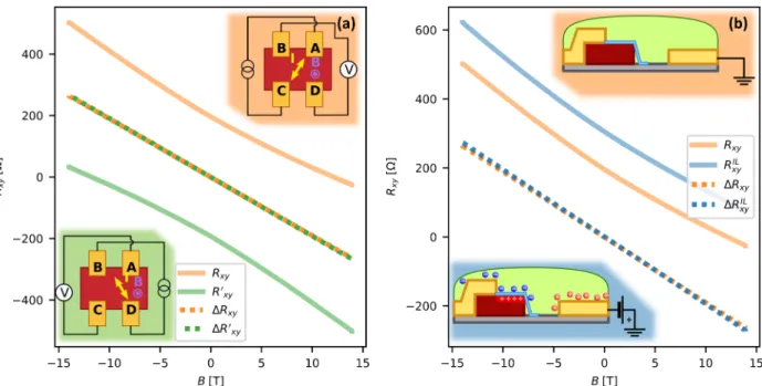
Due to the positioning of the contacts on the sample, Hall measurements could only be carried out in nonoptimal ge- ometries, as shown in the insets of Fig.7(a). This meant that instead of measuringRxy, the measured values are a mixture of Rxx andRxy. To distinguish the two components, we an- tisymmetrized the signal, yielding only the Rxy component, which was used to calculate the electron density. We note that a small error may remain due to the inhomogeneity of the current density.
We note that after the second-harmonic measurements were performed at the last gate voltage point, Vg=4 V, the Hall measurement of the average density n(Vg=4 V) could not be executed due to loss of an electrical contact.
Instead, the position of the corresponding (orange) data point in Fig. 4(b) was extrapolated. Its value may be underesti- mated: the two-channel capacitance model mentioned in the main text suggests thatVg= −4 V fully depletes the top of the BiTeBr. The positively charged depletion layer effectively decreases the capacitance atVg= −4 V, and as a result, the above extrapolation forn(Vg=4 V) is likely underestimated.
Nevertheless, this model does not describe the behavior of γ likely due to contact resistances and the effect of surface polarization, which are expected to strongly influence the gate response, as discussed in the main text, and therefore it may not be viable for density estimations, either.
APPENDIX C: CURRENT AND TEMPERATURE DEPENDENCE OF THE SECOND-HARMONIC SIGNAL
As mentioned in the main text,
R2ω∝B×Iγ. (C1) By measuringR2ωas a function ofBorI we can calculate γ. While the main text dealt exclusively with theB depen- dence, here we explore how the nonreciprocity depends on the applied current. Figure8(a)showsR2ωas a function of B, at different applied currents [5–80μA; see Fig.8(b)]. Asγ is related to the slope of the curves, we would expect the low-
FIG. 6. (a) Full gating curve at 220 K. Hysteretic behavior is due to the slow movement of the ions. Part of the same curve is shown in Fig.2. (b) Gate current as a function ofVg.Ignever exceeded 0.3 nA, and no chemical reaction takes place between the BiTeBr and the IL.
current measurements to yield significantly shallower slopes, but this is not the case. To understand the situation better, we plotted the maxima ofR2ωfrom Fig.8(a)as a function ofI in Fig.8(b). While the data could be fit with a linear function, it has a significant offset and does not cross the origin as Eq. (C1) would suggest. Since γ is calculated by dividing R2ω byI, this offset becomes more significant at small I.
To avoid the effects of this offset, all other measurements were carried out at 80–100 μA, as higher currents would have likely damaged the device. The source of this offset is not known.
The temperature dependence ofγ is shown in Fig.8(c), and it follows the same trend as the theory presented in Ref. [23].
FIG. 7. (a) Hall measurements before the IL was applied.Rxy (solid lines) and its antisymmetrized componentRxy (dotted lines) as a function of the out-of-plane magnetic field. The antisymmetrization is necessary, as the nonoptimal geometry of the sample leads to the mixing of theRxxandRxycomponents. The insets show the respective geometries for the two measurements. They both yield the same value forn.
(b) Hall measurements without the IL applied (orange) andVg= −4 V (blue). The orange curve is the same as in (a). The calculated electron densities are shown in Fig.4.
FIG. 8. All measurements were carried out at 2.5 K before applying the IL. (a)R2ω as a function of the magnetic field, for different applied current amplitudes. The nonreciprocity is expected to scale with the current as Eq. (C1) shows; the measured change is quite small, however. (b)R2Bω=15Tacquired from linear fits as a function of the applied current. While the trend is linear, it does not cross the axes at the origin; it has a 0.22offset. (c) The temperature dependence ofγfollows the same trend as the results in Ref. [23].
APPENDIX D: RAMAN SPECTRA OF BiTeBr The geometry of each sample was measured using AFM.
An AFM image of the sample discussed in the main text
is shown in the inset of Fig.9(a). The higher (white, blue) BiTeBr flakes are covered with the few-nanometer-thick hBN flake (pink). To measure the height of the BiTeBr flake, the
FIG. 9. (a) AFM image of the sample discussed in the main text. The height of the sample was measured by fitting the height distribution of the area highlighted with a dashed red rectangle. The height was measured from the top of the hBN flake to the top of the hBN+BiTeBr stack. (b) Raman spectra of different flakes obtained from the same bulk crystals during exfoliation. The gray dashed lines mark the peaks calculated using density functional theory (DFT) in Ref. [55]. The blue spectrum shows good agreement with the results of Refs. [55,56], and EDS measurements confirmed the presence of Bi, Te, and Br. The green spectrum shows good agreement with the results of Ref. [50] (where it is identified as BiTeBr) and Refs. [52,53] (where it is identified as Bi2Te3), while EDS measurements show a lack of Br. The flakes showing the orange spectrum are insulating, displaying different colors based on their thickness. The spectrum aligns with that in Ref. [57], where it is identified as BiOBr. EDS measurements confirm a lack of Te, while the excess O could not be clearly seen due to the background signal of the SiO substrate.
height distribution in the region outlined in red was measured.
As both the substrate and the BiTeBr flake are covered by the hBN, the origin was shifted to the height of the hBN layer.
From this the height of the flake is (39.0±0.6) nm.
The flakes obtained by exfoliation from the same bulk crystals could be classified into three categories. The first class is made up of white flakes 35 nm and thicker, which are conductive and show the nonreciprocal phenomena discussed in the main text. This has been confirmed on other flakes not discussed in this paper. Flakes in the second class can be thinner, from 5 nm up to more than 100 nm, are colorful and insulating. The flakes in the third class are white and thick,
resembling the first class, but do not show the nonreciprocal behavior.
To understand the cause of the differences, we carried out Raman spectroscopy and EDS measurements on all classes of flakes. Figure9(b) shows the three distinct types of Raman spectra obtained. The first class showed the expected [55,56]
Raman spectra, and the EDS confirmed the presence of Bi, Te, and Br. The second class showed the Raman spectra of BiOBr [57], and the EDS confirmed the lack of Te. The spectrum of the third class resembles that of Bi2Te3 [52,53], and EDS measurements confirmed the lack of Br.
This means that Raman spectroscopy characterization is crucial for all heterostructures.
[1] T. Taychatanapat, K. Watanabe, T. Taniguchi, and P. Jarillo- Herrero, Electrically tunable transverse magnetic focusing in graphene,Nat. Phys.9, 225 (2013).
[2] A. L. Grushina, D.-K. Ki, and A. F. Morpurgo, A ballistic pn junction in suspended graphene with split bottom gates,Appl.
Phys. Lett.102, 223102 (2013).
[3] P. Rickhaus, R. Maurand, M.-H. Liu, M. Weiss, K. Richter, and C. Schönenberger, Ballistic interferences in suspended graphene,Nat. Commun.4, 2342 (2013).
[4] P. Rickhaus, M.-H. Liu, P. Makk, R. Maurand, S. Hess, S.
Zihlmann, M. Weiss, K. Richter, and C. Schönenberger, Guid- ing of electrons in a few-mode ballistic graphene channel,Nano Lett.15, 5819 (2015).
[5] G. Wang, A. Chernikov, M. M. Glazov, T. F. Heinz, X. Marie, T. Amand, and B. Urbaszek, Colloquium: Excitons in atomi- cally thin transition metal dichalcogenides,Rev. Mod. Phys.90, 021001 (2018).
[6] F. Dettwiler, J. Fu, S. Mack, P. J. Weigele, J. C. Egues, D. D.
Awschalom, and D. M. Zumbühl, Stretchable Persistent Spin Helices in GaAs Quantum Wells, Phys. Rev. X 7, 031010 (2017).
[7] H. Ohno, D. Chiba, F. Matsukura, T. Omiya, E. Abe, T. Dietl, Y.
Ohno, and K. Ohtani, Electric-field control of ferromagnetism, Nature (London)408, 944 (2000).
[8] S. Z. Bisri, S. Shimizu, M. Nakano, and Y. Iwasa, Endeavor of iontronics: From fundamentals to applications of ion-controlled electronics,Adv. Mater. (Weinheim)29, 1607054 (2017).
[9] T. A. Petach, K. V. Reich, X. Zhang, K. Watanabe, T. Taniguchi, B. I. Shklovskii, and D. Goldhaber-Gordon, Disorder from the bulk ionic liquid in electric double layer transistors,ACS Nano 11, 8395 (2017).
[10] G. Hu, G. P. Pandey, Q. Liu, R. S. Anaredy, C. Ma, M. Liu, J. Li, S. K. Shaw, and J. Wu, Self-organization of ions at the interface between graphene and ionic liquid DEME-TFSI,ACS Appl. Mater. Interfaces9, 35437 (2017).
[11] J. M. Lu, O. Zheliuk, I. Leermakers, N. F. Q. Yuan, U.
Zeitler, K. T. Law, and J. T. Ye, Evidence for two-dimensional Ising superconductivity in gated MoS2, Science 350, 1353 (2015).
[12] Q. Chen, J. Lu, L. Liang, O. Zheliuk, A. A. E. Yumin, and J. Ye, Continuous low-bias switching of superconductivity in a MoS2 transistor,Adv. Mater. (Weinheim)30, 1800399 (2018).
[13] O. Zheliuk, J. M. Lu, Q. H. Chen, A. A. E. Yumin, S. Golightly, and J. T. Ye, Josephson coupled Ising pairing induced in suspended MoS2 bilayers by double-side ionic gating, Nat.
Nanotechnol.14, 1123 (2019).
[14] L. Liang, Q. Chen, J. Lu, W. Talsma, J. Shan, G. R. Blake, T. T. M. Palstra, and J. Ye, Inducing ferromagnetism and Kondo effect in platinum by paramagnetic ionic gating,Sci. Adv.4, eaar2030 (2018).
[15] Z. Zhang, S. Qin, K. Fu, G. Yu, W. Li, X. Zhang, S. Sun, L. Song, S. Li, R. Hao, Y. Fan, Q. Sun, G. Pan, Y. Cai, and B. Zhang, Fabrication of normally-off AlGaN/GaN metal–
insulator–semiconductor high-electron-mobility transistors by photo-electrochemical gate recess etching in ionic liquid,Appl.
Phys. Express9, 084102 (2016).
[16] M.-R. Zhang, S.-J. Qin, H.-D. Peng, and G.-B. Pan, Porous GaN photoelectrode fabricated by photo-assisted electrochemi- cal etching using ionic liquid as etchant,Mater. Lett.182, 363 (2016).
[17] Y. Tokura and N. Nagaosa, Nonreciprocal responses from non- centrosymmetric quantum materials, Nat. Commun. 9, 3740 (2018).
[18] G. L. J. A. Rikken and E. Raupach, Observation of magneto-chiral dichroism, Nature (London) 390, 493 (1997).
[19] T. Roth and G. L. J. A. Rikken, Observation of Magne- toelectric Jones Birefringence, Phys. Rev. Lett. 85, 4478 (2000).
[20] Y. Shimada, M. Matsubara, Y. Kaneko, J. P. He, and Y. Tokura, Magnetoelectric emission in a magnetic ferroelectric Er-doped (Ba,Sr)TiO3,Appl. Phys. Lett.89, 101112 (2006).
[21] Y. Iguchi, S. Uemura, K. Ueno, and Y. Onose, Nonrecipro- cal magnon propagation in a noncentrosymmetric ferromagnet LiFe5O8,Phys. Rev. B92, 184419 (2015).
[22] S. Seki, Y. Okamura, K. Kondou, K. Shibata, M. Kubota, R.
Takagi, F. Kagawa, M. Kawasaki, G. Tatara, Y. Otani, and Y. Tokura, Magnetochiral nonreciprocity of volume spin wave propagation in chiral-lattice ferromagnets, Phys. Rev. B 93, 235131 (2016).
[23] T. Ideue, K. Hamamoto, S. Koshikawa, M. Ezawa, S. Shimizu, Y. Kaneko, Y. Tokura, N. Nagaosa, and Y. Iwasa, Bulk rec- tification effect in a polar semiconductor,Nat. Phys. 13, 578 (2017).
[24] Y. M. Itahashi, T. Ideue, Y. Saito, S. Shimizu, T. Ouchi, T. Nojima, and Y. Iwasa, Nonreciprocal transport in gate- induced polar superconductor SrTiO3, Sci. Adv.6, eaay9120 (2020).
[25] A. Shevelkov, E. Dikarev, R. Shpanchenko, and B. Popovkin, Crystal structures of bismuth tellurohalides BiTeX(X=Cl, Br, I) from x-ray powder diffraction data,J. Solid State Chem.114, 379 (1995).
[26] S. V. Eremeev, I. P. Rusinov, I. A. Nechaev, and E. V. Chulkov, Rashba split surface states in BiTeBr,New J. Phys.15, 075015 (2013).
[27] S. Fiedler, T. Bathon, S. V. Eremeev, O. E. Tereshchenko, K. A.
Kokh, E. V. Chulkov, P. Sessi, H. Bentmann, M. Bode, and F.
Reinert, Termination-dependent surface properties in the giant- Rashba semiconductors BiTeX(X=Cl, Br, I),Phys. Rev. B92, 235430 (2015).
[28] L. W. Molenkamp, G. Schmidt, and G. E. W. Bauer, The Rashba Hamiltonian and electron transport,Phys. Rev. B64, 121202(R) (2001).
[29] K. Ishizaka, M. S. Bahramy, H. Murakawa, M. Sakano, T.
Shimojima, T. Sonobe, K. Koizumi, S. Shin, H. Miyahara, A.
Kimura, K. Miyamoto, T. Okuda, H. Namatame, M. Taniguchi, R. Arita, N. Nagaosa, K. Kobayashi, Y. Murakami, R. Kumai, Y. Kanekoet al., Giant Rashba-type spin splitting in bulk BiTeI, Nat. Mater.10, 521 (2011).
[30] L. Moreschini, G. Autès, A. Crepaldi, S. Moser, J. Johannsen, K. Kim, H. Berger, P. Bugnon, A. Magrez, J. Denlinger, E.
Rotenberg, A. Bostwick, O. Yazyev, and M. Grioni, Bulk and surface band structure of the new family of semiconductors BiTeX (X=I, Br, Cl), J. Electron Spectrosc. Relat. Phenom.
201, 115 (2015).
[31] M. Sakano, M. S. Bahramy, A. Katayama, T. Shimojima, H. Murakawa, Y. Kaneko, W. Malaeb, S. Shin, K. Ono, H. Kumigashira, R. Arita, N. Nagaosa, H. Y. Hwang, Y.
Tokura, and K. Ishizaka, Strongly Spin-Orbit Coupled Two- Dimensional Electron Gas Emerging near the Surface of Polar Semiconductors,Phys. Rev. Lett.110, 107204 (2013).
[32] A. A. Eremko, L. S. Brizhik, and V. M. Loktev, Spin states of Dirac equation and Rashba spin-orbit interaction,Annals of Physics,361, 423 (2015).
[33] H. Maaß, H. Bentmann, C. Seibel, C. Tusche, S. V. Eremeev, T. R. F. Peixoto, O. E. Tereshchenko, K. A. Kokh, E. V.
Chulkov, J. Kirschner, and F. Reinert, Spin-texture inversion in the giant Rashba semiconductor BiTeI,Nat. Commun.7, 11621 (2016).
[34] R. V. Gorbachev, I. Riaz, R. R. Nair, R. Jalil, L. Britnell, B. D. Belle, E. W. Hill, K. S. Novoselov, K. Watanabe, T.
Taniguchi, A. K. Geim, and P. Blake, Hunting for monolayer boron nitride: Optical and Raman signatures, Small 7, 465 (2011).
[35] R. Nakai and N. Nagaosa, Nonreciprocal thermal and thermo- electric transport of electrons in noncentrosymmetric crystals, Phys. Rev. B99, 115201 (2019).
[36] N. Ogawa, M. S. Bahramy, Y. Kaneko, and Y. Tokura, Pho- tocontrol of Dirac electrons in a bulk Rashba semiconductor, Phys. Rev. B90, 125122 (2014).
[37] J. Sólyom,Fundamentals of the Physics of Solids (Springer, Berlin, 2010).
[38] B. Fülöp, Z. Tajkov, J. Pet˝o, P. Kun, J. Koltai, L. Oroszlány, E.
Tóvári, H. Murakawa, Y. Tokura, S. Bordács, L. Tapasztó, and
S. Csonka, Exfoliation of single layer BiTeI flakes,2D Mater.
5, 031013 (2018).
[39] D. Hajra, R. Sailus, M. Blei, K. Yumigeta, Y. Shen, and S.
Tongay, Epitaxial synthesis of highly oriented 2D Janus Rashba semiconductor BiTeCl and BiTeBr layers,ACS Nano14, 15626 (2020).
[40] Z. Kovács-Krausz, A. M. Hoque, P. Makk, B. Szentpéteri, M.
Kocsis, B. Fülöp, M. V. Yakushev, T. V. Kuznetsova, O. E.
Tereshchenko, K. A. Kokh, I. E. Lukács, T. Taniguchi, K.
Watanabe, S. P. Dash, and S. Csonka, Electrically controlled spin injection from giant Rashba spin-orbit conductor BiTeBr, Nano Lett.20, 4782 (2020).
[41] A. Manchon, J. Železný, I. M. Miron, T. Jungwirth, J. Sinova, A. Thiaville, K. Garello, and P. Gambardella, Current-induced spin-orbit torques in ferromagnetic and antiferromagnetic sys- tems,Rev. Mod. Phys.91, 035004 (2019).
[42] A. Ohmura, Y. Higuchi, T. Ochiai, M. Kanou, F. Ishikawa, S.
Nakano, A. Nakayama, Y. Yamada, and T. Sasagawa, Pressure- induced topological phase transition in polar semiconductor BiTeBr,Phys. Rev. B95, 125203 (2017).
[43] H. Ren, F. Pientka, S. Hart, A. T. Pierce, M. Kosowsky, L.
Lunczer, R. Schlereth, B. Scharf, E. M. Hankiewicz, L. W.
Molenkamp, B. I. Halperin, and A. Yacoby, Topological super- conductivity in a phase-controlled Josephson junction,Nature (London)569, 93 (2019).
[44] A. Fornieri, A. M. Whiticar, F. Setiawan, E. Portolés, A. C. C.
Drachmann, A. Keselman, S. Gronin, C. Thomas, T. Wang, R.
Kallaher, G. C. Gardner, E. Berg, M. J. Manfra, A. Stern, C. M.
Marcus, and F. Nichele, Evidence of topological superconduc- tivity in planar Josephson junctions,Nature (London)569, 89 (2019).
[45] M. C. Dartiailh, W. Mayer, J. Yuan, K. S. Wickramasinghe, A.
Matos-Abiague, I. Žuti´c, and J. Shabani, Phase Signature of Topological Transition in Josephson junctions,Phys. Rev. Lett.
126, 036802 (2021).
[46] F. Pientka, A. Keselman, E. Berg, A. Yacoby, A. Stern, and B. I.
Halperin, Topological Superconductivity in a Planar Josephson Junction,Phys. Rev. X7, 021032 (2017).
[47] M. Hell, M. Leijnse, and K. Flensberg, Two-Dimensional Plat- form for Networks of Majorana Bound States,Phys. Rev. Lett.
118, 107701 (2017).
[48] K. A. Kokh, B. G. Nenashev, A. E. Kokh, and G. Y.
Shvedenkov, Application of a rotating heat field in Bridgman–
Stockbarger crystal growth,J. Cryst. Growth275, e2129 (2005).
[49] U. Petasch, C. Hennig, and H. Oppermann, Investigations on the pseudobinary system Bi2Te3/BiCl3,Z. Naturforsch., B: J.
Chem. Sci.54b, 234 (1999).
[50] I. Y. Sklyadneva, R. Heid, K.-P. Bohnen, V. Chis, V. A. Volodin, K. A. Kokh, O. E. Tereshchenko, P. M. Echenique, and E. V.
Chulkov, Lattice dynamics of bismuth tellurohalides, Phys.
Rev. B86, 094302 (2012).
[51] W. Richter and C. R. Becker, A Raman and far-infrared investigation of phonons in the rhombohedral V2–VI3 com- pounds Bi2Te3, Bi2Se3, Sb2Te3 and Bi2(Te1−xSex)3 (0<x<
1), (Bi1−ySby)2Te3 (0<y<1),Phys. Status Solidi B84, 619 (1977).
[52] L. M. Goncalves, C. Couto, P. Alpuim, A. G. Rolo, F. Völklein, and J. H. Correia, Optimization of thermoelectric properties on Bi2Te3 thin films deposited by thermal co-evaporation, Thin Solid Films518, 2816 (2010).
[53] K. M. F. Shahil, M. Z. Hossain, V. Goyal, and A. A. Balandin, Micro-Raman spectroscopy of mechanically exfoliated few- quintuple layers of Bi2Te3, Bi2Se3, and Sb2Te3 materials, J. Appl. Phys. (Melville, NY)111, 054305 (2012).
[54] A. K. Geim and I. V. Grigorieva, Van der Waals heterostruc- tures,Nature (London)499, 419 (2013).
[55] J. A. Sans, F. J. Manjón, A. L. J. Pereira, R. Vilaplana, O.
Gomis, A. Segura, A. Muñoz, P. Rodríguez-Hernández, C.
Popescu, C. Drasar, and P. Ruleova, Structural, vibrational, and
electrical study of compressed BiTeBr,Phys. Rev. B93, 024110 (2016).
[56] A. Akrap, J. Teyssier, A. Magrez, P. Bugnon, H. Berger, A. B. Kuzmenko, and D. van der Marel, Optical prop- erties of BiTeBr and BiTeCl, Phys. Rev. B 90, 035201 (2014).
[57] J. E. D. Davies, Solid state vibrational spectroscopy—III[1] The infrared and Raman spectra of the bismuth(III) oxide halides, J. Inorg. Nucl. Chem.35, 1531 (1973).
![FIG. 1. (a) Due to the lack of inversion symmetry of the crystal and the presence of an in-plane magnetic field, the current flowing through the sample depends on the polarity of the electric field applied [17,23]](https://thumb-eu.123doks.com/thumbv2/9dokorg/756620.32441/2.911.96.814.102.466/inversion-symmetry-crystal-presence-magnetic-current-polarity-electric.webp)