Low Dispersion, High Voltage, Low Leakage GaN HEMTs on Native GaN Substrates
Muhammad Alshahed, Student Member, IEEE,Lars Heuken, Mohammed Alomari, Ildiko Cora, Lajos Toth, Bela Pecz, Clemens Waechter, Thomas Bergunde, and Joachim N. Burghartz, Fellow, IEEE
Abstract—In this work the advantages of GaN HEMTs grown on native GaN substrates over GaN/Si or GaN/Sapphire sub- strates are investigated, and correlated with epitaxial quality.
TEM plane view and cross section analysis of GaN/GaN revealed dislocation density lower than 1×106cm−2, which is at least 3 orders of magnitude lower than the case of GaN/Si or GaN/Sapphire. In the case of GaN/Si, the dislocations did not necessarily originate from the substrate/nucleation layer inter- face, but the strain relief and isolation buffer stacks were main contributors to the dislocation density. GaN/GaN HEMTs demon- strated superior electrical and thermal performance. GaN/GaN demonstrated 3 orders of magnitude lower off-state leakage, current collapse (Ron increase) after stress bias less than 15%
compared to50%in the case of GaN/Si, and2%drop of the on- state current due to self-heating in DC operation as compared to 13% and 16% for GaN/Si and GaN/Sapphire respectively.
The GaN/Si thermal performance approached GaN/GaN only by substrate removal. Therefore GaN/GaN can allow high on-state current, low off-state leakage current, minimal current collapse, and enhanced thermal dissipation capability at the same time, which can be directly correlated to the absence of high dislocation densities.
Index Terms—bulk GaN, current collapse, GaN HEMT
I. INTRODUCTION
T
HE increased demand for more reliable and efficient power conversion systems [1], [2], with focus on more efficient semiconductor power switch, which being the main component in the system determines the overall performance, reliability and efficiency of the whole system [3], promotes wide bandgap semiconductors, such as Silicon Carbide (SiC) and G Gallium Nitride (GaN), as prime candidates to replace the traditional Silicon (Si) technology [4]. GaN-based High Electron Mobility Transistors (HEMTs) are considered to be the future power semiconductor switches [5], [6] at least for voltage operation range up to 650 V. However, the higher GaN cost and poorer reliability compared to Si counterparts are two major obstacles hindering the much anticipated wide commercialization of GaN power switches [7], [8]. The cost issue is addressed by the considerable development in GaN on large area Si wafers (GaN/Si) epitaxy (up to 200mm wafer diameter), which are capable of high voltage operation with relatively low leakage current [9]. However, GaN/SiM. Alshahed, L. Heuken, M. Alomari and J. N. Burghartz are with the Institut fr Mikroelektronik Stuttgart (IMS CHIPs)
I. Cora, L. Toth and B. Pecz are with the Institute of Technical Physics and Materials Science, Centre for Energy Research, Hungarian Academy of Sciences Hungary, Budapest
C. Waechter and T. Bergunde are with Azur Space Solar Power GmbH Manuscript received December 30, 2017; revised xxx, 2018.
is considered the worst case scenario in terms of epitaxy, having a larger thermal and lattice mismatch compared to the traditional GaN/sapphire or GaN/SiC, which in turn yield a higher defect density in the order of ≈10 cm−2, compared to GaN/Sapphire (≈109cm−2) and GaN/SiC (≈ 109cm−2).
Therefore, addressing the cost issue by relying on epitaxy on foreign substrates, which yield a degraded epitaxial quality compared to the ideal case of GaN grown on GaN [10], might come at the expense of increasing or complicating the reliability issues as will also be shown here.
The main reliability issues in GaN power HEMTs are the increase in dynamic on-resistance (Ron) [11], the off-state leakage currents, and the thermal management. Those main reliability issues can be traced directly to the quality of the epitaxial material [12], [13], exhibited in the dislocation den- sity, and can be reduced or eliminated with a near dislocation free material, such as GaN/GaN substrates. The increase in Ron occurs due to charge trapping, mainly in the bulk of the material in the case of DC power switching [11]. The increase in Ron has a significant impact on the device, and consequently, the whole system in terms of efficiency and switching performance [14], [15] and has to be taken into account at the system design stage. As will be argued here, reducing the current collapse (Ron increase) and at the same time decreasing the leakage currents by making the buffer layers more insulating (e.g. using compensation doping), might not be achievable at all, if the density of threading dislocations are not drastically reduced, for example by using native GaN substrates for the subsequent GaN epitaxy.
The fundamental approach of using GaN/GaN substrates instead of GaN on foreign substrates did indeed indicate an improved electrical performance [16], as was also demon- strated by the authors in an earlier publication [17]. In this work, the electrical and thermal analyses are extended and sup- plemented with structural Transmission Electron Microscopy (TEM) analysis. The significantly reduced dislocation density in GaN/GaN yielded significantly superior electronic and thermal properties of the HEMTs in DC and pulsed operation modes. In addition, it was evident that some of the strategies taken in the epitaxy of GaN/Si substrates to reduce the residual stress in the wafer and to increase the voltage operation range might inadvertently amplify the dynamicRon increase.
II. ROLE OF THREADING DISLOCATIONS INGAN HEMTS
The GaN HEMT system is based on a tight charge balance, where injection and trapping of electrons either on the surface
IEEE TRANSACTION ON ELECTRON DEVICES, VOL. 14, NO. 8, AUGUST 2017 2
of the device or in the bulk of the material (GaN buffer) is at the expense of the two dimensional Electron Gas (2DEG) den- sity. In RF applications, where low off-state voltages and high frequencies are employed, the current collapse is dominated by charge injection and trapping on the surface [18], while charge injection and trapping in the bulk is minimal. In power switching applications, however, the off-state operation voltage is much higher than in RF applications, while the operation frequencies are much lower (MHz compared to several GHz).
This induces charge injection in the bulk of the material, especially when using a conductive Si substrate, which is usually grounded, therefore introducing not only a lateral field component between the source and drain, but also a vertical component between the drain and the substrate. The current collapse in this case is dominated by bulk charges trapping, which are not released before the next switching cycle [11].
In general, in order for the carrier trapping process to occur there should exist 1) trapping centres and 2) a path through which the electrons are transported to the trapping centres. In order to minimize the current collapse, either 1) the density of trapping centres have to be minimized, or 2) the leakage paths conducting electrons to the trapping cites have to be inhibited. If this is not possible, then the detrapping process should be facilitated. A discharge path has to be made available for trapped electrons to be conducted away from the trapping centres towards the surface electrical contacts.
Trapping centres in GaN HEMT can exist at the surface, which is usually inhibited using a proper surface passivation [19], or in the bulk of the material. These can be the compen- sation doping species such as Carbon or Iron, which are used to obtain an insulating GaN buffer (denoted here as C-GaN), or at the interfaces between the nucleation layer, stress relief layer, C-GaN buffer, and the unintentionally doped GaN buffer (UID-GaN), or in dislocations and point defects. The path to charging can be background conductivity due to unintentional doping, or threading dislocations. Therefore, threading dis- locations can act as charging centres, and/or charging paths depending on their type. A considerable amount of previous work has been dedicated to investigating the effect of threading dislocations on the leakage current and dynamic performance of the GaN material system [20]. Leakage currents have been successfully imaged along screw-type threading dislocations [21], and edge-type threading dislocations have been shown to be responsible for electron trapping and mobility degradation in GaN material system [22]. Therefore, the existence of threading dislocations impacts the leakage current adversely and introduces electron trapping centres [23].
The current collapse due to charge trapping in the bulk can be modelled using a lumped-components RC equivalent circuit representing the coupling between the channel and the different trapping locations as depicted in a simplified way in Fig. 1. The equivalent circuit depicts resistive elements featuring the leakage current through the layers, either due to unintentional doping or due to conductive threading dislo- cations among other crystalline defects, whereas the capacitor elements represent the capacitive coupling between the layers.
The strain relief layers are not considered in the equivalent circuit for the sake of simplicity. In the case of GaN/Si many
stress relief layers are usually employed, in addition to a relatively thick (>2µm) C-GaN buffer layer. This however, does not prevent a high dislocation density, and therefore, the existence of trapping centres and charging paths is inevitable.
In this case, the current collapse severity can be reduced by increasing the leakage current in the channel layer towards the surface to release trapped electrons, as suggested in [24]. This implies that there would be a trade-off between the leakage current in the HEMT and the severity of the current collapse such that a simultaneous improvement in both parameters is not possible. However, this is only valid under the assumption that the limiting factor in the current collapse is the conduction to and from the trapping centres but not the trapping and detrapping process itself. Although this is true in some cases, the detrapping process of deep levels related to carbon, Ga- vacancies, N-vacancies among others could be in the order of milli-seconds to seconds depending on the position of the trap energy level within the bandgap which makes the de-trapping process itself the limiting factor [25]. This can be verified by looking at the case of an insulating substrate such as Sapphire, as will be shown here, where current injection from the back side is minimal. Here, the source of trapped electrons is not any more the substrate but in this case the free carrier concentration in the channel layer and/or the surface contacts, and the charging path is the same as the discharging path (through the channel layer and the surface of the device). The devices yet showed a significant current collapse, implying that the detrapping process of carriers is, by itself, a limiting factor.
Based on the previous discussion, one can conclude that, in order to simultaneously achieve an improvement in the leakage current and dynamic performance of GaN HEMTs, the density of dislocations, acting as both charging centres and charging paths, has to be reduced, as also shown by [26]. Current collapse would be reduced accordingly but not completely suppressed, as will be shown here. The presence of other parasitic leakage paths due to unintentionally doped layers and carrier injection from the metal electrodes, and the trapping of those carriers in lattice imperfections caused by compensation doping would still cause current collapse. Ultimately, the use of highly resistive native GaN templates would reduce the threading dislocations density to a minimum, and at the same time avoid the use of compensation doping, thus, yielding HEMTs that are current collapse free. The availability of such insulating GaN Bulk templates is, however, very limited until now.
Rsurface-channel
Rchannel-C-GaN
RC-GaN-substrate
Csurface-channel
Cchannel-C-GaN
CC-GaN-substrate
GaN Channel C-GaN
Substrate
AlGaN Gate Source
Drain
2DEG
Fig. 1. Electrical equivalent circuit of the coupling between the 2DEG channel and the most important trapping sites in the GaN material system
III. EXPERIMENTALWORK
The impact of threading dislocations on the device DC, dynamic and thermal performance is investigated through a comparative study between GaN HEMTs fabricated on GaN grown on different substrates. Semi-insulating 2-inch GaN on HVPE native GaN substrates were overgrown with 3.5µm thick C-GaN layers, followed by 400nm UID-GaN (GaN channel) and 25nm AlGaN barrier in an MOCVD reactor.
Another set of 2-inch GaN/Sapphire were overgrown with the same layers in the same reactor. In addition, externally acquired 2-inch GaN/Sapphire wafers with similar buffer and barrier properties, and 6-inch GaN/Si wafers were acquired from research oriented and commercial supplier respectively, and added to the comparison. Since it is not possible to grow the same layers of GaN interlayers and GaN buffer on both the GaN/Sapphire and GaN/GaN on one hand, and GaN/Si on the other hand, the GaN/Si wafer choice was based on meeting the specifications of minimal wafer bow, low leakage 600 V rating. All wafer types were then processed in the same process run with minimal process steps comprised only of simple test structures and HEMTs, in order not to induce material defects or degradation due to the process steps. More details about the fabrication steps and the DC device performance of the resulting devices can be found in [17]. Therefore, all 2-inch wafers include a compensated buffer layer with similar doping concentration, but vary in the dislocation density depending on the substrate type. Free areas from the processed wafers were diced and analysed by TEM using plane view and cross sections, while electrical and thermal characterization was conducted using dedicated structures.
A. Structural Investigation
The dislocation density was estimated using the TEM plane view images of the surface, as shown in Fig. 2. These are manifested by the dots on the surface. The thick white stripes are thickness contrast and are not related to the defects in the material. Using this method, the defect density was estimated to be 2.7 ×109cm−2 for GaN/Si, and 9 ×108cm−2 for GaN/Sapphire. On the other hand the dislocation density on the GaN/GaN was below the detection threshold, and therefore is estimated to be below 106cm−2. Therefore the GaN/GaN does indeed have at least 3 orders of magnitude lower defect density than GaN/Sapphire or GaN/Si. However, the defects imaged here are the defects reaching the surface of the sample, and not necessarily the defect in the bulk which could be terminated before reaching the surface. Such defect can still play a role in current collapse, if extending from the substrate to the bulk of the material. The higher structural quality of GaN/GaN is confirmed using cross sections as shown in Fig.
3, where no evidence of threading dislocations could be seen.
In the case of GaN/Sapphire, the presence of such dislocations is clear, where some are terminated before reaching the surface and some extend all the way up to the surface.
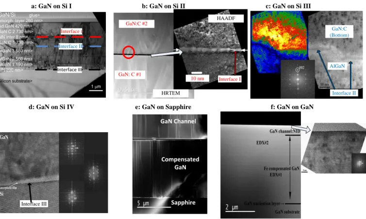
A detailed analysis has been performed for the GaN/Si due to its complicated epitaxial structure. Starting with the GaN/Si, the full epitaxial stack is shown in Fig. 3a where the multiple layers needed for the strain relief as well as
compensation doping are resolved in the TEM images. Given the large number of interfaces and for the sake of simplicity, only 3 interfaces will be discussed here. Initially, all the layers contained dislocations extending in some case all the way from the substrate to the surface. Some of the defects originate from the interfaces, such as interface I, shown in detail in Fig.
3b. This interface is composed on an AlN spacer between two C-GaN layers. Interesting to observe was the presence of voids mixed with crystalline bridges across the interface.
The AlN grows as islands, and where the islands meet they form V-shape defects, out of which a defect is initiated. At the interface between the AlGaN buffer layer and the C-GaN buffer layer, denoted here as interface II and shown in detail in Fig. 3c, defects (parallel to (001)) in the two layers are very common and could be inversion boundary or anti-phase boundary. This is seen more clearly in the colour-coded phase shift map using the 002 reflection shown in Fig. 3d.
From these observations, one can conclude that dislocations originated from inner interfaces and did not just propagate from the highly defective interface at the Si/nucleation layer interface. Fig. 3d depicts the so called Interface III which is the interface between the nucleation layer (in this case AlN) and the Si substrate. This layer is concluded to be more amorphous than crystalline. However amorphous the layer is, the subsequent growth of epitaxial layers had a crystalline structure, while some of the upper interfaces initiated a higher defect density than the bottom most interface. The defect density is reduced in the UID-buffer compared to other in- terlayers. Therefore it can be said that the strategies taken to mitigate the lattice and thermal mismatch between Si and GaN, and to achieve certain isolation specifications might be in fact a cause for increased leakage currents and deteriorated dynamic performance. The effect of the now identified defect density is correlated next to the electrical performance. In Fig.
3e-f the cross-sections of GaN/Sapphire and GaN/GaN are shown respectively. It is clear that in GaN/Sapphire threading dislocations initiate at the Sapphire/GaN interface where in GaN/GaN no trace of threading dislocations could be detected.
B. Electrical Investigation
The difference in the structural quality between the different substrates is reflected in the electrical performance of the test devices. Fig. 4 shows the DC output characteristics of a100µmHEMT with a gate length of 4µmand a gate drain distance of 15µm. It is obvious that the GaN/GaN HEMT possesses lower on-resistance, higher saturation velocity and lower self-heating and, thus, higher current density compared to those HEMTs on Si and Sapphire.
The 4-terminal DC leakage current in off-state operation of the device under high drain bias with a grounded substrate is shown in Fig. 5. In this measurement, the HEMT device is biased below pinch-off (Vgs< Vthreshold) and the drain bias is swept from 0 V up to 600 V or up to the device breakdown.
The GaN/GaN HEMT features the lowest leakage current level as compared to the other samples. This low leakage can be correlated to the significantly lower dislocation density, which acts as current conduction paths, especially if compared to
IEEE TRANSACTION ON ELECTRON DEVICES, VOL. 14, NO. 8, AUGUST 2017 4
a: GaN on GaN b: GaN on Sapphire c: GaN on Si
400 nm 400 nm
Fig. 2. Images (a), (b) and (c) depict plan view images of near the surface region of GaN/GaN substrate, GaN/Sapphire substrate and GaN/Si substrate respectively. The wide thick stripes in (a) are thickness contrast and not related to the defects in the material. Unlike (a), structural defects can be detected in (b) and (c)
a: GaN on Si I b: GaN on Si II c: GaN on Si III
d: GaN on Si IV e: GaN on Sapphire f: GaN on GaN
Interface I Interface II
Interface III
Interface III
Interface II GaN:C (Bottom)
AlGaN
Compensated GaN GaN Channel
Sapphire
GaN:C #2
GaN: C #1
Interface I 10 nm
HRTEM
HAADF
Fig. 3. TEM cross-sections of the different samples under investigation. Images (a) to (d) belong to the commercial GaN/Si sample. In (a) the full epitaxial stack is depicted with reference to 3 important interfaces that are shown in (b), (c) and (d). Image (e) depicts the TEM cross-section of the GaN/Sapphire sample and image (f) depicts that of the GaN/GaN sample as a whole and with a zoom at the AlGaN/GaN channel interface
GaN/Sapphire II, which was grown in the same reactor with similar epitaxial layer design. It is worth mentioning that this leakage represents the total leakage current in the device;
namely the vertical leakage current through the substrate and the lateral leakage current through the epitaxial and passivation layers. In the case of GaN/Sapphire the vertical leakage through the insulating Sapphire substrate is very low, so that it is safe to assume that the leakage current in the case of GaN/Sapphire is mainly lateral. In a previous publication [27], the authors showed that the vertical component of the leakage current follows a space-charge-limited-current (SCLC) by means of carrier injection from the backside electrode
(substrate) into the material. The abundance of threading dislocations provides, on one hand, leakage current path which contribute to the total leakage current of the devices. On the other hand, the injected electrons are also susceptible to electron trapping mechanisms in the trapping centres available in the material. Therefore, the leakage currents should also impact the dynamic performance of the device. This can be visualized by performing pulsed stress-bias measurement for the different samples under investigation. This stress-bias experiment is conducted on the GaN/Si I, GaN/Sapphire I and native GaN (with referral to Fig. 5).
Fig. 6 depicts pulsed stress measurement in milli-seconds
IEEE TRANSACTION ON ELECTRON DEVICES, VOL. 14, NO. 8, AUGUST 2017 5
resolution for the GaN/GaN, GaN/Sapphire and the GaN/Si sample. The stress-bias is applied in the off-state of the device (with a grounded substrate except for the GaN/Sapphire). The results show the degradation of the maximum on-state current, and its recovery during the on-state half period as a function of the substrate type and the stress-bias. GaN/GaN HEMTs were more robust to stress-bias as compared to those on Si and Sapphire substrates.
The GaN/Sapphire sample exhibited a relatively large leak- age current in the off-state which, as mentioned previously, is composed of mainly lateral leakage current through the unintentionally doped GaN channel. If, as discussed in section II, the current collapse is reduced by increasing the leakage current, one expects the GaN/Sapphire to have less current collapse. This is true if GaN/Sapphire is compared to GaN/Si, but is the opposite in the case of GaN/GaN. The current collapse was more severe than that of GaN/GaN. Therefore, it is necessary to take into consideration not only the charge transport mechanism and path, but also the capture/emission process itself. During off-state stress-bias the charge carriers are being trapped under high bias conditions. In on-state operation the field in the epitaxial layers is much lower as compared to the case of the off-state stress-bias, and trapped carriers are being emitted (thermally and by Poole-Frenckel assisted emission) from their trapping centres at a finite time constant which depends on the trap signature.
This implies that even by designing the epitaxial stack so that the vertical leakage current is suppressed (in the case of Sapphire substrates) and even if the unintentionally doped GaN channel layer is leaky, thus, enabling carrier transport to and from trapping centres, current collapse still occurs due to the presence of a high density of trapping centres at all heterointerfaces (not necessarily propagating from the substrate as in the case of GaN/Si), which get charged from the surrounding free carriers under stress-bias and cause current collapse. The ultimate solution to the current collapse phenomena would be to use a material of a fundamentally higher quality (lower threading dislocations density), which in this work is represented by GaN/GaN substrates. In this case leakage paths serving as electron conduction paths to the trapping centres are minimized as well as the reduction
0 5 10 15
0 0.1 0.2 0.3 0.4 0.5 0.6
VDS (V) IDS (A/mm)
a GaN/Si GaN/GaN
0 5 10 15
0 0.1 0.2 0.3 0.4 0.5 0.6
VDS (V) IDS (A/mm)
b GaN/GaN GaN/Sapphire
Fig. 4. Comparison of the output characteristics measured in continuous mode between (a) GaN/GaN and GaN/Si and (b) GaN/GaN and GaN/Sapphire
0 100 200 300 400 500 600
10-8 10-7 10-6 10-5 10-4 10-3
VDS (V) IDS (A/mm)
GaN/Sapphire I
GaN/Sapphire II GaN/Si I
GaN/Si II
GaN/GaN
Fig. 5. DC leakage current for the sample on different substrates under investigation. The current is measured at room temperature with a grounded substrate
in the trapping centres density. This technique would yield lower leakage currents and simultaneously minimal current collapse as demonstrated in Fig. 5 and 6, and a compromise between a higher leakage current and lower current collapse is not necessary anymore.
0 0.1 0.2 0.3 0.4 0.5 0.6 0.7 0.8 0.9 1
0 0.2 0.4 0.6 0.8 1
Time (s)
Normalized I DS
GaN 50 V GaN 100 V Si 50 V Si 100 V Sapphire 50 V Sapphire 100 V
Fig. 6. The normalized drain current measurement is plotted during the pulsed stress-bias experiment. Stress biases of 50 V and 100 V have been chosen and applied GaN/Si, GaN/Sapphire and GaN/GaN samples (only the substrate type is depicted in the legend for simplicity). The HEMTs under test are100µm wide and have a gate length of 4µm
C. Thermal Investigation
The effect of the epitaxial layer quality on the overall thermal properties of the device is investigated indirectly by monitoring the change in the device current in different thermal conditions, using two different techniques. In both experiments, dies from the same processed wafers were used in addition to dies from the GaN/Si wafers, where the Si was thinned down to44µm (from the initial 1mm thick Si), and dies where the Si was removed from the back side. In addition, a second GaN/GaN wafer from a different supplier is fabricated and added to the comparison. The dies were contacted to the thermal chuck using metal based thermal glue.
In the first experiment the degradation in the on-state current versus time is recorded for HEMTs with 2 W power dissipa- tion (Fig. 7). Here the thermal chuck is at room temperature and will act as a heat sink. Therefore, the dies with the lower
IEEE TRANSACTION ON ELECTRON DEVICES, VOL. 14, NO. 8, AUGUST 2017 6
thermal resistance to the heat sink should show less current degradation. As Fig. 7 shows, the GaN/GaN HEMT shows a fairly stable thermal transient with a current drop less than 5%, which was the lowest among other die. The enhanced thermal dissipation in GaN/GaN dies is believed to be due to the absence of the amorphous nucleation/stress relief layers and the low defect density, which can act as thermal barriers, is not dominated by the thermal conductivity of the native GaN substrate itself. This is supported by the observation of the thermal behaviour of the GaN/Sapphire dies, and the GaN/Si dies.
For GaN/Sapphire, a generally lower thermal dissipation to the heat sink is expected due to the lower thermal con- ductivity of Sapphire compared to GaN, which was also observed. However, the thermal transient response is different for GaN/Sapphire from different suppliers, despite a similar epitaxial layer thickness (total of4µm) and substrate thickness (400µm). This indicates that the thermal dissipation depends mainly on the substrate/nucleation layer interface quality, which could be different in the different GaN/Sapphire wafers.
For the GaN/Si case, the higher thermal conductivity of the Si substrate, compared to GaN or Sapphire, did not impact the thermal dissipation capability. GaN/Si showed a thermal transient response comparable to the GaN/Sapphire, and only slightly improved when the substrate thickness was drastically reduced from1mmto44µm. This indicates that the epitaxial layers with alternating interfaces and high dislocations density visualized in the TEM analysis introduce a significant thermal boundary resistance, which dominates the thermal resistance to the substrate.
In order to eliminate the role of the substrate/thermal glue thermal boundary resistance, which could be different for different substrates, a second measurement configuration is conducted. In this configuration, the temperature chuck is swept between R.T. and 200C, and the change in the drain current is monitored by measuring the HEMT transfer characteristics at each temperature. In this configuration, the dies with higher channel degradation as a function of the backside temperature has the lowest thermal resistance, since the backside heat flow is conducted more efficiently to the channel causing current drop. In order to avoid device self- heating, the transfer characteristics were taken at very low drain biases of 0.1 V, so that the dominant heat flow path is from the substrate to the channel not the other way around.
Fig. 8 shows the drop of the maximum current in dependence of the chuck temperature.
GaN/GaN HEMTs demonstrated the highest sensitivity to temperature, confirming the earlier observations in Fig. 7 of a lower overall thermal resistance. The differently supplied bulk GaN substrates did not influence the thermal behaviour. Inter- esting to observe was the lower thermal response of GaN/Si, especially if compared to GaN/Sapphire, where GaN/Sapphire was expected to have a lower thermal response due to the much higher thermal resistivity of the substrate. As shown in Fig.
8, this was not the case, and thinning down the Si substrate did improve the thermal response only slightly. Only by completely removing the Si from the back side (and possibly the nucleation layer with it, but this could not be confirmed)
did the GaN/Si die show a thermal response comparable to the GaN/GaN dies. Therefore it can be safely assumed that the amorphous Si/nucleation layer interface dominates the thermal behaviour of GaN/Si HEMTs. This layer is unavoidable for the epitaxy of GaN/Si, and its effect on the thermal properties of the HEMT can only be avoided during process by substrate removal. GaN/GaN on the other hand do not require such process step.
0 20 40 60 80 100 120 140 160 180 200
0.84 0.86 0.88 0.9 0.92 0.94 0.96 0.98 1
Time (s) IDS/IDS,max
GaN/Si (40 µm)
GaN/Sapphire II
GaN/Si (1 mm) GaN/Sapphire I
GaN/GaN
Fig. 7. Thermal transient response of the different HEMTs on different substrates for an input power of 2 W.
20 40 60 80 100 120 140 160 180 200
0.4 0.5 0.6 0.7 0.8 0.9 1
Temperature (°C) IDS/IDS,MAX
GaN/Si (1 mm)
GaN/Si (44 µm)
GaN/Sapphire GaN/Si (Si removed)
GaN/GaN II GaN/GaN I
Fig. 8. Maximum current versus temperature for all samples under investi- gation including two different native GaN wafers from 2 different suppliers
IV. CONCLUSION
In this work the approach of using GaN HEMTs on bulk GaN substrates as a solution to the reliability, leakage and thermal limitations of GaN HEMTs is experimentally verified through a comparative study between HEMTs on different substrates (GaN, Sapphire and Si) and from different suppliers.
The better epitaxial layer quality of GaN/GaN HEMTs, mani- fested in at least 3 orders of magnitude lower dislocation den- sity as verified by TEM images, had a very noticeable effect on enhancing the device performance. GaN/GaN HEMTs demon- strated higher current densities, lower 3-terminal off-state leakage, and lower current collapse. This demonstrates the possibility of simultaneously achieving low leakage currents and low current collapse if the charging paths and trapping centres, considered here to be the threading dislocations, are effectively eliminated, as in the case of GaN/GaN. The extent
of the role of dislocations in leakage and current collapse will be more visible by extending the dynamic measurements to include different stress times, different temperatures, and different techniques. However, in the case of GaN/Si, it is not expected to find an optimum test condition where the current collapse is minimized, due to the presence of necessary stress relief and isolation layers, with many interfaces, different Aluminium and doping concentrations, and with each interface generating its own set of dislocations, which can all or partially play a role in each test configuration. The reduction of the dislocation density also impacted the thermal performance of the devices. The nucleation layer between the substrate and the GaN buffer dominated the thermal dissipation through the substrate, but despite having the same nucleation layer in the GaN/GaN HEMT, the thermal dissipation was noticeably more efficient than GaN/Si and GaN/Sapphire, which indicates an initially more crystalline nucleation layer, and consequently much less defective GaN buffer.
ACKNOWLEDGMENT
The authors would like to thank...
REFERENCES
[1] T. Lher, S. Karaszkiewicz, L. Bttcher, and A. Ostmann, “Compact power electronic modules realized by pcb embedding technology,” in 2016 IEEE CPMT Symposium Japan (ICSJ), Nov 2016, pp. 259–262.
[2] M. Henke and T. H. Dietrich, “High power inductive charging system for an electric taxi vehicle,” in2017 IEEE Transportation Electrification Conference and Expo (ITEC), June 2017, pp. 27–32.
[3] J. W. Kolar, F. Krismer, Y. Lobsiger, J. Muhlethaler, T. Nussbaumer, and J. Minibock, “Extreme efficiency power electronics,” in 2012 7th International Conference on Integrated Power Electronics Systems (CIPS), March 2012, pp. 1–22.
[4] J. Milln, P. Godignon, X. Perpi, A. Prez-Toms, and J. Rebollo, “A survey of wide bandgap power semiconductor devices,”IEEE Transactions on Power Electronics, vol. 29, no. 5, pp. 2155–2163, May 2014.
[5] N. Kaminski and O. Hilt, “Sic and gan devices - competition or coexistence?” in2012 7th International Conference on Integrated Power Electronics Systems (CIPS), March 2012, pp. 1–11.
[6] K. Li, P. Evans, and M. Johnson, “Sic and gan power transistors switching energy evaluation in hard and soft switching conditions,”
in 2016 IEEE 4th Workshop on Wide Bandgap Power Devices and Applications (WiPDA), Nov 2016, pp. 123–128.
[7] G. Meneghesso, G. Verzellesi, F. Danesin, F. Rampazzo, F. Zanon, A. Tazzoli, M. Meneghini, and E. Zanoni, “Reliability of gan high- electron-mobility transistors: State of the art and perspectives,”IEEE Transactions on Device and Materials Reliability, vol. 8, no. 2, pp.
332–343, June 2008.
[8] D. Bisi, M. Meneghini, C. de Santi, A. Chini, M. Dammann, P. Brckner, M. Mikulla, G. Meneghesso, and E. Zanoni, “Deep-level characterization in gan hemts-part i: Advantages and limitations of drain current transient measurements,”IEEE Transactions on Electron Devices, vol. 60, no. 10, pp. 3166–3175, Oct 2013.
[9] L. D. Cioccio, E. Morvan, M. Charles, P. Perichon, A. Torres, F. Ayel, D. Bergogne, Y. Baines, M. Fayolle, R. Escoffier, W. Vandendaele, D. Barranger, G. Garnier, L. Mendizabal, B. Thollin, and M. Plissonnier,
“From epitaxy to converters topologies what issues for 200 mm gan/si?”
in 2015 IEEE International Electron Devices Meeting (IEDM), Dec 2015, pp. 16.5.1–16.5.4.
[10] Y. Ando, K. Ishikura, Y. Murase, K. Asano, I. Takenaka, S. Takahashi, H. Takahashi, and C. Sasaoka, “Impact of epi-layer quality on reliability of gan/algan/gan heterostructure field-effect transistors on si substrate,”
IEEE Transactions on Electron Devices, vol. 60, no. 12, pp. 4125–4132, Dec 2013.
[11] N. Badawi, O. Hilt, E. Bahat-Treidel, J. Bcker, J. Wrfl, and S. Diecker- hoff, “Investigation of the dynamic on-state resistance of 600 v normally- off and normally-on gan hemts,”IEEE Transactions on Industry Appli- cations, vol. 52, no. 6, pp. 4955–4964, Nov 2016.
[12] N. Killat, M. Montes, J. W. Pomeroy, T. Paskova, K. R. Evans, J. Leach, X. Li, . Ozgur, H. Morkoc, K. D. Chabak, A. Crespo, J. K. Gillespie, R. Fitch, M. Kossler, D. E. Walker, M. Trejo, G. D. Via, J. D. Blevins, and M. Kuball, “Thermal properties of algan/gan hfets on bulk gan substrates,”IEEE Electron Device Letters, vol. 33, no. 3, pp. 366–368, March 2012.
[13] F. A. Marino, N. Faralli, T. Palacios, D. K. Ferry, S. M. Goodnick, and M. Saraniti, “Effects of threading dislocations on algan/gan high- electron mobility transistors,”IEEE Transactions on Electron Devices, vol. 57, no. 1, pp. 353–360, Jan 2010.
[14] O. C. Spro, D. Peftitsis, O. M. Midtgard, and T. Undeland, “Modelling and quantification of power losses due to dynamic on-state resistance of gan e-mode hemt,” in 2017 IEEE 18th Workshop on Control and Modeling for Power Electronics (COMPEL), July 2017, pp. 1–6.
[15] Y. Cai, A. J. Forsyth, and R. Todd, “Impact of gan hemt dynamic on- state resistance on converter performance,” in2017 IEEE Applied Power Electronics Conference and Exposition (APEC), March 2017, pp. 1689–
1694.
[16] T. J. Anderson, M. J. Tadjer, J. K. Hite, J. D. Greenlee, A. D. Koehler, K. D. Hobart, and F. J. Kub, “Effect of reduced extended defect density in mocvd grown algan/gan hemts on native gan substrates,” IEEE Electron Device Letters, vol. 37, no. 1, pp. 28–30, Jan 2016.
[17] M. Alshahed, M. Alomari, C. Harendt, J. N. Burghartz, C. Waechter, T. Bergunde, and S. Lutgen, “600 v, low-leakage algan/gan mis-hemt on bulk gan substrates,” in2016 46th European Solid-State Device Research Conference (ESSDERC), Sept 2016, pp. 202–205.
[18] M. Faqir, G. Verzellesi, A. Chini, F. Fantini, F. Danesin, G. Meneghesso, E. Zanoni, and C. Dua, “Mechanisms of rf current collapse in algan x2013;gan high electron mobility transistors,” IEEE Transactions on Device and Materials Reliability, vol. 8, no. 2, pp. 240–247, June 2008.
[19] S. A. Jauss, K. Hallaceli, S. Mansfeld, S. Schwaiger, W. Daves, and O. Ambacher, “Reliability analysis of lpcvd sin gate dielectric for algan/gan mis-hemts,”IEEE Transactions on Electron Devices, vol. 64, no. 5, pp. 2298–2305, May 2017.
[20] J. Speck and S. Rosner, “The role of threading dislocations in the physical properties of gan and its alloys,”Physica B: Condensed Matter, vol. 273-274, no. Supplement C, pp. 24 – 32, 1999. [Online]. Available:
http://www.sciencedirect.com/science/article/pii/S0921452699003993 [21] J. W. P. Hsu, M. J. Manfra, R. J. Molnar, B. Heying, and J. S.
Speck, “Direct imaging of reverse-bias leakage through pure screw dislocations in gan films grown by molecular beam epitaxy on gan templates,” Applied Physics Letters, vol. 81, no. 1, pp. 79–81, 2002.
[Online]. Available: https://doi.org/10.1063/1.1490147
[22] e. a. Yueen-Yee Wong, “The roles of threading dislocations on electrical properties of algan/gan heterostructure grown by mbe,” Journal of Electrochemical Society, 2010.
[23] S. Ghosh, S. M. Dinara, P. Mukhopadhyay, S. K. Jana, A. Bag, A. Chakraborty, E. Y. Chang, S. kabi, and D. Biswas, “Effects of threading dislocations on drain current dispersion and slow transients in unpassivated algan/gan/si heterostructure field-effect transistors,”
Applied Physics Letters, vol. 105, no. 7, p. 073502, 2014. [Online].
Available: https://doi.org/10.1063/1.4893453
[24] M. J. Uren, S. Karboyan, I. Chatterjee, A. Pooth, P. Moens, A. Banerjee, and M. Kuball, “Leaky dielectric model for the suppression of dynamic ronin carbon-doped algan/gan hemts,”IEEE Transactions on Electron Devices, vol. 64, no. 7, pp. 2826–2834, July 2017.
[25] A. Chini, F. Soci, M. Meneghini, G. Meneghesso, and E. Zanoni, “Deep levels characterization in gan hemts x2014;part ii: Experimental and numerical evaluation of self-heating effects on the extraction of traps activation energy,” IEEE Transactions on Electron Devices, vol. 60, no. 10, pp. 3176–3182, Oct 2013.
[26] P. Moens, P. Vanmeerbeek, A. Banerjee, J. Guo, C. Liu, P. Coppens, A. Salih, M. Tack, M. Caesar, M. J. Uren, M. Kuball, M. Meneghini, G. Meneghesso, and E. Zanoni, “On the impact of carbon-doping on the dynamic ron and off-state leakage current of 650v gan power devices,”
in2015 IEEE 27th International Symposium on Power Semiconductor Devices IC’s (ISPSD), May 2015, pp. 37–40.
[27] M. Alshahed, M. Dakran, L. Heuken, M. Alomari, and J. N. Burghartz,
“Comprehensive compact electro-thermal gan hemt model,” in2017 47th European Solid-State Device Research Conference (ESSDERC), Sept 2017, pp. 196–199.
IEEE TRANSACTION ON ELECTRON DEVICES, VOL. 14, NO. 8, AUGUST 2017 8
Muhammad Alshahed Muhammad S. Alshahed Received his B.Sc. in electrical and electronics engineering from the German University in Cairo in 2012 with distinction. After finishing his M.Sc.
degree at the University of Ulm with a focus on the thermal management of ultra-thin Si chips (with distinction), he is now pursuing his Ph.D. degree at IMS CHIPS and the University of Stuttgart in GaN- based power semiconductor devices. Muhammad received the best young scientist paper award for his work on HEMTs on bulk GaN substrates in 2016 at the European Solid-State Device Research Conference.
Mohammed AlomariMohammed Alomari received his Ph.D. degree in electrical engineering from Ulm University, Ulm, Germany, in 2012. His doctoral thesis focused on advanced technological solution addressing GaN HEMTs reliability issues. Currently he is the group leader of GaN Technology in the Institute of Microelectronics Stuttgart (IMS CHIPS).
His primary interests include establishing a CMOS based fabrication routine of GaN/Si based power devices, providing realistic and commercial-ready device and system design models, and exploring novel GaN substrates and novel application fields.
Joachim N. Burghartz Joachim N. Burghartz (M90SM92F02) received the Dipl.-Ing. and Ph.D.
degrees in electrical engineering from RWTH Aachen, Aachen, Germany, and the University of Stuttgart, Stuttgart, Germany, in 1982 and 1987, respectively. He is the director of the Institute for Microelectronics Stuttgart (IMS CHIPS), and a full professor and head of the Institute for Nano- and Microelectronic Systems (INES) at the University of Stuttgart. He also acts as CEO of the IMS Mikro-Nano Produkte GmbH. Prof. Burghartz has published more than 350 peer-reviewed papers in technical journals and conference proceedings and holds more than 20 patents. He served in various functions within the IEEE Electron Devices Society (EDS) and he is recipient of the 2014 J. J. Ebers Award of the IEEE EDS.
Jane DoeBiography text here.