Optical – Microwave Pump – Probe Studies of Electronic Properties in Novel Materials
Sándor Kollarics, András Bojtor, Kristóf Koltai, Bence Gábor Márkus, Károly Holczer, János Volk, Gergely Klujber, Máté Szieberth, and Ferenc Simon*
1. Introduction
Optical pump–probe spectroscopy and microscopy experiments represent an important branch of tools to study the conduction dynamics in novel materials[1] or nonequilibrium states.[2]
Alternatively, electromagnetic radiation with very different wave- length can be combined in a similar pump–probe way, which enables to study physical phenomena occurring on the different energy scales. The combined microwave–optical pump–probe methods enable, for example, to detect microwave-induced spin transitions with optics, a method known as optically detected
magnetic resonance (ODMR). The reverse situation occurs in microwave-detected photoconductivity decay (μ-PCD), where optically induced nonequilibrium charge carriers cause a change in the reflected microwave intensity, thus enabling a study of charge recombination in a time-resolved manner.
ODMR[3]spectroscopy is a powerful tool to study the spin states of novel systems such as carbon nanotubes,[4] fullerenes,[5] and nitrogen-vacancy (NV) centers in diamond[6]
for applications in spintronics,[7] quantum computing,[8] or light-emitting diodes.[9]
This technique benefits from the high energy resolution of the microwaves (down to a few 100 kHz, i.e., neV energy range) with the high efficiency of optical photon detec- tion. It is even possible to detect the change in luminescence of a single molecule.[10]
μ-PCD measurement[11] is widely used in semiconductor industry to study the impurity concentration in silicon wafers[12]
or nonsilicon semiconductors such as CdTe.[13]This contactless method enables manufacturers to determine impurity concentra- tions with great accuracy and researchers to gain information on charge carrier dynamics on the nanosecond timescale.
A key element of the instruments in both cases is the micro- wave irradiation unit, which is most often a resonator, offering a high microwave power to electric or magneticfield conversion due to the resonator quality factor, at the cost of a reduced bandwidth.
Alternatively, microwave antennas[14]are often used but these have
S. Kollarics, A. Bojtor, K. Koltai, B. G. Márkus, Prof. F. Simon Department of Physics
MTA-BME Lendület Spintronics Research Group (PROSPIN) Budapest University of Technology and Economics P.O. Box 91, H-1521 Budapest, Hungary
E-mail: f.simon@eik.bme.hu Prof. K. Holczer
Department of Physics and Astronomy UCLA
Los Angeles, CA 90095-1547, USA
The ORCID identification number(s) for the author(s) of this article can be found under https://doi.org/10.1002/pssb.202000298.
© 2020 The Authors. Published by Wiley-VCH GmbH. This is an open access article under the terms of the Creative Commons Attribution License, which permits use, distribution and reproduction in any medium, provided the original work is properly cited.
DOI: 10.1002/pssb.202000298
Dr. J. Volk
Centre for Energy Research
Institute of Technical Physics and Materials Science Konkoly-Thege M. út 29-33, Budapest 1121, Hungary G. Klujber, Dr. M. Szieberth
Institute of Nuclear Techniques
Budapest University of Technology and Economics M˝uegyetem rkp. 9, H-1111 Budapest, Hungary S. Kollarics, B. G. Márkus, Prof. F. Simon Laboratory of Physics of Complex Matter École Polytechnique Fédérale de Lausanne Lausanne CH-1015, Switzerland
Combined microwave–optical pump–probe methods are emerging to study the quantum state of spin qubit centers and the charge dynamics in semiconductors.
A major hindrance is the limited bandwidth of microwave irradiation/detection circuitry which can be overcome with the use of broadband coplanar waveguides (CPWs). The development and performance characterization of two spectrom- eters is presented as follows: an optically detected magnetic resonance spec- trometer (ODMR) and a microwave-detected photoconductivity measurement. In thefirst method, light serves as detection and microwaves excite the investigated medium, whereas in the second, the roles are interchanged. The performance is demonstrated by measuring ODMR maps on the nitrogen-vacancy (NV) center in diamond and time-resolved photoconductivity inp-doped silicon. The results demonstrate both an efficient coupling of the microwave irradiation to the samples as well as an excellent sensitivity for minute changes in sample conductivity.
www.pss-b.com
usually smaller bandwidth and worse microwave power to mag- netic field conversion ratio. In principle compact, nonresonant waveguides combine both the large bandwidth with the goodfill- ing factor, which results in an excellent microwave power to mag- neticfield conversion. Coplanar waveguides (CPWs)[15,16]and slot lines[17]consist of metallic lines placed on high dielectric con- stant substrates. This layout confines the microwavefields trav- eling in a quasi-TEM (transverse electromagnetic) mode[18]to a small volume giving a huge electromagnetic energy density com- peting with classical resonators. These miniaturized waveguides can be combined with surface mount devices (SMDs)[19]
and other circuit elements. CPWs also opened a way toward microwave device miniaturization such as production of milli- meter-scale circulators.[20]
In case of resonators, the access to the sample such as optical illumination or application of external electric field is limited and it affects the performance of the resonator, e.g., a window on the wall of the resonator lowers theQ-factor. The broadband operation of CPWs makes frequency swept experiments such as permeability measurement[21] and ferromagnetic resonance studies[22]also very effective.
In this article, we present the development and performance characterization of two instruments, which both operate with CPWs. We present a broadband ODMR spectrometer which allowed to study quantum states of NV centers in diamond.
Theμ-PCD instrument has a good sensitivity for small changes in sample conductivity during the transient decay of the charge carriers.
2. The Spectrometer Setups
2.1. The ODMR Spectrometer
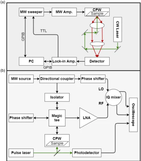
The setup of the ODMR spectrometer is shown inFigure 1. The CPW holding the sample is illuminated using a continuous wave laser (532 nm Coherent Verdi 5G frequency-doubled Nd:YAG).
The luminescent light is collected and focused by the so-called
“image relay”consisting of an achromatic doublet pair (Thorlabs MAP1030100-B) to a spectrograph (Horiba JY iHR320) equipped with a photomultiplier tube (Hamamatsu R2658P) and a single- pixel InGaAs detector (Horiba DSS-IGA010L). The former covers
Figure 1. a) Block diagram of the ODMR setup and b) theμ-PCD setup. Passive attenuators and DC blocks are not shown to retain clarity.
the ultraviolet (UV) to near infrared (NIR) range (185–1010 nm), whereas the latter is optimized for the NIR range (1000–1900 nm).
The detector output is connected to a lock-in amplifier (Stanford Research Systems, SR830) through a transimpedance amplifier.
The output of the microwave signal generator (HP83751B) is chopped by the TTL (transistor–transistor logic) signal coming from the lock-in amplifier. The microwaves are fed into an ampli- fier (Kuhne KuPa 270330-10A, Gain¼40 dB) and then sent to the CPW which has a 50Ω termination at its end. The CPW is placed on a two-axis miniature dovetail translation stage (Thorlabs DT12XY/M) during room temperature measurements.
To apply external magneticfield, the stage and the other optics parts are placed on a rail that can be rolled into the middle of an electromagnet with a magneticfield up to 1.2 T.
2.2. Theμ-PCD Spectrometer
Figure 1 shows the μ-PCD measurement setup which is a modification of our previous resonator-based, time resolved μ-PCD setup described elsewhere.[23] A Q-switch pulsed laser (527 nm Coherent Evolution-15, frequency-doubled Nd:YLF) with a 1 kHz repetition rate, pulse energy of 150μJ, and a pulse width of 1.7μs is used for excitation of charge carriers in the sample placed on the CPW.
The microwave oscillator (Kuhne MKU LO 8-13 PLL) serves as the source of the probing microwave (MW)field and as the local oscillator of a double-balanced in-phase quadrature (IQ) mixer.
The directional coupler sends half of the incoming power through an isolator (to avoid damage of the oscillator unit by reflected power) to the magic tee, and the other half drives the IQ mixer. Half of the incoming microwave power is directed toward the CPW, and the other half to the port with a phase- shifter and a variable attenuator attached. The waves reflected from the CPW and the other port interfere with each other on the fourth port allowing us to get rid off the DC reflection by setting the attenuation and phase properly. The previously described MW bridge is followed by a low-noise amplifier (JaniLab Inc. Gain¼15 dB) and the amplified signal is fed to the IQ mixer. The I (in-phase) and Q (quadrature) signals down- converted from the detected RF signal are digitized with an oscilloscope (Tektronix MDO-3024, BW¼200 MHz) which is triggered by the signal coming from the photodetector (Thorlabs DET36A/M) sensing the laser pulse.
2.3. The Cryostat
To conduct cryogenic measurement, we built a closed cylindrical compartment with optical access through a quartz window (∅100) and MW connection using an UHV SMA (ultra-high vacuum SubMiniature version A) connector. The CPW isfixed to a copper cube attached to the inner tube that can befilled with liquid nitrogen from the outside. The space between the two tubes where the CPW is placed is evacuated using a turbomolecular pump (Pfeiffer HiCube Eco). Vacuum level of 106mbar is easily achievable and grants long enough measurement time without any condensation problems on the outside or heating of the sample.
2.4. Samples
ODMR measurements were performed on single crystal (33 0.3 mm) type-Ib diamond samples (Element Six Ltd.) produced by high pressure high temperature method (HPHT), containing less than 200 ppm substitutional nitrogen. After neutron irradi- ation of the diamond plates in the Training Reactor of the Institute of Nuclear Techniques (located at the Budapest University of Technology and Economics) for 8 h at 100 kW power with a total fluence of 1017cm2 (31016cm2 in the 100 eV–1 MeV range), the samples were annealed under dynamic vacuum (105mbar) at 800–1000C to help the diffu- sion of vacancies creating the NV centers. To dissolve surface contamination, samples were put into vials containing a mixture of acetone and isopropyl alcohol and bath sonicated for 15 min.
μ-PCD measurements were conducted on phosphorus-doped silicon wafer with an approximate surface of 10 mm2and a thick- ness of 200μm. The resistivity of the sample was 0.528Ω⋅cm, as determined by a four-point sheet resistivity measurement technique.
3. Spectrometer Characterization
3.1. ODMR on NV Centers in Diamond
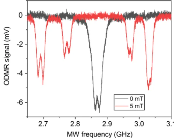
In this article, we present a range of measurements to demon- strate the versatile applicability of CPWs. First, ODMR measure- ments in variable external magnetic fields are shown along with a wavelength-resolved zerofield ODMR map. We conducted ODMR measurements on diamond samples to demonstrate the advantages of applying CPWs for MW irradiation. Figure 2 shows microwave frequency sweeps performed in zero magnetic field and also in 5 mT.
These spectra were acquired in a constant external magnetic field, whereas the microwave frequency was swept and chopped by the TTL signal of the lock-in amplifier.Figure 3on the other hand shows a magnetic field sweep at a constant microwave frequency of 9.2 GHz. Here, the MW amplifier was replaced with one working in the X-band (Kuhne KuPa 9001250-2A,
Figure 2. ODMR on NV centers in diamond detected at 680 nm. In zero magneticfield (black line), the resonances are degenerate, whereas apply- ing external magneticfield of 5 mT (red line) resolves the degeneracy.
Gain¼26 dB). This detection method is essentially the same as if it was a conventional electron spin resonance but the signal is detected optically. The principle of detection is that the micro- wavefield is frequency modulated using the lock-in amplifiers’ local oscillator as a sine source connected to the microwave oscillator. In Figure 3, the intensity of such ODMR signal is exam- ined as the amplitude of the modulating sine wave increases.
The modulation depth was set to 6 MHz V1 meaning a maximum deviation of 18 MHz in this measurement, however,
above 2 V, no significant increase in the ODMR amplitude can be seen.
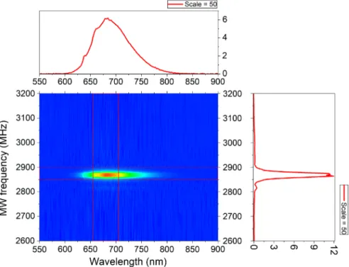
Figure 4shows individual ODMR spectra combined together to form a so-called ODMR map. This closely resembles emis- sion–excitation maps used in photoluminescence (PL), with the exception that one axis is the microwave frequency, whereas the other is the wavelength of the emitted light. This measure- ment was conducted in zero external magneticfield in the form of wavelength sweeps atfixed MW frequency. Here, the micro- wave sweeper is set to continuous-wave mode and wavelength- resolved PL is recorded as the grating of the spectrometer is rotated. In our setup, we simultaneously detect the DC voltage (the PL signal) and the AC component (the signal detected by the lock-in amplifier) which is the ODMR signal.
The measurement time is determined by the required resolution and range in wavelength and microwave frequency and the integration time. The map shown in Figure 4 was recorded with a 0.5 nm wavelength resolution and a 100 ms inte- gration time. The microwave frequency resolution is 2 MHz in the middle and was changed in bigger steps (10–50 MHz) moving away from the resonance resulting in 45 different values.
Altogether, this results in a measurement time of 52.5 min.
3.2.μ-PCD on Silicon Wafers
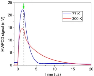
Figure 5shows theμ-PCD (or theμ-PCD signal) measured on a phosphorus-doped silicon sample at room temperature and at 77 K. The signal magnitude was obtained from the square root of the squared sum of the I and Q components. The CPW can be readily adapted to cryostat experiments as it can be conveniently
Figure 4. ODMR map. The upper panel is the wavelength-resolved microwave frequency averaged (taken in the range 2849–2899 MHz) PL similar to the well-known PL spectrum of NV centers. The right panel shows a vertical profile cross section (taken in the range 655–705 nm), which corresponds to the microwave frequency-resolved ODMR signal.
Figure 3. Frequency modulated and magnetic field swept ODMR measurement at 9.2 GHz on NV centers in diamond detected at 680 nm. Note that the derivative Lorentzian lineshapes are due to the frequency modulation similar to magnetic field modulation found in conventional electron spin resonance spectrometers.
placed on the coldfinger of an arbitrary cryostat. In contrast, a microwave resonator usually suffers from a change in the resonant frequency (and the quality factor) as a function of the temperature which affects the measurement sensitivity and also care is required to tune the source frequency to that of the resonator eigenfrequency. The CPW design is free from all these complications.
In case of time-resolved microwave detection, the use of microwave resonators is also impractical as the resonator bandwidth (typically, 100 kHz–1 MHz) significantly limits the available time resolution.[23]The typical power to microwavefield conversion is 2.171012T2W1 for a TE011 type cylindrical cavity. Following the calculations presented in the study by Simons and Arora[24]for our CPW with gaps of 250μm separated by 1400μm and a total width of 6 mm, this factor is 0.88 108T2W1. This means that the CPW performs as a cavity with a Q-factor of 4000.
As shown in Figure 5, the cooling leads to shortening of charge carrier lifetime in the investigated material. This is described by the Shockley–Read–Hall theory.[25]The impurities introduce empty gap states, thus giving a rise to recombination.
However, these levels can be occupied by thermally excited elec- trons. With decreasing temperature, fewer states are occupied therefore more recombination centers are present in the sample and the optically excited electrons have a shorter lifetime.
4. Conclusion
We presented the development of an ODMR spectrometer and a microwave photoconductivity decay measurement setup. Both instrument benefit from the CPW structure, namely, the easy optical access to the sample compared to classical microwave res- onators and the broadband operation. Low-temperatureμ-PCD measurements reveal decreasing carrier lifetime as the silicon sample is cooled. We pointed out that in specific cases, resona- tors can outperform CPWs in terms of accuracy and sensitivity,
but their advantage turns out to be a disadvantage when one needs to change measurement parameters such as microwave frequency or sample temperature. The fast μ-PCD setup can reveal information on charge carrier dynamics in intensively studied novel photovoltaic materials such as methylammonium halide perovskites.
Acknowledgements
This work was supported by the Hungarian National Research, Development and Innovation Office (NKFIH) grant nos. K119442 and 2017-1.2.1-NKP-2017-00001 and by the National Research, Development and Innovation Fund of the Hungarian Government grant no. NVKP_16-1- 2016-0018. The research reported in this paper and carried out at BME has been supported by the NRDI Fund (TKP2020 IES, grant no. BME-IE-NAT) based on the charter of bolster issued by the NRDI Office under the aus- pices of the Ministry for Innovation and Technology.
Conflict of Interest
The authors declare no conflict of interest.
Keywords
coplanar waveguides, microwave-detected photoconductivity decay, nitrogen-vacancy centers, optically detected magnetic resonance
Received: June 3, 2020 Revised: October 1, 2020 Published online: October 26, 2020
[1] M. C. Fischer, J. W. Wilson, F. E. Robles, W. S. Warren,Rev. Sci.
Instrum.2016,87, 031101.
[2] C. Lee, T. Rohwer, E. J. Sie, A. Zong, E. Baldini, J. Straquadine, P. Walmsley, D. Gardner, Y. S. Lee, I. R. Fisher, N. Gedik, Rev.
Sci. Instrum.2020,91, 043102.
[3] EPR of Free Radicals in Solids(Eds: A. Lund, M. Shiotani), Springer, Dordrecht2003.
[4] D. Stich, F. Späth, K. Hannes, A. Sperlich, V. Dyakonov, T. Hertel, Nat. Photonics2014,8, 139.
[5] P. A. Lane, L. S. Swanson, Q. X. Ni, J. Shinar, J. P. Engel, T. J. Barton, L. Jones,Phys. Rev. Lett.1992,68, 887.
[6] A. Gruber, A. Dräbenstedt, C. Tietz, L. Fleury, J. Wrachtrup, C. von Borczyskowski,Science1997,276, 2012.
[7] P. Neumann, R. Kolesov, V. Jacques, J. Beck, J. Tisler, A. Batalov, L. Rogers, N. B. Manson, G. Balasubramanian, F. Jelezko, J. Wrachtrup,New J. Phys.2009,11, 013017.
[8] W. Harneit, C. Meyer, A. Weidinger, D. Suter, J. Twamley,Phys. Status Solidi B2002,233, 453.
[9] J. Shinar,Laser Photonics Rev.2012,6, 767.
[10] J. Wrachtrup, C. von Borczyskowski, J. Bernard, M. Orrit, R. Brown, Phys. Rev. Lett.1993,71, 3565.
[11] M. Kunst, G. Beck,J. Appl. Phys.1986,60, 3558.
[12] B. Berger, N. Schüler, S. Anger, B. Gründig-Wendrock, J. R. Niklas, K. Dornich,Phys. Status Solidi A2011,208, 769.
[13] G. F. Novikov, A. A. Marinin, E. V. Rabenok,Instrum. Exp. Techn.2010, 53, 83.
[14] K. Sasaki, Y. Monnai, S. Saijo, R. Fujita, H. Watanabe, J. Ishi-Hayase, K. M. Itoh, E. Abe,Rev. Sci. Instrum.2016,87, 053904.
[15] C. P. Wen,IEEE Trans. Microw. Theory Tech.1969,17, 1087.
Figure 5.μ-PCD measurement conducted on phosphorus-doped silicon.
Red line shows the decay at room temperature and the blue spectrum was recorded at 77 K. The green arrow and the dashed line indicate the end of the laser pulse.
[16] W. Jia, Z. Shi, X. Qin, X. Rong, J. Du,Rev. Sci. Instrum.2018,89, 064705.
[17] S. B. Cohn,IEEE Trans. Microw. Theory Tech.1969,17, 768.
[18] R. Simons, Coplanar Waveguide Circuits, Components, and Systems, Wiley, New York2002.
[19] F. Gustrau,RF and Microwave Engineering, Wiley, Hoboken, NJ2012.
[20] S. Yamamoto, K. Shitamitsu, H. Kurisu, M. Matsuura, K. Oshiro, H. Mikami, S. Fujii,Phys. Status Solidi B2004,241, 1769.
[21] S. G. Cho, J. Kim, I. Kim, K. H. Kim, M. Yamaguchi,Phys. Status Solidi A2007,204, 4133.
[22] L. Yuan, Z. Yue, S. Meng, L. Li,Phys. Status Solidi A2014,211, 1828.
[23] B. Gyüre-Garami, B. Blum, O. Sági, A. Bojtor, S. Kollarics, G. Csősz, B. G. Márkus, J. Volk, F. Simon,J. Appl. Phys.2019,126, 235702.
[24] R. N. Simons, R. K. Arora,IEEE Trans. Microw. Theory Tech.1982,30, 1094.
[25] R. N. Hall,Phys. Rev.1952,87, 387.