Óbuda University
PhD Thesis
Investigation of optrodes for infrared stimulation in the deep tissue
HORVÁTH, Ágoston Csaba MSc electrical engineer
Supervisor: FEKETE, Zoltán PhD
Doctoral School on Materials Sciences and Technologies Head of the Doctoral School: RÉGER, Mihály, Dsc
Budapest, April 2020.
2
Contents
1 Preface ... 5
1.1 Motivation and goals ... 5
1.2 Structure of the dissertation ... 6
2 Introduction to neural microdevices ... 7
2.1 Biomedical MEMS and neuromodulation ... 7
2.2 Implantable microdevices with integrated optics ... 9
2.3 Optical stimulation methods... 13
2.4 Thermal stimulation... 16
3 Experimental ... 19
3.1 Design ... 19
3.2 Microfabrication... 22
3.2.1 Optical dummy samples... 23
3.2.2 IR optrodes ... 24
3.3 Packaging ... 26
3.4 Compliance with the requirements and constraints... 28
3.5 Electrochemical characterization ... 29
3.5.1 Electrochemical impedance spectroscopy ... 30
3.5.2 Electroplating ... 31
3.6 Optical characterization ... 33
3.6.1 Waveguide efficiency ... 35
3.6.2 Far field diffraction ... 37
3.6.3 Absolute power... 42
3.7 Thermal characterization ... 43
3.7.1 Calibration of integrated temperature sensor ... 43
3
3.7.2 In vitro testing of heat distribution... 47
3.8 In vivo validation of the functional optrode ... 48
3.8.1 Design of experiments ... 48
3.8.2 Measurement automation ... 50
3.8.3 Surgery ... 51
3.8.4 Stimulation protocols ... 52
3.8.5 Electrophysiology ... 52
4 Results ... 53
4.1 Evaluation of optrode technology through visual inspections ... 53
4.1.1 Thesis 1. ... 55
4.2 Electrochemical performance of recording sites ... 56
4.2.1 Improvement in site impedance ... 57
4.2.2 Soak tests ... 58
4.2.3 Thesis 2. ... 59
4.3 Optical performance of integrated waveguides ... 60
4.3.1 Relative beam power tests ... 60
4.3.2 Beam divergence tests ... 64
4.3.3 Comparison of relative and absolute power ... 65
4.3.4 Effect of fibre optic core and connector ... 66
4.3.5 Thesis 3. ... 69
4.4 Thermal properties of the devices ... 70
4.4.1 Calibration results of external temperature measurements ... 71
4.4.2 Integrated vs. external temperature ... 72
4.4.3 Spatial distribution of temperature... 73
4.4.4 Calibration of individual probes for in vivo tests ... 75
4
4.4.5 In vivo performance of temperature sensor ... 76
4.4.6 Thesis 4. ... 77
4.5 In vivo optical stimulation ... 77
4.5.1 Thesis 5. ... 86
5 Potential applications and benefits ... 87
6 Conclusion ... 88
7 Acknowledgement ... 89
8 References ... 91
9 Appendices ... 105
9.1 Comparison of phase plot of recording sites’ impedance before and after electroplating . 105 9.2 List of acronyms ... 105
5
1 Preface
1.1 Motivation and goals
The development of deep-brain implants that are simultaneously able to monitor neural activity and to stimulate the same tissue environment is advantageous to gain comprehensive information on the behaviour of cooperating neuronal population. Means of modulation of neuronal activity are acting through electrical [1], [2], [3], [4], [5], pharmacological [6], [7], [8], [9], [10] or optical intervention [11], [12], [13]. Among clinically relevant stimulation methods [1], [14], [15], photo stimulation is a promising tool, since electrical crosstalk effects, which contaminates recorded brain signals during electrical stimuli, are limited [16]. The most often used technical term for these devices, which can deliver light to neurons and can record evoked potentials, is optrode [17], [18].
A special field of optical neuromodulation applies infrared (IR) light for several beneficial reasons [19]. It is simple, as does not require any genetic transformation [20]; its longer wavelength provides superior penetration in tissues [21] and facilitates artefact-free recording of electrophysiological signals [22], [23]. During my PhD work, I developed a single-crystalline silicon-based, Michigan-type (in-plane) IR optrode capable for simultaneous deep-brain electrophysiological recording and temperature sensing (see Fig.1.). Although the discovery of IR-induced modulation of cellular activity dates back to the early 2000s, such an integrated, multimodal, long neural probe has never been created.
Thanks to this compact investigation tool, further knowledge about the interaction of IR light and deeper regions of the neural tissue can be extended in vivo in a minimally invasive way.
6
Figure 1: Concept of the multimodal optrode developed during my PhD work. [24]
1.2 Structure of the dissertation
At the beginning of my dissertation I give an overview of related fields in the literature of neural microdevices. I briefly introduce some neuroscientific aspects of the applications and the contemporary opportunities of the ri ch field of implantable neural microdevices with integrated optics. Then I sum up the mechanism of optical and thermal stimulation methods of the nervous system. I introduce the optrode devi ce through the description of its expected functionalities and the details of its design and fabrication process. All of the fulfilled test methods of the optrode’s functionalities are also introduced: benchtop tests of the device development, calibrations of individual products, functional tests in vitro and in vivo validation as well. I discuss the results in separate subchapters comparing to the literature, and my related theses are highlighted at the end of the chapters. Another separate chapter is devoted to the application opportunities and benefits related to the o ptrode in question. At the end of the dissertation there are the lists of the cited literature, my publications and appendices containing supplementary figure and data, and the explanation of the used acronyms.
7
2 Introduction to neural microdevices
Neural microdevices can be classified based on various aspects: e.g. human or animal purpose; central or peripheral nervous system is targeted; chronic or acute , cortical or deep- tissue application. They can provide sensing or stimulating functions or both. The final applications mentioned below require different approaches relying on the use of a wide variety of materials and structural layout. The following literature overview of implantable microdevices will focus on some of the relevant efforts from literature t hat are closely related to the topic of my PhD work.
2.1 Biomedical MEMS and neuromodulation
MEMS is the acronym of micro electro-mechanical systems. MEMS devices are manufactured using semiconductor technology, which is also used to produce integrated circuits. MEMS devices are often made of silicon (Si) or at least their fabrication process relies on silicon microtechnology. MEMS technology offers high precision, and therefore fine features in device layout due to advances in processes like photolithography, thin film deposition and etching [25], [26], [27], [28], [29]. Further advantage of such micromachining approach is that batch fabrication provides several devices with low variability in characteristics at relatively low unit c ost [28], [29]. Before the advent of MEMS in the biomedical field, several material and manufacturing process were proposed depending on the targeted surgical application . First deep-brain implants were made from metal wires (like tungsten or stainless steel) to monitor the extracellular electrical activity in neurophysiology experiments [30]. Since then, additional technologies have emer ged in this field, e.g. silicon-based microelectrodes [31], [32], [33] and polymer electrode arrays [34], [35]. The essential capability of these microimplants is the interrogation of neurons through tiny arrays of recording sites (e.g. circular, 15 µm diameter [36], [35] or 10×10 µm2 rectangular Au recording sites [33]). Brain functions have been researched for many decades and although amazing results have been achieved in many areas, a number of mechanisms inside this complex organ remained unclear. Neural signals that are usually recorded by the most commonly applied probes are interrogating a couple dozens of neurons, however there are billions of neurons in the brain. In order to get more detailed knowledge especially about more comprehensive, general brain functionalities and
8
correlations, larger number of individual neurons needs to be simultaneously monitored.
That is the reason why the combination of CMOS and MEMS technologies have been proposed to construct high-density electrode arrays [37], [38]. Beyond this important neurophysiological functionality, integrat ed modalities like drug delivery [39], [40], neurochemical sensing [41], [42] and optical stimulation [43], [44] are emerging extensions on such devices, which offer a novel toolset in the microscale investigation of cell ular process. Local drug delivery is used for example to treat a tumour [45], meningitis, ventriculitis, and central nervous system associated infections [46]. Neurochemical sensing focuses on the observation and investigation of neurotransmitters (e.g. dopamine) to gain useful information also for further treatments [41], [47], [48], [42]. Optical neuromodulation methods also represent an emerging technology, and will be introduced in more details in later chapters. Although not all of the followings can be integrated into needle-like microdevices, I briefly refer to additional neuromodulation techniques.
Electrical neuromodulation as a symptomatic treatment of Parkinson’s disease (PD), called deep brain stimulation (DBS), is a success story of the field. The technique relies on a stimulator probe implanted permanently into the brain tissue, and an external device, which delivers current pulses in a pre-defined sequence to terminate tremor [49]. The implanted electrodes of DBS devices cause a potential gradient across a neuron, which lead s to intracellular ionic current flow and localized depolarization and hyperpolarization of the cell membrane. This way, a region of cell membran e hyperpolarization is created, which is sufficient to block action potential propagation, thereby achieving ne ural inhibition.
Briefly, stimulation appears to block the signals that cause disabling motor symptoms, and so helps to provide greater control over movement. In case of transcranial magnetic stimulation (TMS) potential gradients are induced in the tissue by a rapidly changing strong magnetic field (>1 T). The design of a micro-TMS system has been recently reported which reduces the spatial resolution by an order of magnitude [50]. Nevertheless, the large power consumption is still a limitation not yet overcome by fully implantable stimulator. Several other experiments have indicated that temporally modulated ultrasound waves can elicit action potentials in brain cells [51]. Their method is called transcranial ultrasound stimulation. Up to now, very little is understood about mechanobiology of affected cells, although proposed mechanisms have included cavitation and thermal effects. Of course,
9
each approach has advantages and disadvantages, so to make a reasonable solution for a particular neuromodulation, one is facing with trade-off.
2.2 Implantable microdevices with integrated optics
In literature, the comprehensive name of implantable devices what can deliver light to neurons and electrically recording them is ‘optrode’ [17], [18]. Before optrodes have been introduced, bulky optical fibres implanted in the tissue were only used to stimulate neuronal population using light in spatially confined manner [52], [53], [54], [55]. The key advantage of optrodes is that they provide multiple functions in a single device, which helps to mitigate the extent of cellular damage otherwise induced using standalone recording and stimulation devices. Such multifunctional tool also provides precise relative location of recording and stimulation spots eliminating the complicated positioning of individual devices [56]. The state-of-the-art optrodes can be divided in two main groups:
passive and active optrodes (cf. Fig. 2. A-B and C-D, respectively). Passive optrodes contain a passive microoptical element, which delivers light coupled into the system from an external light source (optical fibre, waveguide). In active optrodes, light is generated through integrated sources (like microLEDs) located on the probe [57], [13], or even on its shaft [58], [59], [60]. In this chapter, technology of passive optrodes is briefly described using specific examples from the literature. Figure 2 depicts main constituent parts of optrode devices in schematics.
Figure 2: (a) Optical fibre (yellow) affixed to the substrate (grey) of the passive optrode.
(b) Optical fibre coupled to the surface waveguide (cyan) structure of the passive optrode.
(c) Integrated light source (black) coupled to the surface waveguide st ructure of the active optrode. (d) Light sources integrated on the penetrating shaft of the active optrode. Based on the Fig. 4. in [30].
The aim of the first approaches was to supplement conventional in-plane (Michigan-type) silicon microelectrodes with secondary waveguiding structures. Royer et al. com bined multiple-shank silicon probes with thinned optical fibres fixed on each shank [61]. Their
10
method incorporates standard glass optical fibres into the technology of planar silicon microelectrodes to form integrated waveguides on the probe shaft (see Figure 3 a&b). The inherent drawback of this technique was that the overall size of the implant was pretty bulky. To circumvent this, wet chemical (with KOH [62]) or dry (deep reactive ion etching – DRIE [63]) etching techniques were used to form a groove in the Si substrate to embed the fibre into the bulk (see Figure 3 c).
Figure 3: (a) Side and (b) front view images of electrode shanks with a glued optical fibre [61].
(c) Photograph of the fabricated Si optoneural probe tip with the optical fibre embedded in a probe shank [63].
Cho et al. used SU-8 polymer as the core of the integrated micro -waveguide on the top of the conventional passivation SiO2 layer on the microelectrode’s shaft (Figure 4 [64]). The advantages of this method were to downscale the waveguide dimensions and to provide a more accurate positioning with respect to the probe tip and to the recor ding sites.
Kobayashi et al. used silicon-nitride as the core of the integrated micro-waveguide similarly on the top of the SiO2 passivation layer [65], however, in this case, the top cladding was also a SiO2 layer, not only the surrounding air. Although, they applied thinner layers even for the core and for the cladding, the entire implant diameter was wider, because their probe was designed with a longer shaft, which required more robust substrate. Wu et al. chose silicon-oxynitride as core material instead of SU-8 polymer or SiN (Figure 5 [66]). They also applied SiO2 as cladding layer completely surrounding the core. All group realized the coupling between the light source and the integrated waveguide with butt - coupling of an optical fibre [64]–[66] or simply butt-coupled a laser diode right to the embedded fibre [62]. The precise positioning of the coupling fibre in the first cases was ensured by a DRIE-etched fibre guiding groove.
11
Figure 4: (a) SEM overview of the neural probe with optical fibre mounted at the end of the SU-8 waveguide. (b) Iridium electrode array around stimulation site. (c) Coupling between optical
fibre and waveguide [64]
Figure 5: (a) Relative size in contrast with a US quarter. (b) Microscope image of probe tip showing the electrode array and the SiON waveguide. (c) SEM image of the waveguide magnified
at the distal end. (d) SEM image of the waveguide at the proximal end and the optical fibre groove [66].
12
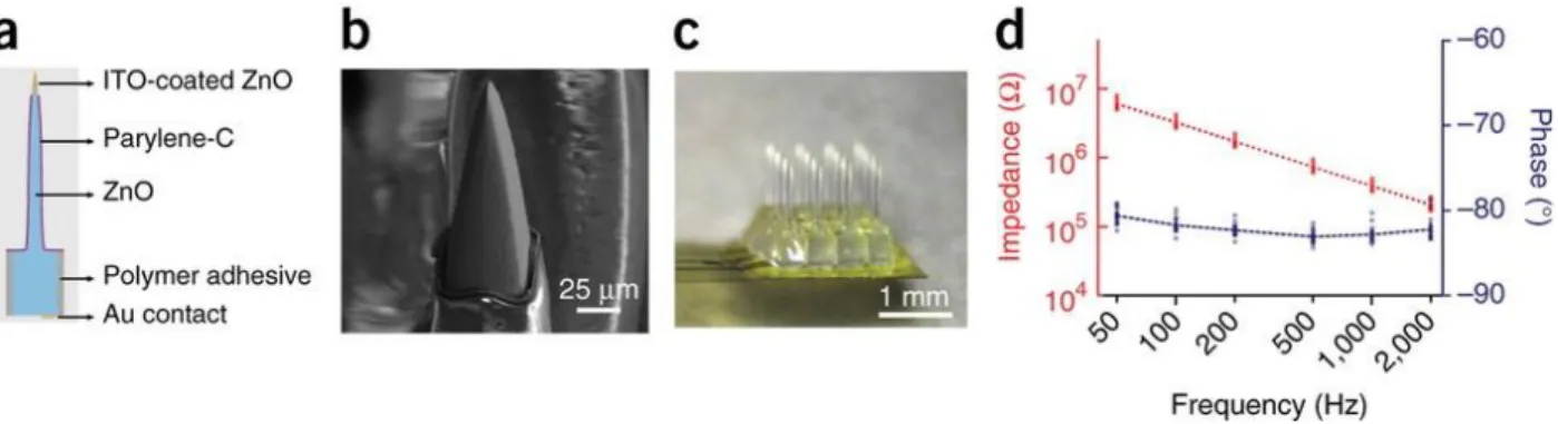
Lee’s and Abaya’s work present another approach: out-of-plane microprobe arrays [67], [68]. Lee et al. chose ZnO as the substrate material because of its physical proper ties, suitability for device microfabrication and biocompatibility. ZnO is transparent across the visible spectrum into the near-infrared range, nontoxic and biocompatible. They generated square pillar arrays by means of mechanical dicing. Later , they tapered these square pillars by a custom developed multistep chemical etching process. For electrical isolation, first they sawed trenches into the substrate and filled them with med ical-grade polymer adhesive, then each pillar was coated with Parylene C. The refractive indices of these two materials are nZnO ≈ 2.0 and nParylene ≈ 1.6. To form electrical contact to the brain tissue, they removed the Parylene C to expose the tips of the optoelectrodes, then finally they sputtered a thin transparent conductive layer of indium-tin-oxide (see Fig. 6.). This device is able to perform simultaneous light delivery and electrical readout thanks to the optically transparent and electrically highly conducting semiconductor behaviour of the ZnO crys tal.
Note, that this waveguide optrode array is used for optogenetic application with a 473 nm blue laser.
Figure 6: Transparent, electrically conductive ZnO micro-optoelectrode array (MOA device) for multichannel intracortical neural recording and optical stimulation. (a) A single optoelectrode
structure. The ZnO shank is electrically isolated by Parylene -C except for the active tip area, and shanks are isolated from each other by polymer adhesive. (b) Electron microscope image of
the microscopically smooth tip with the recording area, covered by a final ITO conducting overlayer. (c) A 4 × 4 MOA device flip-chip bonded on thin, flexible and semitransparent polyimide electrical cable. (d) Electrical impedance spectroscopy of MOAs (n = 18) with
uniform impedance across the arrays. [67]
Abaya et al. took advantage of the experience gathered during the development of the Utah Slant Electrode Array (USEA). They tapered the pre -sawed silicon pillars with wafer-scale wet chemical etching in a 1:19 acid mixture of HF (49%) and HNO3 (69%). They also
13
realized the coupling between the light source and each waveguiding silicon cone with butt-coupling of an optical fibre. In most cases, refractive index matching material is also used between the fibre’s end and the polished (flat) backside of the silicon array. Note, that this device is the first written development of an optrode array made for deep brain infrared neural stimulation (INS), however, their system is only a technological demonstration, and was never applied in living tissue.
Figure 7: SEM images of a Utah Slant Optrode Array. The array is bulk-micromachined from intrinsic (100) silicon. (a) Optrode lengths vary from 0.5 to 1.5 mm. (b) Taper profile of the shortest optrode. (c) Definition of optrode sections along the path of light propagation: 500 µm
backplane, base extending 120 µm into linearly tapered shank, and ∼50 µm tip. [68]
2.3 Optical stimulation methods
Typically, optrode devices are used for optogenetic applications (see Fig . 8.). This method incorporates genetic modification of specified neurons making them sensitive to certain coloured (visible) light radiation [18]. The popular set of wavelength used in optogenetic applications: 405 nm [44] or 473 nm [52], [61], [69] (blue), 561 nm [61] (yellow-green) or 635 nm [44] (red).
14
Figure 8: Illustration of the optogenetic technique using a blue light, which activates ChR2- expressing neuron cells by opening light sensitive ion channels [18].
Generally, optogenetics integrates light-sensitive proteins (opsins) into the cell membrane of specific cell types to form light-sensitive ion channels that can modulate action potential generation. Controlled operation of specific ion channels can be realized by illumination with a suitable coloured light depending on the opsin’s type. Simply, one can ‘switch’ on and off specified neurons by specified light. The main advantages of this method are its temporal and spatial precision: it is a fast, local and selective investigation tool in cellular level. However, its application in human targets is still challenging. However, there are ethical concerns because of the risks of genetical modification, there are few pioneering research of translational aims. There is an active clinical study on optogenetic vision restoration (NCT02556736) in the USA. Besides ethical issues, optogenetics entails the disadvantage of complexity of an additional time consuming and expensive procedure using genetic tools. Optogenetics has also another disadvantageous property: the typically used visible wavelength light causes artefact (noise) in the recorded neurophysiological signals [69]. It is originated from the photoelectric effect (Becquerel effect), when photons of a suitable frequency light eject an electron from a metal by strik ing it. The presence and movement of these generated electrons are similarly detected as electrical signal
15
superimposed on the electrophysiological recording. Alexandre Edmond Becquerel was who first observed the phenomenon in 1839, but Albert Einstein was who explained it in 1905. When light of a particular frequency strikes a metal surface, electrons are ejected. In that case, increasing the intensity only increases the number of electrons ejected . If the frequency is increased, the ejected electrons will travel faster. This is described by the equation:
𝐸 = ℎ ∙ 𝜈 ≥ ℎ ∙ 𝜈0 = 𝛷 (1)
where E is the energy of the incident photon, h is Planck constant, ν is frequency of the light, ν0 is the light frequency threshold necessary to generate photocurrents and Φ is the photoelectric work function. For most biomedical applications and neural technologies, frequency (ν) and wavelength (λ) can be equated through the formula ν = c/λ, where c is the speed of light. [70].
A special method, exploiting the produced light-sensitivity of neurons, is a widespread example of the application field known as two-photon imaging. The method is based on a quantum mechanical phenomenon: the energy of the light-matter interaction required for excitation can be obtained not only from a single photon, but also from two photons absorbed at the same time, each having half (or even less) of the energy required [71]. In case of multi-photon events, equation (1) can be rewritten as:
𝐸𝑁 = (𝑁 + 𝑆) ∙ ℎ ∙ 𝜈 (2)
where N is the number of photons colliding with the electron at the same time and S is a positive integer [72]. For example, 11 Hz two-photon raster scanning with a 30 mW, 920 nm laser increased the spiking activity of soma-targeted ChR2-expressing neurons in the mouse neocortex in vivo [73].
Another optical method, that does not need any genetical modification induces change in the thermal conditions in the tissue to modulate neurons [74]. This method uses longer wavelength light in the infrared regime (1400–2100 nm). Its one advantage is that the use of longer wavelength reduces the possibility of photoelectric effect [70]. Another key advantage is that IR stimulation does not require any genetic modification [20]. High
16
energy (0.3–0.4 J/cm2 at 1.87 and 2.1 µm [75]) IR light pulses (micro- to milliseconds) generate temperature transients (spatial and temporal) in neurons depolarizing their cell membrane and making them firing action potential [20]. Besides, the application of IR light in neural subjects has further capabilities: lower energy IR illumination was described as a mean of neural inhibition. Its background is summarized in next chapter.
2.4 Thermal stimulation
Infrared neural stimulation was initially achieved through the generation of spatial and temporal gradient in tissue temperature, which required high energy, custom designed lasers with low repetition rate. Later, it was discovered that low energy (0.050±0.012 J/cm2 [76]) irradiation can be also efficiently used. The effect of lower energy IR light is different than that of the high energy IR pulses. It is proved that IR illumination with lower radiant exposure than applied for stimulation caused reversible inhibition of action potentials, both their propagation and their generation [77]. Its mechanism is supposed as an effect of elevated background temperature [78]. The non-uniform rate increases in temperature- dependent Hodgkin-Huxley gating mechanism is the hypothesis proposed recently [79]
suggesting that higher temperature activates the voltage -dependent K+ channels faster, resulting sufficiently greater hyperpolarizing current to overcome depolarization [80].
Another experiment proves that the thermal sensitivity of certain ion channels of neurons (TRPV4) plays a fundamental role in stimulating effect of IR illumination [81]. Although, the ion channels from the TRP family of cation channels are expressed in almost every tissue and cell type [82], another method, called thermogenetics, also plans transgenic application of foreign temperature-sensitive ion channels for controlling neurons’
behaviour. Despite the promising results already reported in Drosophila [83], in mouse [84]
and in zebrafish [85], thermogenetics is still in its infancy. There is already a limited variety of ion channels suitable for application, especially in mammalian targets [85]. Besides the already mentioned disadvantage of genetic modification, thermogenetics is suitable in view of invasiveness of the stimulating method: as visible light required for optogenetics has to be delivered through a transcranial waveguide element, thermal “signals” can be delivered in a non-invasive way through external stimulus. Its simplest way is ambient warming which is lacking cell specific selectivity. Through the application of magnetic nanoparticles [86] what well absorb microwave/radiofrequency radiation, the spatial resolution of the
17
externally forced local tissue heating can be improved. The main disadvantages of these types of thermal stimulation methods are their temporal resolution and power consumption.
IR illumination is still promising, because rapid heating can be achieved and its penetration depth in tissues is more favourable than visible light’s one [21], [87]. Although penetration depth of light is strongly wavelength-dependent [88] and also depending on the examined tissue, effective deep-brain application of IR light still needs penetrating waveguides (cf.
Fig. 9.).
Figure 9: Potential applications of near infrared (NIr) illumination in Alzheimer’s and Parkinson’s patients. Cortical layers can be reached extracranially, deep regions require
intracranial devices. [89]
Since we discussed above heat induced neuromodulation techniques, we should not miss to mention thermal issues of the introduced optical methods. It was already mentioned above in this section that IR irradiation is purposefully applied for elevating the background temperature of the target tissue to achieve neuromodulation effect [76], [90], [91]. In cases where IR light is used for multi-photon excitation or imaging, so not for the purpose of heating, IR irradiation still has heating effect : in a study, where 920 nm CW
18
(continuous wave) illumination was probed, a ~1.8 °C/100 mW peak temperature increase was experienced [92]. Similarly, optical neuromodulation techniques that use visible light also have a thermal effect on the irradiated volume. A ΔT = 2 °C general limit is defined for the temperature rise of the outer surface of an implanted (medical) device with respect to the surrounding body temperature of 37 °C (cf. ISO 14708-1 standard). To meet this requirement, Schwaerzle et al. operated the red light-emitting (650 nm) integrated laser diode of their two-shank Si implant in pulsed mode. During a 25 s long 35 mA laser drive with a 100 kHz pulsing (duty cycle = 5%) the maximum temperature rise was 1 °C [57].
For the same purpose, Wang et al. also tested the driving parameters of the blue light- emitting (445 nm) laser diode integrated in their neuro-implantable device. They stated that the temperature rise increased with duty cycle and its upper limit is 10% when the driving current and the frequency are 100 mA and 10 Hz, respectively [13]. Although a standard acceptable heating limit has been set, brain researchers dealing with optical radiation of the tissue should also consider whether the effects induced / observed are indeed (only) a consequence of photosensitivity or perhaps a rise in temperature or the co mbined effect of the two.
19
3 Experimental
3.1 Design
The aim of the present device development was to create an implantable optical stimulation device, which is able to deliver IR light through its embedded bulk waveguide and holds sensors, which monitor the optically evoked electrical and thermal response o f the irradiated tissue. Device concept is shown in Figure 10. IR light is coupled from an optical fibre positioned close to a cylindrical coupling lens integrated in the optrode chip. After coupling, IR light is propagating through total internal reflection inside the probe shaft and exits the shaft at the end facet. The absorbed light is converted to heat, and the evoked change in cellular activity and tissue temperature is recorded through integrated sensors.
Since this goal requires a complex approach in view of microtechnology, I first addressed this issue by testing individual functionalities in two particular dummy structures.
Electrical recording sites and temperature sensors without optical functionality was realized and will be referred to as thermoelectrode [93]. The waveguiding modality of the device concept was first tested using optical dummy samples, where the silicon substrate
Figure 10: Schematic of the multimodal IR neural microsystem. Marked components: 1: Si substrate, 2: multimode optical fibre, 3: cylindrical coupling lens, 4: shaft with multiple functionalities, 5: probe tip. Figure is not to scale. ΔSR and ΔR m ean that optically induced temperature elevation changes the detectable spike rate of the affected neurons and the ohmic
resistance of the integrated temperature sensor. [95]
20
itself is used not only as the mechanical carrier, but also as an infrared waveguide thanks to special wet etching process developed by group members in a prior work [94].
To test the waveguide efficiency of the optrode two types of dummy samples were fabricated. Bare silicon chips without any thin film layer on top and with a 200 nm thick silicon-nitride layer on one (top) side. This pair of sample enables the investigation of the effect of the passivating layer on waveguiding efficiency, since prior work was only limited to Si optrode chips without dielectric thin films. Relevant parameters of the dummy chips are shown on Figure 11 A&B:
Figure 11: Schematics of optrode chip designs. A) Contour of optical dummy chip with coupling lens. B) Design of coupling lens. C) Contour of functional optrode chip with coupling lens and funnel-shape extension of fibre guide groove. All geometric dimensions are the same as in case
of optical dummies (A), but only with thinner shaft (170 µm). D) Design of funnel-shape extension of fibre guide groove’s inlet. All marked geometric dimensions are in [µm].
Based on the experiences and results I composed these aforementioned devices into one multimodal microsystem. The contour of optical dummy samples (Figure 11 A) and functional optrode chips (Figure 11 C) is the same. Both have a quadratic backbone and an elongated shaft. The backbone part will hold the bonding pads ensuring further connection of measuring wires and it incorporates a linear groove with a cylindrical lens ending (Figure
21
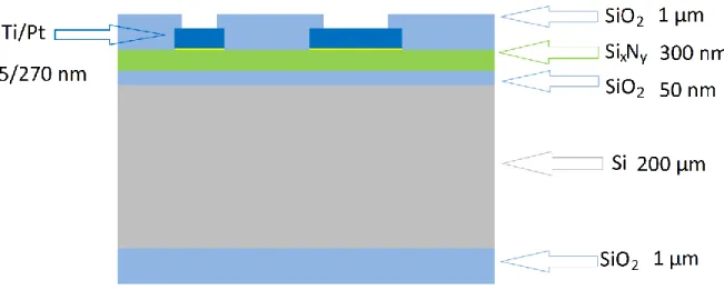
11 B). This groove is for embracing the optical fibre which delivers IR light from the source. The cylindrical lens ending is intended to support good efficiency light coupling from optical fibre to Si waveguide: two fenders help keeping the proper distance between the end facet of optical fibre and the front of the lens which focuses the incident light beams to the shaft. Functional optrode chip version’s layout is supplemented with a funn el shape (Figure 11 D) at the beginning of the fibre guide groove: it makes optical fibre insertion easier in practice. Unlike optical dummy samples, on the top side of functional chips there is not only a SiN layer (as in certain cases), but a sputtered platinum (Pt) thin-film packaged within a dielectric layer structure of silicon-dioxide and silicon-nitride (see Fig. 12.). The electrophysiological recording sites are formed as 30×30 µm2 Pt squares placed nearby the tip of the shaft, at a distance of 100 or 300 µm from each other. The thermal sensor, which is a meander-shape Pt wire on the same layer, is placed as close as possible to the recording sites ensuring true local thermal information during experiments (see Figure 13 & 33).
Figure 12: Cross sectional schematic of a functional optrode chip showing the layer structure with corresponding thicknesses (cf. Fig. 15.). Image is not to scale. [96]
The blunt tip of above design is advantageous regarding the optical characterization of the device, as the relevant optical information comes from a single plane and makes preliminary measurements easier to implement. Obviously, the penetration of the final device into the tissue is easier and induces less tissue damage if sharp tip design is applied, but in my initial experiments this particular shape was sufficient to test all functionalities in a reproducible manner either before or during in vivo application.
22
Figure 13: Schematic of the design of functional chip with magnified view of the tip. All marked geometric dimensions are in [µm].
3.2 Microfabrication
In the following section, the process steps of engineering three particular samples will be describe: dummy samples that do not hold any other functionalities on top of light delivery;
thermoelectrodes that hold all integrated functionalities except for light delivery; fully functional optrodes capable of light delivery, electric and thermal recording. However, each approach contains some similarities in certain phases of technology, I explain all details at each device configuration to give a comprehensive information, which helps to understand the underlying procedures of microfabrication. Si MEMS technology was chosen since it has been developed and improved for decades. Besides its many advantages, it may have inherent properties, that are not so beneficial for device fabrication. F or instance, the sidewalls of out of plane structure are difficult to fine -tune. To overcome this drawback, wet chemical methods provide additional freedom to polish these surfaces. That is why I complemented the fabrication sequences going to be described in the followings with further wet chemical steps.
23
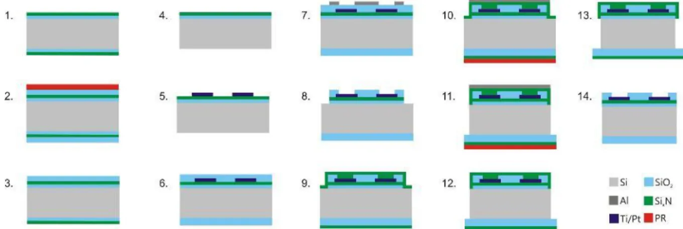
3.2.1 Optical dummy samples
The initial substrate was a 200 µm thick single-crystalline silicon wafer. Double-side polished wafers were used to maximize the efficiency of the integrated Si waveguide by maintaining the atomic smoothness of the wafer surface. A 200 nm thick low-stress silicon nitride (SiNx) film was deposited in an LPCVD chamber (Tempress Systems, Inc., Netherlands) at 830 °C and 200 mTorr. This single layer was chosen to anticipate the effect of the further functional layer structure on IR waveguiding. The gas flow rate of H2SiCl2
and NH3 was 160 sccm and 20 sccm, respectively. Residual contaminants were removed in a rinser dryer. Then a 400 nm thick APCVD oxide (SiO2) layer was deposited as a masking layer of further patterning of the nitride. After a 30 min annealing, the oxide was patterned by photolithography on the front side to open windows for nitride etching. After the etching of SiO2 by diluted HF, the photoresist (PR) was removed in aceto ne bath (step 1 in Fig.
14.).
Figure 14: Micromachining steps of optical dummy samples. (1) SixN deposition, CVD SiO2
masking SixN patterning; (2) Nitride etching; (3) Al mask photolithography for DRIE;
(4) Through-wafer DRIE forms the chip’s contour and the fibre guide groove; (5) Removal of Al and PR layers; (6) Wet chemical polishing. (7*) Optional nitride etching. Top-side nitride-
covered dummies made by applying steps (1)–(6). Bare Si optical dummy samples made by applying steps (1)–(7*).
The non-masked nitride surfaces were removed by wet etching in phosphoric acid, then the SiO2 mask was also removed (step 2 in Fig. 14.). Wet etching was used in both cases of oxide and nitride etching instead of dry etching to maintain the smoothness of the backside surface of the Si wafer, because wet etching removes materials selectively while dry etching is less selective and its mechanism of action includes physical ‘bombing’ of accelerated ions which does not respect material boundaries. A 300 nm electron-beam evaporated Al layer and additional PR cover (1.8 and 4.5 µm on front and backside,
24
respectively) were used as hard mask and etch stop of the electrode-shape release technique, the dry etching, using Bosch recipe in an Oxford Plasmalab System 100 DRIE chamber (Oxford Instruments Plc, UK). Chamber pressure was 30 mTorr, inductively coupled plasma power (ICP) was set to 750 W, C4F8 and SF6 flow rate were 100 sccm and 150 sccm, respectively. The duration of etch and passivation cycles were 4 and 9 s, respectively (step 3-4 in Fig. 14.). Finally, masking layers were removed in acetone and in nitric acid (step 5 in Fig. 14.). Fluorocarbon polymer inherently deposited on the trench sidewall during Bosch-process was removed in a high-temperature oven at 600 °C in O2. The planarization of the probe sidewall was achieved by immersing the wafer in a polishing mixture of HF : HNO3 : H3PO4 in a ratio of 1 : 8 : 1 at 20 °C for 2 min 40 s (etch rate: 9- 10 µm/min) (step 6 in Fig. 14.). This microfabrication process was supplemented with another nitride etching in phosphoric acid, only in case of bare Si samples (step 7* in Fig.
14.).
3.2.2 IR optrodes
The initial substrate was a 200 µm thick p-type (100) single-crystalline silicon wafer.
Double-side polished wafers were used to maximize the efficiency of the integrated Si waveguide by maintaining the atomic smoothness of the wafer front- and backside surface.
Wet oxidation of silicon wafers was performed at 1100 °C. 50 nm thick thermal SiO2 layer was grown on the substrate surface. To further isolate the recording sites from the bulk Si, a 300 nm thick low-stress silicon nitride (SiNx) film was deposited in an LPCVD chamber (Tempress Systems, Inc., Netherlands) at 830 °C and 200 mTorr (step 1 in Fig. 15.). The gas flow rate of H2SiCl2 and NH3 was 160 sccm and 20 sccm, respectively. The SiNx and SiO2 were removed from the backside of the wafer by wet etching in phosphoric acid and diluted HF, while front side layers were protected by low temperature oxide and SPR 4.0 photoresist (step 2–4 in Fig. 15.). Wet etching was used instead of dry etching to maintain the smoothness of the backside surface. A sacrificial Al layer was used to define the pattern of the TiOx/Pt recording sites, temperature monitoring filament and wires via a standard lift-off process (step 5 in Fig. 15.). First, a 300 nm thick sacrificial Al layer was deposited by electron beam evaporation. This was followed by the first photolithography step using Microposit 1818 photoresist (Rohm and Haas Company, USA), and etching steps defining the inverse pattern of the conductive layers. The conductive layers consisted of a 15 nm
25
thick adhesion layer of TiOx formed by reactive sputtering of Ti in an Ar/O2 atmosphere (Ar/O2 ratio was 80 : 20). 270 nm thick Pt was sputtered on top of TiOx. The deposition of the two layers was performed in a single vacuum cycle using a DC Magnetron sputtering equipment (Leybold GmbH, Germany). To complete the lift-off process step, photoresist and Al were removed in acetone and in nitric acid, respectively. In the next fabrication step, the top passivation layer of 1000 nm thick SiO2 layer was deposited using LPCVD at 430 °C in a gas mixture of SiH4 and O2 (step 6 in Fig. 15.). Contact and bonding sites were exposed by additional photolithography (Microposit 1818 photoresist) and dry etching step through a 100 nm thick aluminium hard mask (step 7 in Fig. 15.). Dry etching of the SiO2/SiNx/SiO2 dielectric stack was performed in an Oxford Plasmalab 100 DRIE chamber using fluorine chemistry (step 8 in Fig. 15.). 200 nm SiNx as a masking layer for wet chemical polishing was deposited again in the LPCVD system using the above parameters (step 9 in Fig. 15.). The probes were then micromachined by dry etching using Bosch recipe in an Oxford Plasmalab System 100 DRIE chamber (Oxford Instruments Plc, UK). Masking layer was e--beam evaporated aluminium on the front side, while bottom SiO2/SiNx stack acted as etch stop layer. A protective 4 µm thick photoresist layer was also utilized on the backside of the wafer (step 10–11 in Fig. 15.). Chamber pressure was 30 mTorr. ICP power was set to 750 W, C4F8 and SF6 flow rate were 100 sccm and 150 sccm, respectively. The duration of etch and passivation cycles were 4 and 9 s, respectively. Finally, masking layers were removed in acetone and in nitric acid (step 12 in Fig. 15.). Fluorocarbon polymer inherently deposited on the trench sidewall during Bosch-process was removed in a high- temperature oven at 600 °C in O2. The planarization of the probe sidewall was achieved by immersing the wafer in a polishing mixture of HF : HNO3 : H3PO4 in a ratio of 1 : 8 : 1 at 20 °C for 2.5 min (etch rate: 9-10 µm/min) (step 13 in Fig. 15.). The low-temperature oxide membrane at the bottom of the trenches was dissolved in buffered oxide etchant, then top and bottom SiNx protective layer was also removed completely in phosphor ic acid (step 14 in Fig. 15.).
26
Figure 15: Fabrication sequence of fully functional optrodes. (1) SiO2 and SiN deposition, (2) LTO deposition and front-side photoresist protection, (3) HF etch and PR remova l, (4) Backside nitride and oxide removal, (5) Ti/Pt deposition and lift -off, (6) LTO deposition, (7) Deposition, photolithography and etching of Al mask for DRIE, (8) Dielectric stack removal
in DRIE and Al removal in wet etchant, (9) SiN deposition, (10) Deposition, photolithography and etching of Al mask for DRIE with backside PR protective layer, (11) Deep silicon etching in
DRIE, (12) Removal of Al mask and protective PR layer, (13) Wet chemical polishin g, (14) HF etch and SiN removal in phosphoric aci d. [24], [97]suppl.
3.3 Packaging
After the microfabrication process, individual optrode chips were packaged to make optical and electrical connections to external light sou rces for stimulation and to amplifiers for neuronal recording and temperature monitoring on a custom -designed PCB, manufactured by Solutions System Ltd. First, in the middle line of the PCB a 400 µm deep trench was milled (step 2 in Fig. 16.). The aim of this trench is to bridge the height difference between the middle axis of the silicon chip and that of the optical fibre. This trench also helps to position the core of the stripped optical fibre into the guiding groove of the chip in a well- aligned fashion. The Si chip was then fixed with a double-sided adhesive tape (step 3 in Fig. 16.). It makes wire bonding and later the precise fibre positioning easier. Connection between the electrode bonding pads and the PCB leads was made using ultrasonic wire bonding (Kulicke-Soffa Industries, Inc., Singapore) utilizing 25 μm thick gold microwires (step 4 in Fig. 16.). The properly stripped and polished fibre was inserted into the chip’s groove (step 5 in Fig. 16.). In the groove, the fibre facet was fixed with index-matching glue (n = 1.56; Norland Products Inc., Cranbury, NJ, USA) which, in addition, helps to prevent contamination of the coupling area (step 6 in Fig. 16.) and improves the overall waveguiding efficiency. After UV light cure of the optical adhesive (25 min) the PCB was
27
mounted with PreciDip connector (Preci-dip SA, Switzerland) for providing electrical connection to external amplifiers to be used during electrochemical impedance spectroscopy tests and in vivo experiments. This through-hole socket also helps to keep the fibre along the PCB in a fixed position, and also reduces the sensitivity of the fibre to external mechanical impacts during surgery. Remaining gaps and connection points are filled with Araldite® 2014 adhesive (Huntsman Advanced Materials, Switzerland) to increase mechanical strength of the device (step 7 in Fig. 16.).
Figure 16: Main steps of IR optrode assembly.
As it was mentioned above, the selected optical fibre must be prepared properly preceding the assembly. First, the fibre is cleaved to the desired length. Then, most importantly, we must polish the fibre’s end facet to create a perfect light emitting surface. Another task is to strip the fibre’s furcation tubing and inner tube (protective polymer coatings around the fibre) to provide sufficient amount of stripped fibre protrusion for the insertion into the groove of the chip. During the project related to the device development, I tested three different optical fibre types. All of them was multimode optical fibre (NA = 0.22). I started working with one mounted with an LC connector, with 50 µm core and about 120 µm overall diameter (NewNetwork Ltd., Hungary). This connector type was found too prone to wobble what adversely affected the waveguiding measurements . So, I changed it with
28
another one mounted with an ST connector, with the same core/cladding ratio and diameter (FibreFab Ltd., UK). Later, I changed it with a fibre type with a wider, 105 µm core and about 125 µm overall diameter mounted with an SMA connector (Thorlabs Inc., USA).
These latter types of fibre have a wider furcation tubing to bear the heavier bayonet style (ST) or screw-type (SMA) connector. To avoid an unintended crack of optical fibres, the electrical socket was inserted in a distance of two pins (raster: 1.27 mm) from the edge of the PCB. Thanks to this additional surface, the furcation tubes can be adhered directly to the surface of the PCB and to the orthogonal side of the socket (step 9 in Fig. 16.). This robust fixing helps to avoid the bending of the fibres around a too short radius. Because of the mentioned positioning of the socket, the microwire bonding also had to follow the modification of the pinout (cf. step 4 in Fig. 16.). During the application of the first run of optrode chips, I noticed that depending on the etch time of wet chemical polishing of the chip’s sidewall, not all the optical fibres fitted to the guiding groove of the chip perfectly.
To circumvent this issue, I thinned the cladding of the fibres to the desired diameter before polishing their end facet. Using 50±1% buffered HF at room temperature (21–21.9 °C), I determined the etch of the cladding material, and performed the thinning of the cladding, if demanded. Relevant etch rates were 3.1 µm/min for FibreFab OM3 fibres, and 4.4 µm/min for Thorlabs M15 fibres. Because this HF etching not only thinned the cladding, but etched a bit the core material as well, it had to precede the abovementioned essential polishing of the fibre’s end facet.
3.4 Compliance with the requirements and constraints
• Acute in vivo functional test of the optrode device in rat somatosensory cortex and hippocampus: shaft length = 5 mm
• Easy pre-calibration of individual modalities (waveguid ing, temperature sensing, neural recording)
o Optical aspects
▪ Symmetry: square waveguide cross section
▪ Acceptable efficiency
• Smooth sidewalls: double-side polished wafer + wet chemical polishing
29
• A lens focusing the light emitted from the fibre on the waveguiding shaft
▪ Easy optical characterization → single emitted beam → blunt tip o Thermal aspects
▪ Local temperature measurement
▪ Simple, but robust construction
→ Single resistance thermometer as close to the tip as possible o Aspects of neural recording
▪ Small dimensions
▪ Multi-channel recording capability
→ 4 rectangular recording sites as close as possible to the tip, made of the same material as the integrated thermometer, within the same technological layer
▪ Reduction of signal-to-noise ratio: reduction of the impedance of the recording sites
• Reasonable minimization of the cost of all constituents at this early stage of research o Si wafer: double-side polished, sufficiently thin (not too thick), available in the market by default → 3”, p-type, 200 µm thick, double-side polished wafers with <100> crystallographic orientation, produced by the Czochralski method
o Connectors and sockets for measurement wirings: not too small for frequent manual handling, not too large for in vivo use, available in the market by default: PreciDip
o Optical fibre: not too thick / thin, not too fragile, multimode, available in the market by default → with different connectors: 1.: LC, 2.: ST, 3.: SMA 3.5 Electrochemical characterization
Before in vivo investigations, it is essential to analyse the electrical performance of devices.
On one hand, the long-term integrity of the layer structures should be tested i n wet environment. This is usually referred as soaking test in the literature. On the other hand, the characteristic property of the recording sites is investigated using Bode plots recorded
30
in the frequency range relevant to applications in the brain tiss ue (1 Hz – 10 000 Hz) [98]:
the typical range of local field potential (LFP) is 1–300 Hz [99], while spikes (often referred as single or multiunit activity (SUA/MUA)) are detected at higher frequencies between 300–10 000 Hz. Electrochemical impedance spectroscopy is a popular tool to provide information in this respect [100], [101], [102].
3.5.1 Electrochemical impedance spectroscopy
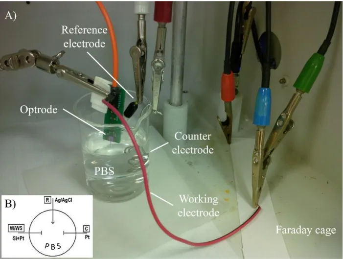
Electrochemical impedance spectroscopy (EIS) method uses a three-electrode cell. The schematic and a photo of the arrangement can be seen in Fig. 17.B&A, respectively. When voltage is applied between the reference (R) electrode (maintained at a constant potential) and the so-called working electrode (W/WS), it generates charge transport (electric current) between the W/WS and the so-called counter (C) electrode, and EIS measurement computes impedance values using these two measures, the present voltage and current.
After the immersion of an electrode in an electrolyte, the arrangement seems electroneutral, because the immediately occurred chemical reactions quickly reaches a steady state equilibrium. EIS method slightly moves away the arrangement from this equilibrium because of an applied AC excitation. The aim of it is that the expected ion and solvent transport from the electrolyte to the conductive film is not significant, so the morphological and electrochemical transformation of the film is negligible. Common evaluation of EIS is finding the lumped-parameter equivalent circuit model of the observed setup [103], [104], [105]. Another practice refers the hole characteristic with one measure, the amplitude value of the impedance at 1 kHz [106], [107].
31
Figure 17: (A) Photo and (B) schematic of 3-electrode setup for electrochemical inspection of recording sites.
In the lab of the Institute of Technical Physics & Material Sciences, Centre for Energy Research (EK MFA) I used a Gamry Reference 600 potentiostat (Gamry Instruments, PA, USA). The applied electrolyte medium of my experiments made in a Faraday cage was phosphate buffered saline (PBS; 0.01 M). The reference electrode was a leakless Ag/AgCl (3.4 mol/L KCl) electrode, the counter electrode was a Pt wire and each of the Pt electrophysiological recording sites was connected as a working electrode. Gamry Framework 6.02 software was used for automated control of measurement and recording, and Gamry Echem Analyst 6.02 was used for data evaluation. The applied AC voltage was 25 mVRMS, the frequency range was set between 1 Hz to 10 kHz.
3.5.2 Electroplating
Just before in vivo application, the impedance of the electrophysiological recording sites was reduced by electroplating porous Pt (or sometimes referred as black -Pt). This
32
additional porous layer on the top of the Pt recording s ites increases their specific surface area. The aim of it is to improve the SNR performance of the recording modality. Thermal noise is one of the most common sources of noise in recordings [108], [109]. It is caused by the thermally induced random motion of charge carriers (mainly electrons) in the conductor material [110], [111]. Its calculation formula is:
𝑉𝑅𝑀𝑆 = √∑𝑓𝑟𝑒𝑞.4𝑘𝑇𝑅∆𝑓, (3)
where k is Boltzmann constant, T is absolute temperature, R is the resistive component of the impedance and Δf is the bandwidth of frequencies to be considered. As the formula implies, reduction of the impedance may have beneficial effect on noise reduction, consequently on SNR.
The schematic and a photo of the arrangement of electroplating can be seen in Fig. 18.B&A, respectively. I used the same Gamry Reference 600 potentiostat in galvano static mode. The electrolyte medium was a solution of lead free 1 m/m% chloroplatinic acid (H2PtCl6; source of extra Pt atoms on recording sites’ surface) and povidone ((C6H9NO)n; PVP; improving wettability of flat Pt surfaces). The counter electrode – refilling Pt atoms in the solution – was a Pt plate. The reference electrode was the s ame leakless Ag/AgCl electrode. The electroplating process lasted 60 seconds, whilst the current density was maintained at 10 mA/cm2. Each recording site to coat was connected individually to the cell as working electrode. The aim of it was to reduce the variability of site impedances as low as possible.
During electroplating the parallel position of the plane of the Si chip (recording sites) and the Pt plate results similar even deposited layer thickness on each site. The resulted black-Pt coverage was kept in aqueous medium (like PBS) to maintain the beneficial characteristics along the further experiments. On one hand its wet character is essential to retain the increased specific surface area, on the other hand dry black-Pt structure easily peels off from the device surface.
33
Figure 18: (A) Photo and (B) schematic figure of 3-electrode setup for electroplating platinum- black layer on top of recording sites. Platinum recording sites represent the working electrodes,
while a platinum sheet is used as counter electrode.
3.6 Optical characterization
In this chapter, I introduce the experiments to determine the optical properties of the optrode. During my work, I used two measurement setups. One of them relies on a CMOS beam profiler (CinCam CMOS-1.001-Nano, CINOGY Technologies GmbH, Germany), which was used to evaluate the shape of the IR light emitted from the tip of the optrode.
The other one comprises of a laser power meter (FieldMaxII-TOP with an OP-2 IR Ge sensor head, Coherent Inc, CA, USA), which provided quantitative information on optical power. During the four years of my PhD work, I used four different types of IR laser light sources. All of them was a laser diode operated in constant current (continuous wave, CW) mode. In the initial stages an un-cooled, 5 mW diode (S1300-5MG-FW, Roithner LaserTechnik GmbH, Austria) was chosen. Later, when higher light intensity was required,
34
it was replaced with a 30 or 40 mW Roithner laser diode (RLT1300-30G, RLT1300-40G).
The latter types needed cooled environment, so they were placed in a custom designed Al holder (see Fig. 19.C), which also supported the focusing and collimation of IR light to the front facet of the optical fibre. All Roithner laser diodes operate at wavelength of 1310 nm.
The fourth IR light source is a pigtailed laser diode (LPSC-1550-FG105LCA-SMA, Thorlabs Inc., USA) with 50 mW and 1550 nm operating power and wavelength, respectively. Pigtailed laser diode means that one gets the laser diode assembled with an optical fibre. The appropriate alignment of fibre and diode is carried out in the fab, and this best position was fixed. This type of laser also needs cooling, which was realized in this case by a simple, custom Al cooling flag. The opposite end of the fibre of this light source is mounted with an SMA optical connector to facilitate the coupling to another fibre.
Figure 19: Schematics highlighting the main components of an optical setup used to determine (A) beam profile and (B) optical power [96]. (C) Photo on the custom designed Al holder of laser
diode built in an optical power measurement setup of (B). The Al holder provides proper cooling of the diode, focusing and collimating the IR light, and support t he positioning of the fibre.
A) B) C)
Al holder
IR optrode Micro-
positioners
Lens
Supply wiring
IR sensor head
35 3.6.1 Waveguide efficiency
My first optical experiment was focused on the waveguide efficiency of IR optrode chips through relative laser beam power measurements. Figure 20. shows a photo of the custom designed measurement setup. This measurement is especially sensitive to any background noise therefore it should be performed in completely dark environment. After an initial background noise acquisition and compensation, the IR light emitted from a properly polished optical fibre was measured by the beam profiler and set as reference intensity (Ifibre). Then this fibre was inserted into the fibre guide groove of a Si chip (optical dummies or functional optrode samples) so the IR light was coupled into the Si shaft. A similar measurement of the power emitted from the blunt tip was taken (Ichip).
Waveguide efficiency of the Si chips (ηchip) was derived in view of these two measurement values as follows:
𝜂𝑐ℎ𝑖𝑝 = (𝐼𝑐ℎ𝑖𝑝
𝐼𝑓𝑖𝑏𝑟𝑒) (4)
To prevent the beam profiler’s sensor surface from scratch and to facilitate the replacement of samples during the series of measurement s, a microscope objective with 50×
magnification and 0.8 numeric aperture (Carl Zeiss, Jena) was placed in the light path, which provided a bit longer sensor-subject distance.
36
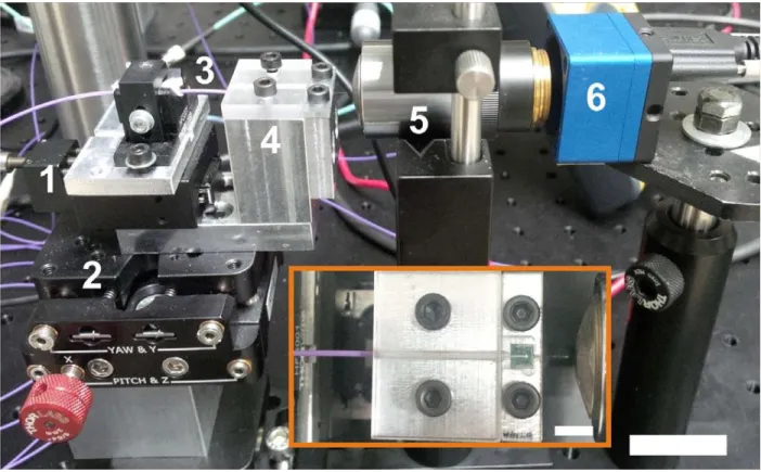
Figure 20: Photo of the waveguide efficiency measurement setup for chip scale optical characterization. The chip under test is inserted in a custom designed PMMA sample holder (4) fastened on a 3D translation stage (2). IR light (λ = 1310 nm) is delivered via a multimode fibre (3). The position of the fibre can be adjusted by a linear translation stage (1). Imaging (5) is made by a microscope objective (50×, NA = 0.8). All measured data are registered by a CMOS beam profiler (6). Scale bar shows 2 cm. The inset shows the top view of the fixed optrode chip
in the PMMA sample holder. Scale bar of the inset picture shows 5 mm. [24]
The waveguide efficiency of assembled, fully functional IR optrode devices was also observed. Figure 21. shows a photo of the setup of this measurement (cf. Fig. 19.A.):
37
Figure 21: Photo of the measurement setup to characterize waveguiding efficiency of fully packaged optrodes. Collimated IR light (λ = 1310 nm) emitted from a laser diode (1) is focused on the front facet of the multimode fibre (2), which is part of the optrode device. The PCB (3) of the optrode under test is fastened on a 3D translation stage. Imaging (4) the plane of the optrode
end facet is made by a microscope objective (50×, NA = 0.8). All measured data are registered by a CMOS beam profiler (5). Scale bar shows 2 cm. [96]
Similarly, the light emitted from a properly polished optical fibre was measured by the beam profiler first and set as reference intensity (Ifibre) after the background noise acquisition and compensation. Then this fibre was connected to an assembled IR optrode in the light path, and a similar measurement was taken (Ielectrode). The ratio of these measurements (Ielectrode / Ifibre) was considered as the overall waveguide efficiency of the optrode device (ηelectrode):
𝜂𝑒𝑙𝑒𝑐𝑡𝑟𝑜𝑑𝑒 = (𝐼𝑒𝑙𝑒𝑐𝑡𝑟𝑜𝑑𝑒
𝐼𝑓𝑖𝑏𝑟𝑒 ) (5)
The measurement setups introduced here (cf. Fig. 20 & 21.) provided images of the IR light beam profile emitted from the blunt tip of the Si chip (Fig. 23.A.). Through these images the incident beam spot size can be investigated acco rding to ISO 11146 standard.
3.6.2 Far field diffraction
If the microscope objective is removed from the light path (see Fig. 22.), we get far field diffraction image (Fig. 23.B.) of the IR light emitted from the blunt tip of the Si chip. We
1
2 4 3
5
38
can call it as far field, because the distance between the plane of observation and the aperture of light scattering surface is large enough (much larger than the wavelength and the characteristic size of the aperture). The surface of the end facet of Si waveguide (shaft of the optrode) is considered as a scattering surface covered with apertures of diffraction.
Although the initial scalloping caused by the DRIE etching was remarkably reduced (by step 13. on Fig. 15.), the sidewalls are not perfectly smooth (cf. [94]). Far field images were taken to evaluate beam divergence, because beam divergence depends primarily on diffraction present at the site of emission. These data were considered as practical initial conditions for a multiphysical modelling what was implemented to investigate the absorbed IR light’s thermal effect in the tissue. Csanád Örs Boros and colleagues first built the optical ray-tracing model of the IR optrode’s waveguiding modality concerning its surrounding ambience as air. My experiments validated the precision of this model [24].
Based on these experiences, they continued the development of the optical model concerning the possible effects of the brain tissue in case of implantation. Besides this optical model, they also built the finite element thermal model of the IR optrode in case of implantation. Later, they combined these two models into a coupled multi-physical (optical and thermal) model [112]. The outcomes of this combined model aided the design and the preparation of the in vivo experiments, which eventually validated both the thermal and the optical models concerning the brain tissue ambience [95].
39
Figure 22: Photo of the measurement setup to characterize beam divergence of fully packaged optrodes. Collimated IR light (λ = 1310 nm) emitted from a laser diode is focused on the front facet of the multimode fibre, which is part of the optrode device. The PCB of the optrode under test is fastened on a 5-axis stage. All measured data of far field images are registered by a CMOS beam profiler fastened on a remotely controlled motorized linear translation stage. Scale
bar shows 2 cm.
The same CMOS beam profiler was used to record far field diffraction pattern. It was fastened on a remotely operated precision linear translation stage (MTS50/M-Z8, Thorlabs Inc., USA), that provided acquisition at equidistant positions. The initial distance between the optrode’s blunt tip and the beam profiler’s sensor was set to 1 mm. After the background noise acquisition and compensation, sequential acquisitions with a 0.5 mm step-distance resolution were started (cf. Fig. 24.). Later, in chapter 4.3.2, the following
40
notations are used to quantify the angle of beam divergence (see Fig. 23.B.). Number of far field images used for evaluation are in brackets.
• Vertical: V1 pairs (n = 8) V2 pairs (n = 8)
• Horizontal: H1 pairs (n = 17) H2 pairs (n = 2)
The V1,V2 and H1,H2 labels do not represent exact maxima – which can be determined by the diffraction formula – only mark observable spots on each far field image acquired at equidistant positions, belonging to the same angle of beam divergence.
Figure 23: (A) IR light intensity distribution emitted from the blunt tip of the Si chip and (B) far field IR light intensity detector images recorded in the case of a representative optrode. The pixel intensity acquired with a CMOS beam profiler is in the same arbitrary units. Scale bars show 100 µm. Colours of the arrows on (B) represent pairs of diffraction maxima belonging to
the same angle of divergence. [24]
3.6.2.1 Calculation of beam divergence
Beam divergence characteristics is derived from analysis of the positions of diffraction maxima (see Fig. 23.B.). Using the notation of Fig. 24. the equation of a line is:
𝑦 = 𝑎 ⋅ 𝑧 + 𝑏, (6)

![Figure 8: Illustration of the optogenetic technique using a blue light, which activates ChR2- ChR2-expressing neuron cells by opening light sensitive ion channels [18]](https://thumb-eu.123doks.com/thumbv2/9dokorg/515134.207/14.918.190.726.101.495/figure-illustration-optogenetic-technique-activates-expressing-sensitive-channels.webp)
![Figure 13: Schematic of the design of functional chip with magnified view of the tip. All marked geometric dimensions are in [µm]](https://thumb-eu.123doks.com/thumbv2/9dokorg/515134.207/22.918.188.720.100.503/figure-schematic-design-functional-magnified-marked-geometric-dimensions.webp)

![Figure 19: Schematics highlighting the main components of an optical setup used to determine (A) beam profile and (B) optical power [96]](https://thumb-eu.123doks.com/thumbv2/9dokorg/515134.207/34.918.138.766.477.895/figure-schematics-highlighting-components-optical-determine-profile-optical.webp)