Vegard’s-law-like dependence of the activation energy of blistering on the x composition in hydrogenated a-SixGe1-x
Miklós Serényi1, Cesare Frigeri2 and Róbert Schiller1
1 Centre for Energy Research, Hungarian Academy of Sciences, P.O. Box 49, H-1525 Budapest (Hungary)
2 IMEM-CNR Institute, Parco Area delle Scienze 37/A, 43124 Parma (Italy)
* Corresponding author: serenyi.miklos@energia.mta.hu
ABSTRACT
Surface quality is a key issue in semiconductor structures for device applications. Typical surface defects are blisters. Here we investigate on the relationship between the activation energy of blistering and the composition x in hydrogenated amorphous a-SixGe1-x by employing layers deposited by Radio Frequency sputtering. To this aim the blistering activation energy was determined by means of Arrhenius plots in several samples with different compositions, including x=0 and x=1. Each sample was submitted to heat treatment up to the temperature where the onset of blistering was observed by change of the surface reflectivity. It is found that a linear dependence of the activation energy on x similar to the Vegard’s law holds. The experimental result is supported by reaction kinetics modeling. It is suggested that the key step for the formation of blisters is the scission of the SiH and GeH bonds. The related energetic reaction leading to the formation of H2 molecules in a-SixGe1-x
follows a linear law as a function of the x composition similarly to the activation energy.
Keywords : Amorphous SiGe; Blisters; Hydrogen; Annealing; Sputtering; Solar cells
1. Introduction
The degradation of the surface quality of several types of material is often due to the formation of blisters [1-6]. Blistering is caused by voids inside the material which have reached a sufficient size to touch and deform the surface because of the increased pressure of some gas inside the voids [1-8]. In the worst cases blisters burst leaving craters [1, 6, 8-11].
The gas is almost always H or He. It is introduced into the material in different ways, e.g. by implantation [1, 2, 10-15], mixed or in compounds with other gases employed to grow a given material in a plasma regime in the case of H [6, 16, 17]. Hydrogen and He are hardly soluble in most materials with the consequence that they tend to segregate into voids that grow and coalesce upon annealing with an ensuing increase of the gas pressure [14]. The surface blistering of ion-implanted materials is still object of detailed research [1, 10, 12-14, 18]. As for semiconductors plenty of work has been carried out for H and/or He implanted materials especially with the aim to optimize the smart-cut technique based on wafer bonding [4, 11, 14, 15, 18-21]. Much less work has been done for not implanted semiconductors. Among them are hydrogenated a-Si (amorphous Si), a-Ge and their alloy a-SixGe1-x that find applications insolar cells [16, 17, 22-28]. As regards a-Ge and a-SixGe1-x they are also very suitable for IR radiation sensors [29], like un-cooled microbolometers [30], thin films transistors [31], detectors for X- or γ-ray imaging [16] and fiber-optic systems[32]. For such applications hydrogenation is always applied since H reduces, by even an astounding 4 orders of magnitude [33], the density of the dangling bonds which are harmful for the electro-optical performance of the devices since they act as carrier trapping and recombination centres.
Hydrogen is most often introduced during growth, as it was said earlier. Obviously, besides optimal electro-optical properties the structural (surface) integrity must also be preserved, e.g.
by preventing formation of blisters.
The procedure to grow a-Si, a-Ge and a-SixGe1-x ,e.g. by chemical vapour deposition (CVD) in its various configurations [16, 17, 24, 25, 34] as well as the manufacturing processes to get the final device [35] very often require some heating of those materials. Such annealing can give rise to blisters due to the enhancement of the pressure inside the voids containing H as recalled earlier in this Introduction and experimentally demonstrated in Si and Ge [8, 20, 21, 36] and c-SiGe [10, 11]. Degradation of the layer surface upon annealing has also been reported in not hydrogenated materials like, e.g., perovskite based structures for photovoltaic devices [37, 38]. The activation energy of blistering has been the object of several studies [10, 11, 14, 15, 19-21, 36]. In fact, its knowledge through the use of simple
Arrhenius plots is very useful to enlighten the origin of the rate-limiting step in the blistering process hence its physical-chemical mechanisms [10, 11, 14, 15, 19-21, 36].
The aim of this paper is to investigate such mechanisms in not-implanted hydrogenated a- SixGe1-x alloys by measurement of the blistering activation energy and to establish a law to evaluate it as a function of x. It will be shown that this law is similar to the Vegard’s one. The samples of this work have been grown by radio frequency (RF) sputtering which does not need to heat up the sample during sputtering of the target material. This guarantees that, before the after-growth annealing experiments applied for the determination of the activation energy, the samples did not undergo any annealing with possible blister formation during sample growth which can be harmful for the correct evaluation of the blistering onset.
Additionally, RF sputtering has the advantage that H containing toxic gases like silane and germane employed in the CVD reactors are not used. Moreover, the incorporation of H is simply controlled by gas flow meters and does not need the dissociation of those gases which may depend on the substrate temperature. It is also a versatile technology and appropriate to prepare series of samples with different compositions. Its highly reproducible performance was demonstrated in an earlier work of us [39].Differently from implanted samples where the activation energy is determined by the blistering associated with the splitting of an implanted layer from a substrate, [10, 11] here the activation energy is a ‘’pure’’ one, i.e., experimentally measured only by the sudden appearance of surface blisters. Exfoliation of the deposited layers from the substrate has not been observed.
2. Experiment
The investigated samples were hydrogenated a-SixGe1-x (0≤x≤1) obtained by RF sputtering from targets of either pure Si, pure Ge or a target assembled from different size of Si and Ge slices. As substrates polished(100) c-Si wafers were used. They were mounted on a water cooled stage 50 mm away from the target to reduce heating up of the substrate caused by the impinging Si and/or Ge atoms released by the target. This assured that the substrate temperature was always ≤ 60 °C [39]. The target was coupled to an RF generator operating at 13.56 MHz. The chamber was evacuated by a turbo molecular pump to a basic pressure of 510-5 Pa. The RF sputtering has been carried out under a mixture of hydrogen and argon high purity gases with an applied wall potential of 1.5 kV dc yielding a plasma pressure of 2.5x10⁻² mbar. The hydrogen flow rate was kept constant at a value of 0.9% of the 2.5x10⁻² mbar plasma pressure for all the deposited a-SixGe1-x layers. The H content was 16-18 at% as
measured by ERDA (Elastic Recoil Detection Analysis) while the x composition was determined by ERDA and EDS (Energy Dispersive Spectroscopy) in a TEM (Transmission Electron Microscope). The sputtered layers were mirror-like and had a thickness around 200 nm. Besides pure Si and Ge, SixGe1-x layers of five different compositions of x=0.32, 0.44, 0.67, 0.74 and 0.96 have been prepared (Table 1).
Table 1
Composition x of the SixGe1-xsamples vs sample number
The activation energy Ea for blistering was determined by Arrhenius plots reporting the inverse of the minimum time needed to make the blisters optically visible as a function of the inverse of the temperature. The temperature range investigated was different depending on the analysed sample. It varied from a minimum of 179 °C (for pure a-Ge) to a maximum of 271
°C (for pure a-Si). Such temperatures are much lower than the crystallization temperature of Ge and Si. As recalled in Ref. [8] and references therein, it varies between 450 and 490 °C for Ge and between 700 and 740 °C for Si. For a-SixGe1-x crystallization is reported to occur at temperatures ≥ 550 °C unless a catalityc metal is used [40, 41] which was not our case. The amorphous state of our annealed samples was confirmed experimentally by TEM (Fig. 1).The hydrogenated samples have been heated in air on a plate at constant temperature ( 1 °C) while illuminated by a 3 mW He-Ne laser beam with diameter of 3 mm and angle of incidence of 60° which resulted in an elliptically illuminated sample area with size of about 3x6 mm2 (Fig. 2). The onset time of blistering was the time elapsed between the stabilization of the temperature and the start of the decrease of the reflectivity of the sample surface.
After reflection the radiation fell onto an Si PIN detector blended with diameter of 3 mm.
During the heating process the specular reflection transforms into a spread one, which has a dominant directional component that is partially diffused by surface irregularities (Fig. 2).
The onset of blistering was identified with the sudden decrease of the reflected intensity caused by the outgoing rays reflected at many different angles. The sampling rate of the reflection monitoring was 5-10 sec.
Sample # 1 2 3 4 5 6 7
Composition
x 0 0.32 0.44 0.67 0.74 0.96 1
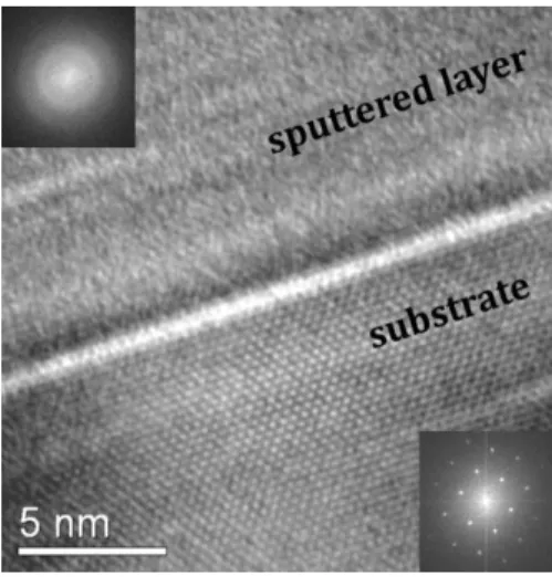
Fig. 1. HR-TEM (high resolution TEM) image taken from the a-Si sample (x=1) after annealing. In this sample the temperature for the blistering onset was the highest.
The inset FFT (Fast Fourier Transform) spectra clearly show the amorphous state of the sputtered layer opposite to the crystalline state of the substrate.
Fig. 2. Sketch of the experimental procedure for detecting the onset of blistering.
3. Results
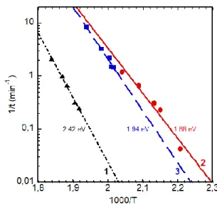
Fig. 3 shows a typical Arrhenius plot of an a-SixGe1-x sample along with those of a-Si and a-Ge. The example given for a-SixGe1-x is for x=0.44. The blistering activation energy for a-Si and a-Ge is 2.42 and 1.68 eV, respectively, while the activation energies of the a-SixGe1-x
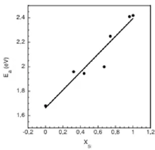
samples were in-between those two values. The activation energy of the a-SixGe1-x was seen to decrease linearly with decreasing x. This is displayed in Fig. 4 giving the blistering activation energy Ea in the a-SixGe1-x alloys, Ea(SixGe1-x), as a function of the x composition.
The fitting curve is
Ea = Ea(SixGe1-x) = 1.663 + 0.733•x (1)
Fig. 3. Arrhenius plots 1/t (min-1) = kexp vs 1000/T (K-1) for a-Si (dot-dashed black curve 1), a-Ge (full red curve 2) along with a typical one for a-Si0.44Ge0.56 (dashed blue curve 3).
The blistering activation energy is indicated aside each curve.
Fig. 4. Blistering activation energy Ea(SixGe1-x) in SixGe1-x as a function of x. The equation of the fitting curve is Ea(SixGe1-x) = 1.663 + 0.733·x.
Let E2a (=2.42 eV) and E3a (=1.68 eV) indicate the experimental activation energies for blistering in a-Si and a-Ge, respectively. By recognizing that in eq. (1) the factor multiplying the composition x is equal, within 1%, to (E2a - E3a) = 0.74 eV and that 1.663 is equal, within 1%, to E3a the experimental relationship between Ea(SixGe1-x), E2a and E3a can be expressed as
Ea (SixGe1-x) = E3a + x•( E2a - E3a) = x•E2a + (1-x) •E3a (2) It is concluded that the activation energy of blistering in a-SixGe1-x is related to the activation energies in a-Si and a-Ge through a linear relationship as a function of the x composition in an equation remembering the Vegard’s law [42] typically valid for the lattice parameter [42] and energy band gap [43] in compound semiconductors.
4. Discussion
As shown elsewhere [36, 39] and assumed in several works [11, 14, 19] the blisters are due to the increase of size of voids/bubbles containing molecular hydrogen H2 in the samples.
Our earlier works revealed that blisters with typical dimensions of about 1-2 µm appear uniformly on the surface in the case of Si [39] and Ge [36] layers. Based on this, we can
assume that blistering occurs at the time tbl when the number of the accumulated H2 molecules reach the critical Nbl number and the critical pressure as a consequence of the general gas law.
This cannot occur in the case of the different SiGe alloys otherwise, therefore the accumulation process in time can be described by
kexp·t = NH/Nbl (3)
where kexp is the rate coefficient of reaction and NH the number of accumulated H2 molecules.
Inserting the time of appearance of blisters observed in the experiments we get a simple relation enabling the Arrhenius plot to explore atomic scale processes
kexp·tbl = 1 or ln kexp = – ln tbl (4)
In the a-SixGe1-x system the atomic H for the formation of H2 is supplied by the rupture of its bonds to Si and Ge according to the following reactions
SiH Si+H (5) GeH Ge+H (6) H+H H2 (7) Let [MeH] = [SiH] + [GeH] represent the total metal hydride concentration in the layer, with the parenthesis [] indicating concentrations, and k2, k3 and k4 the rate coefficients of reactions (5) to (7), respectively. The reaction kinetics governing the evolution in time of the concentration of H2, d[H2]/dt, can be derived by using the following kinetic differential equations for 0<x<1
d H
dt k
2x MeH k
3(1x) MeH 2k
4 H
2
(8)
d H
2dt 2k4
H 2 (9)According to the Bodenstein approximation [44], d[H]/dt= 0, therefore
d H
2dt k2x MeH
k3(1x) MeH
ke x p
MeH
(10) i.e.
k2x + k3(1-x) = kexp (11)
where kexp is the rate coefficient for the SiGe alloy.
From kexp = k0exp(-Ea/kBT), with k0 the pre-exponential factor, kB the Boltzmann’s constant (8.62∙10-5 eV·K−1), T the temperature in K and Ea the activation energy for blistering in the SiGe alloy, the latter one can be expressed as
Ea x k2
kex pE2 a(1x) k3 kex pE3 a (12)
provided that the activation energy Ea does not depend on T in the range of the applied annealing temperature. By entering eq. (11) in eq. (12) after some mathematical treatment one gets
Ea x k2
kex pE2 a(1x) k3
kex pE3 a (13)
where E2a and E3a are the blistering activation energies in a-Si and a-Ge, respectively. By substituting kexp by k2x + k3(1-x) from eq. (11) and with | k2 - k3 | << k3, i.e. k2 ≈ k3, (see Appendix) one finally obtains
Ea = x•E2a + (1-x)•E3a (14)
which is a Vegard’s-law-like equation relating the activation energy of blistering in a-SixGe1-x to the activation energies in a-Si (E2a) and a-Ge (E3a). Eq. (14) is just the same as eq. (2).
To the best of the Authors’ knowledge for Si, Ge and SiGe the activation energy for blister formation has only been determined in implanted crystalline samples for which some scatter exists since it was seen that it varies depending on the implant dose, annealing temperature and also doped/not-doped status. Most often the activation energies turned out to be somewhat close, but smaller, to ours only when the annealing temperature was low (≤ 500
°C), being otherwise significantly smaller, on the order of 1 eV and even less [10, 11, 15, 19, 20]. Table 2 summarizes the most significant literature data about the blistering activation energy in Si, Ge, SiGe. In some cases, in order to explain the measured activation energies for blistering, e.g. 1.2 and 1.0 eV for Si and Ge, respectively, even at low temperatures [15], it was suggested [11, 15] that the first step for the generation of the blisters could be the rupture of SiSi and GeGe bonds, respectively, despite the fact that the experimental values of the activation energies were much smaller, by 50-60 % [15] and 75% [11], with respect to the literature values for the bond energies of SiSi and GeGe used as references in those papers. It
should also be noticed that the break of the SiSi and GeGe bonds does not supply any free H.
So, in the frame of this hypothesis it would be quite unlikely that blisters form. Furthermore, that hypothesis would imply a reduction of the density of free H since the break of SiSi and GeGe bonds would make available free dangling bonds where H can attach to. It is proposed here that the initial step for the formation of blisters is rather the break of the SiH and GeH bonds whereby free H is produced according to eqs. (5) and (6).
Table 2
Literature data of the blistering activation energies in hydrogenated Si, Ge and SiGe
Material Reference Activation
Energy (eV)
Notes
c-Si, implanted
7 1.2
13 2.5 For T <500 °C
11 1-2.6 Dose dependent
c-Ge, implanted 7 1
11 1.75
c-Si0.70Ge0.30
implanted
4 1.32 For T < 400 °C.
Doping dependent
5 1.60 For T < 350-425 °C
a-Si This work 2.42
a-Ge This work 1.68
a-SixGe1-x This work
Varies with x between those of
a-Si and a-Ge
Vegard’s law Eq. (1) and Eq. (14)
The energetic balance associated with reactions (5) to (7) would support our hypothesis.
For both the SiH and GeH bonds in literature there are different values for their binding energy in amorphous Si and Ge. In this paper the average among them is used. For SiH that average is made among the data reported in the seven references [45-51] and it is (SiH) = 3.45 eV. As to GeH, the data of five papers are used [47, 52-56] yielding an average value of
(GeH) = 3.10 eV. A general consensus exists that the bond energy of H2 is (H2) =4.50 eV [45, 46].
Let us first consider a-Si (x=1). The break of only one SiH bond does not account for the observed E2a. However, the break of two SiH bonds with simultaneous formation of a hydrogen molecule, implies a change of energy = 2•(SiH) -(H2) = 2.40 eV which is very close to our experimental blistering activation energy in a-Si (E2a = 2.42 eV). Also for a- Ge a close agreement between the measured activation energy of E3a = 1.68 eV and our model exists since for a-Ge the model gives the following energetic balance: = 2•(GeH) -(H2)
= 1.70 eV. The slight disagreement between measured and estimated activation energies can be ascribed to experimental errors on the collected experimental data and to the scatter of the literature data regarding the bonding energy of SiH and GeH,(SiH) and (GeH). The proposed energetic model also works for the a-SixGe1-x alloy if a Vegard’s-law-like dependence is applied for the evaluation of , i.e.
SixGe1-x = 2•[ x•(SiH) + (1-x) •(GeH)] -(H2) = Ea (SixGe1-x) (15)
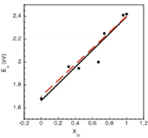
Eq. (15) also stems from eq. (2) or (14) by replacing E2a by 2•(SiH) -(H2) and E3a by 2•(GeH) -(H2). Such dependence is validated by comparison with the experiment. Fig. 5 shows again the experimental activation energies (black dots) as a function of the x composition of a-SixGe1-x along with thefitting curve (black solid line). The dashed red curve represents eq. (15). The agreement is very good. In a-SixGe1-x the measured activation energy for blistering onset, Ea = Ea (SixGe1-x), is thus an effective activation energy resulting from the energy balance between the rupture of the two H-host atom bonds and the creation of the H2
molecule. This analysis shows that the overall process 2MeHH2 is endotherm for any x value, and practically no energy of activation is needed above the thermodynamic barrier.
Fig. 5. Same as Fig. 4 with the addition of the dashed red curve representing eq. (15), i.e.
SixGe1-x = 2·[ x·(SiH) + (1-x)·(GeH)] -(H2), with (SiH) = 3.45 eV and
(GeH) = 3.10 eV.
A perfect coincidence between experiment and eq. (15) could be obtained by using
(GeH) = 3.08 eV instead of 3.10 eV. Apart from the experimental errors, this shows that the agreement depends on the reference values chosen for (GeH) and (SiH). It is believed that the choice made here of using the average among the various literature values of (GeH) and
(SiH) may guarantee the better evaluation of the reaction kinetics and mechanisms governing the formation of blisters in a-SixGe1-x, 0≤ x ≤1.
Estimates from our data would also allow to establish the dependence on the x composition of the temperature Tbl of blistering (which occurs after e.g. one minute). It can be expressed as
1000/Tbl =1.86x+2.05(1-x)
which is still of the Vegard’s type as concerns the inverse of Tbl. However, this should not be an appropriate feature of the blistering process and should be dealt with care. In fact, the onset of blistering strongly depends on the thickness of the layer and is very sensitive to the H content. Therefore, only samples from the same growth process, i.e. with the same thickness and H content, can be compared each other as regards the relationship between 1/Tbl and x.
The latter relationship and the related influence of sample thickness and H content will be the
object of more detailed investigations in the future. Its knowledge can be very useful as it can help to estimate the lifetime of thin film solar cells or any other device.
5. Conclusions
The activation energy for the formation of surface blisters in hydrogenated a-SixGe1-x has been found to be related to the blistering activation energies of pure a-Si and a-Ge through the composition x in a simple linear relationship similar to the Vegard’s law valid for the lattice parameter or energy band gap of a binary compound. Blisters form when voids containing H2
gas can increase their volume as a consequence of heat treatments. The model presented here ascribes the formation of H2 to the reaction between two H atoms produced by the break of SiH and GeH bonds upon annealing. By taking for the bond energies of SiH, GeH and H2 the average valuesamong several literature data full compatibility of our model with experimental results is achieved thus confirming the validity of the model. It should be noticed that the temperature range at which blistering onset was detected, i.e. from 179 °C (for pure a-Ge) to 271 °C (for pure a-Si), concerns temperatures often applied for the a-SixGe1-x growth, e.g. by CVD, or during device manufacturing processes and close to the operating temperature of solar cells.
Acknowledgements
Work supported by the Scientific Cooperation Agreement between CNR (Italy) and MTA (Hungary). Grateful thanks for the cooperation are due to A. Csík, A. Hámori and Z. Zolnay.
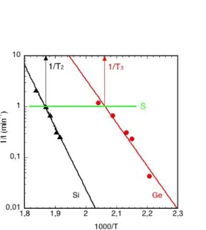
APPENDIX
Let us define a line as a new abscissa of a coordinate transformation (green in Fig. A1) ln kexp = –ln ts = ln S.
S is a „shift in time”; for example if S=1, then 1/ts =1 min-1 taken into account the measured inverse time–inverse temperature pairs of Fig. 3. The fitted line of the measured data of Si and Ge intersects the abscissa S at 1/T2 and 1/T3:
ln k2(T2) = ln k3(T3)= ln S (A1)
Fig. A1. Arrhenius plots 1/t (min-1) = kexp vs 1000/T (K-1) for a-Si (dot-dashed black curve Si), a-Ge (full red curve Ge) and the new abscissa (green line).
Entering the form of reaction rate kexp = k0·exp(-Ea/kBT) into the Eq. (A1) results in
k2 0eE2 a/ kBT2 = k3 0eE3 a/ kBT3 = S simplified to:
k2SevE2a where
v 1 kB
1 T1
T2
and
k
3S e
wE3a where w 1kB 1 T1
T3
(A2)
Applying eq. (12), we can determine the partial derivatives:
k2/vk2E2a and
k3/wk3E3a
Using the linearized form of eq. (11) in the range of T2>T>T3 for v and w values small enough we get
By using the first order of the series expansion of the logarithmic function, i.e. ln(1-y) ≈ -y , we can write
lnkexp - lnS ≈ xE2av + (1-x)E3a w
By entering the definition of eq. (A2) the above equation becomes:
lnke xplnS
x E2a1xE3a
1kBT x E2a
T2 1xE3a
T3
1 kB This is a function having a form of
xE2a
1x
E3a
1kBTconst
which is a Vegard’s-law-like function relating the activation energy of blistering and 1/T. The
“const” is the ordinate intercept. It does not have too much importance and, anyway, the position of the line “de facto” depends on the thickness of the deposited layer (the evolution of blister slows down in the thicker layers). The “S ” can be swept up or down drawing a horizontal line. The line can be positioned everywhere in the measured region and the multiplier of 1/kBT does not depend of the position of the chosen S, for any S≠ 0. It should be noted that the difference T2 - T3 becomes smaller with increasing temperature (i.e. v≈w) and the condition | k2 – k3 | << k3, i.e. k2 ≈ k3,ispractically fulfilled at the temperature of about 710 K where the blistering time would be only on the order of microseconds.
References
[1] Da Chen, Dadi Wang, Yongwei Chang, Ya Li, Rui Ding, Jiurong Li, Xiao Chen, Gang Wang, and Qinglei Guo, Exceptional cracking behavior in H-implanted Si/Bdoped Si0.70Ge0.30/Si heterostructures, Appl. Phys. Express 11 (2018) 011301.
[2] Congwei Ji, Shaojie Zhang and Hehui Wang, Simulation Analysis of the Mutual Influence of the Stress Intensity Factor on the Multiple Blisters Caused by Hydrogen Induced Damage, IOP Conf.
Ser.: Mater. Sci. Eng. 322 (2018) 042014
[3] Jun Wang, Long Cheng, Yue Yuan, Shao-Yang Qin, Kameel Arshad, Wang-Guo Guo, Zheng Wang, Zhang-Jian Zhou, Guang-Hong Lu, Blistering behavior and deuterium retention in tungsten vanadium alloys exposed to deuterium plasma in the linear plasma device STEP, J. Nucl. Mater.
500 (2018) 366-372
[4] Da Chen, Nan Zhang, Bei Wang, Anli Xu, Ya Li, Siwei Yang, Gang Wang, and Qinglei Guo, Controllable cracking behavior in Si/Si0.70Ge0.30/Si heterostructure by tuning the H+ implantation energy, Appl. Phys. Lett. 111 (2017) 062104
[5] Mikael Broas, Hua Jiang, Andreas Graff, Timo Sajavaara, Vesa Vuorinen, and Mervi Paulasto- Kröckel, Blistering mechanisms of atomic-layer-deposited AlN and Al2O3 films, Appl. Phys. Lett.
111 (2017) 141606
[6] C. Frigeri, M. Serényi, Zs. Szekrényes, K. Kamarás, A. Csik, N. Q. Khánh, Effect of heat treatments on the properties of hydrogenated amorphous silicon for PV and PVT applications, Sol. Energy 119 (2015) 225-232
[7] Pascal Genevée, Ernest Ahiavi, Norik Janunts, Thomas Pertsch, Maria Oliva, Ernst-Bernhard Kley, and Adriana Szeghalmi, Blistering during the atomic layer deposition of iridium, J. Vac. Sci.
Technol. A 34 (2016) 01A113.
[8] C. Frigeri, M. Serényi, N. Q. Khánh, A. Csik, L. Nasi, Z. Erdélyi, D. L. Beke and H.-G. Boyen, Hydrogen behaviour in amorphous Si/Ge nano-structures after annealing, Appl. Surf. Sci. 267 (2013) 30-34
[9] C. Frigeri, L. Nasi, M. Serényi, A. Csik, Z. Erdélyi, and D. L. Beke, TEM and AFM study of hydrogenated sputtered Si/Ge multilayers, Superlattice. Microst. 45 (2009) 451-457
[10] Da Chen, Qinglei Guo, Nan Zhang, Bei Wang, Anli Xu, Ya Li, Siwei Yang, and Gang Wang, Investigation of low-fluence hydrogen implantation-induced cracking in B doped Si0.70Ge0.30, J.
Vac. Sci. Technol. B 35 (2017) 041203
[11] R. Singh, R. Scholz, S. Christiansen, S. Mantl, and M. Reiche, Investigation of a hydrogen implantation-induced blistering phenomenon in Si0.70Ge0.30, Semicond. Sci. Technol. 26 (2011) 125001
[12] N. Daghbouj, N. Cherkashin, F.-X. Darras, V. Paillard, M. Fnaiech, and A. Claverie, Effect of the order of He+ and H+ ion co-implantation on damage generation and thermal evolution of
complexes, platelets, and blisters in silicon, J. Appl. Phys. 119 (2016) 135308
[13] U. Dadwal, D. Buca, S. Mantl, T. Wernicke and R. Singh, Investigation of blistering process in H-implanted semipolar GaN, Scr. Mater. 94 (2015) 21–24
[14] B. Terreault, Hydrogen blistering of silicon: Progress in fundamental understanding, phys. stat.
sol. (a) 201 (2007) 2129-2184
[15] Q.-Y. Tong, K. Gutjahr, S. Hopfe, U. Gösele, T.-H. Lee, Layer splitting process in hydrogen- implanted Si, Ge, SiC, and diamond substrates, Appl. Phys. Lett. 70 (1997) 1390-1392
[16] V. Steenhoff, A. Neumüller, O. Sergeev, M. Vehse and C. Agert, Integration of a-Ge:H nanocavity solar cells in tandem devices, Sol. Energy Mater. Sol. Cells 145 (2016) 148-153 [17] L. W. Veldhuizen, C. H. M. van der Werf , Y. Kuang, N. J. Bakker, S. J. Yun, R. E. I. Schropp,
Optimization of hydrogenated amorphous silicon germanium thin films and solar cells deposited by hot wire chemical vapor deposition, Thin Solid Films 595 (2015) 226-230
[18] Zhongying Xue, Da Chen, Pengfei Jia, Xing Wei, Zengfeng Di, Miao Zhang, The reduction of critical H implantation dose for ion cut by incorporating B-doped SiGe/Si superlattice into Si substrate, Appl. Surf. Sci. 385 (2016) 42–46
[19] S. W. Bedell and W. A. Lanford, Investigation of surface blistering of hydrogen implanted crystals, J. Appl. Phys. 90 (2001) 1138-1146
[20] Fan Yang, Xuan Xiong Zhang, Tian Chun Ye, and Song Lin Zhuang, The investigation on surface blistering of Ge implanted by hydrogen under the low temperature annealing, J.
Electrochem. Soc. 158 (2011) H1233-H1237
[21] M. Bruel, The history, physics, and applications of the Smart-Cut process, Mater. Res. Soc. Bull.
23 (1998) 35-39
[22] Bart Macco, Jimmy Melskens, Nikolas J. Podraza, Karsten Arts, Christopher Pugh, Owain Thomas, and Wilhelmus M. M. Kessels, Correlating the silicon surface passivation to the nanostructure of low-temperature a-Si:H after rapid thermal annealing, J. Appl. Phys. 122 (2017) 035302
[23] Xin Zhao, Dun Li, Tian Zhang, Brianna Conrad, Li Wang, Anastasia H. Soeriyadi, Jianshu Han, Martin Diaz, Anthony Lochtefeld, Andrew Gerger, Ivan Perez-Wurfl, Allen Barnett, Short circuit current and efficiency improvement of SiGe solar cell in a GaAsP-SiGe dual junction solar cell on a Si substrate, Sol. Energy Mater. Sol. Cells 159 (2017) 86–93
[24] Fai Tong Si, Olindo Isabella, Miro Zeman, Thin-film amorphous silicon germanium solar cells with p- and n-type hydrogenated silicon oxide layers, Sol. Energy Mater. Sol. Cells 163 (2017) 9-14
[25] G. H. Wang, C.Y. Shi, L. Zhao, H. W. Diao, W. J. Wang, Fabrication of amorphous silicon- germanium thin film solar cell toward broadening long wavelength response, J. Alloys Compd.
658 (2016) 543-547
[26] J-W. Schüttauf, B. Niesen, L. Löfgren, M. Bonnet-Eymard, M. Stuckelberger, S. Hänni, M.
Boccard, G. Bugnon, M. Despeisse, F-J. Haug, F. Meillaud, C. Ballif, Amorphous silicon–
germanium for triple and quadruple junction thin-film silicon based solar cells, Sol. Energy Mater. Sol. Cells 133 (2015) 163–169
[27] Duy Phong Pham, Sangho Kim, Jinjoo Park, Anh Huy Tuan Le, Jaehyun Cho, Junsin Yi, Improvement in carrier collection at the i/n interface of graded narrow-gap hydrogenated amorphous silicon germanium solar cells, J. Alloys Compd. 724 (2017) 400-405
[28] Emna Kadri, Olfa Messaoudi, Monem Krichen, Khaled Dhahri, Mohammed Rasheed, Essebti Dhahri, Abdelaziz Zouari, Kamel Khirouni, Régis Barillé, J. Alloys Compd. 721 (2017) 779-783 [29] Sang Youn Han, Kyung Sook Jeon, Junho Song, Ho Sik Jeon, and Byung Seong Bae, Photo-
related stress effects in a-SiGe:H thin film transistors for infrared image sensors, J. Display Technol. 9 (2013) 30-36
[30] M. Moreno, N. Delgadillo, A. Torres, R. Ambrosio, P. Rosales, A. Kosarev, C. Reyes-Betanzo, J.
de la Hidalga-Wade, C. Zuniga, W. Calleja, Boron doping compensation of hydrogenated amorphous and polymorphous germanium thin films for infrared detection applications, Thin Solid Films 548 (2013) 533-538
[31] M. Dominguez, P. Rosales, A. Torres, F. Flores, J. Molina, M. Moreno, J. Luna, A. Orduña, Planarized ambipolar a-SiGe:H thin-film transistors: Influence of the sequence of fabrication process, Solid State Electron. 99 (2014) 45-50
[32] M. A. Ettabib, C. Lacava, Z. Liu, A. Bogris, A. Kapsalis, M. Brun, P. Labeye, S. Nicoletti, D.
Syvridis, D. J. Richardson and P. Petropoulos, Wavelength conversion of complex modulation formats in a compact SiGe waveguide, Opt. Express 25 (2017) 3252-3258
[33] S. Jin and L. Ley, Hydrogen-related defects in hydrogenated amorphous semiconductors, Phys.
Rev. B 44 (1991) 1066-1073
[34] Jia Fang, Ze Chen, Ning Wang, Lisha Bai, Guofu Hou, Xinliang Chen, Changchun Wei, Guangcai Wang, Jian Sun,Ying Zhao, Xiaodan Zhang, Improvement in performance of hydrogenated amorphous silicon solar cells with hydrogenated intrinsic amorphous silicon oxide p/i buffer layers, Sol. Energy Mater. Sol. Cells 128 (2014) 394–398
[35] G. H. Wang, C. Y. Shi, L. Zhao, R. D. Hu, L. L. Li, G. Wang, J. W. Chen, H. W. Diao, W. J.
Wang, Performance improvement of amorphous silicon germanium single junction solar cell modules by low temperature annealing, Thin Solid Films 552 (2014) 180-183
[36] M. Serényi, C. Frigeri, A. Csik, N. Q. Khánh, A. Németh, Z. Zolnai, On the mechanisms of hydrogen induced blistering in RF sputtered amorphous Ge, CrystEngComm 19 (2017) 1486- 1494
[37] Pariya Nazari, Fatemeh Ansari, Bahram Abdollahi Nejand, Vahid Ahmadi, Masoud Payandeh, and Masoud Salavati-Niasari, Physicochemical Interface Engineering of CuI/Cu as Advanced Potential Hole-Transporting Materials/Metal Contact Couples in Hysteresis-Free Ultralow-Cost and Large-Area Perovskite Solar Cells, J. Phys. Chem. C 121 (2017) 21935−21944
[38] Fatemeh Ansari, Pariya Nazari, Masoud Payandeh, Farzad Mardekatani Asl, Bahram Abdollahi- Nejand, Vahid Ahmadi, Jalal Taghiloo and Masoud Salavati-Niasari, Novel nanostructured electron transport compact layer for efficient and large-area perovskite solar cells using acidic treatment of titanium layer, Nanotechnology 29 (2018) 075404
[39] C. Frigeri, M. Serényi, N. Q. Khánh, A. Csik, F. Riesz, Z. Erdélyi, L. Nasi, D. L. Beke and H.-G.
Boyen, Relationship between structural changes, hydrogen content and annealing in stacks of ultrathin Si/Ge amorphous layers, Nanoscale Res. Lett. 6 (2011) 189
[40] Kaoru Toko, Hiroshi Kanno, Atsushi Kenjo, Taizoh Sadoh, Tanemasa Asano, Masanobu Miyao, Low-temperature solid-phase crystallization of amorphous SiGe films on glass by imprint technique, Solid-State Electron. 52 (2008) 1221-1224
[41] Chuan-Jung Lin, Chien-Chung Hsu, Sheng-Min Yu, Yu-Chun Huang, Sung-Yen Wei, Wen- Ching Sun, Tzer-Shen Lin and Fu-Rong Chen, Growth mechanism of an aluminium-induced solid phase epitaxial (AI-SPE) Si0.5Ge0.5 layer using in situ heating transmission electron microscopi, CrystEngComm 18 (2016) 3556-3560
[42] L. Vegard, Die Konstitution der Mischkristalle und die Raumfüllung der Atome, Zeits. Phys. 5 (1921) 17-26
[43] B. Streetman and S. Banarjee, Solid State Electronic Devices, Ch. 1, 6th edition (Prentice Hall, 2005)
[44] T. Turányi and A. S. Tomlinson, Analysis of Kinetic Reaction Mechanisms (Springer, Berlin, 2014)
[45] W. Beyer, Hydrogen effusion: a probe for surface desorption and diffusion, Physica B 170 (1991) 105-114
[46] P. Gupta, V. L. Colvin, and S. M. George, Hydrogen desorption kinetics from monohydride and dihydride species on silicon surfaces, Phys. Rev. B 37 (1988) 8234-8243
[47] R. Tsu, D. Martin, J. Gonzales-Hernandez, and S. R. Ovshinsky, Passivation of dangling bonds in amorphous Si and Ge by gas adsorption, Phys. Rev. B 35 (1987) 2385-2390
[48] K. Zellama, P. Germain, S. Squelard, B. Bourdon, J. Fontenille, and R. Danielou, Possible configurational model for hydrogen in amorphous Si:H. An exodiffusion study, Phys. Rev. B 23 (1981) 6648-6667
[49] D. C. Allan, J. D. Joannopoulos, and W. B. Pollard, Electronic states and total energies in hydrogenated amorphous silicon, Phys. Rev. B 25 (1982) 1065-1080
[50] Chris G. Van de Walle and R. A. Street, Silicon-hydrogen bonding and hydrogen diffusion in amorphous silicon, Phys. Rev. B 51 (1995) 10615-10618
[51] G. Lucovsky, Z. Jing, Z. Lu, D. R. Lee, J. L. Whitten, Properties of bonded hydrogen in hydrogenated amorphous silicon and other hydrogenated amorphous silicon alloys, J. Non-Cryst.
Solids 182 (1995) 90-102
[52] A. Arrais, P. Benzi, E. Bettizzo and C. Damaria, Correlations among hydrogen bonding
configuration, structural order and optical coefficients in hydrogenated amorphous germanium obtained by x-ray-activated chemical vapour deposition, J. Phys. D: Appl. Phys. 42 (2009) 105406
[53] G. A. N. Connell and J. R. Pawlik, Use of hydrogenation in structural and electronic studies of gap states in amorphous germanium, Phys. Rev. B 13 (1976) 787-804
[54] R. A. Street, Model for growth of a-Si and its alloys, Phys. Rev. B 44 (1991) 10610-10616 [55] G. Lucovsky, Hydrogen in amorphous silicon: local bonding and vibrational properties, J. Non-
Cryst. Solids 141 (1992) 241-256
[56] L. Battezzati, F. Demichelis, C. F. Pirri, and E. Tresso, Differential scanning calorimetry (DSC) studies of hydrogenated amorphous semiconductor alloys, Physica B 176 (1992) 73-77
Figure Captions
Fig. 1. HR-TEM (high resolution TEM) image taken from the a-Si sample (x=1) after annealing. In this sample the temperature for the blistering onset was the highest. The inset FFT (Fast Fourier Transform) spectra clearly show the amorphous state of the sputtered layer opposite to the crystalline state of the substrate.
Fig. 2. Sketch of the experimental procedure for detecting the onset of blistering.
Fig. 3. Arrhenius plots 1/t (min-1) = kexp vs 1000/T (K-1) for a-Si (dot-dashed black curve 1), a-Ge (full red curve 2) along with a typical one for a-Si0.44Ge0.56 (dashed blue curve 3).
The blistering activation energy is indicated aside each curve.
Fig. 4. Blistering activation energy Ea(SixGe1-x) in SixGe1-x as a function of x. The equation of the fitting curve is Ea(SixGe1-x) = 1.663 + 0.733•x.
Fig. 5. Same as Fig. 3 with the addition of the dashed red curve representing eq. (15), i.e.
SixGe1-x = 2•[x•(SiH) + (1-x) •(GeH)] -(H2), with (SiH) = 3.45 eV and
(GeH) = 3.10 eV.
Fig. A1. Arrhenius plots 1/t (min-1) = kexp vs 1000/T (K-1) for a-Si (dot-dashed black curve 1), a-Ge (full red curve 2) and the new abscissa (green line).