Overcoming the Realization Problems of Wideband Matching Circuits
Department of Broadband Infocommunication and Electromagnetic Theory Budapest University of Technology and Economics, Budapest, Hungary (e-mail: matolcsy@hvt.bme.hu)
INFOCOMMUNICATIONS JOURNAL
DECEMBER 2018 • VOLUME X • NUMBER 4 31
Overcoming the Realization Problems of Wideband Matching Circuits
Balázs Matolcsy and Attila Zólomy
INFOCOMMUNICATIONS JOURNAL, 2018 1
Overcoming the Realization Problems of Wideband Matching Circuits
Bal´azs Matolcsy, Attila Z´olomy
Department of Broadband Infocommunication and Electromagnetic Theory Budapest University of Technology and Economics
Budapest, Hungary matolcsy@hvt.bme.hu
Abstract—During the analytical design process of wideband impedance matching major problems may arise, that might lead to non-realizable matching networks, preventing the successful impedance matching. In this paper two practical design rules and a simplified equation is presented, supporting the design of physically realizable impedance matching networks. The design rules and calculation technique introduced by this paper is summarized, and validated by microwave circuit simulation examples.
Index Terms—physical matching limits, wideband impedance matching, realizable matching networks
I. INTRODUCTION
A
nalytical wideband impedance matching techniques have been thoroughly discussed in previous many studies [1], but most of these only focus on the theoretical limits of the matching techniques, by issuing an infinite number of passive L-C elements for the matching circuit [2]. Several approaches have been shown to be successful for matching complex impedances [3] [4], but hardly any of them discuss the physical realization problems, and practical limitations of the finite length matching networks [5] [6]. Due to the high calculation complexity, of the wideband matching networks, mostly only third-order matching networks are used due to practical reasons (higher order matching networks have various problems, such as weak parameter tolerance margins, inhibit- ing manufacturing processes), thus this paper only discusses third-order lossless matching networks.This paper presents two of the practical realization lim- its of the analytical wideband complex impedance matching technique, presented by R. M. Fano [1], and H. W. Bode [2]. Utilising the proposed limitation factors, and simplified calculations presented in this paper, matching optimalization goals are easier to define, and a wide range of practically unrealizable solutions are excluded before the complex calcu- lation process. The rest of this paper is organized as follows:
first the Bode-Fano matching technique is presented in detail followed by the practical parameter restrictions in Section IV.
and Section V. Later on in Section VI. the modified matching algorithm and a simplified caluclation for a certain matching parameter is introduced as well. Finally the proposed design rules are validated by two simulation examples in Section VIII.
Deutscher Akademischer Austauschdienst, DAAD, http://www.daad.info
II. ANALYTICAL MATCHING TECHNIQUE(BODE-FANO) The analytical wideband complex impedance matching methods are based on the Darlington-theorem, which states, that a complex load can be substituted, with a passive reactant network that is terminated in a unity value resistance [7].
This principle allows that the complex wideband impedance matching task can be redefined as a double-terminated filter synthesis problem. In most situations complex impedances are matched (on the largest possible bandwidth) to a purely real valued generator impedance, thus the matching network’s purpose is to completely cancel out the imaginary part of the load impedance, and match the remaining real part to the generator at the same time. Well-known examples for analytical matching methods are: Bode-Fano matching [2], and Youla’s matching technique based on complex normalization [11]. In this paper an in-depth analysis is presented discussing the Bode-Fano method for complex terminations, matched to purely real 50Ωsource impedance.
Within the design equations lies a problem which partially inhibits the realization of matching networks, at certain initial parameters. Furthermore the upper, and lower matched fre- quency should be very carefully chosen, otherwise analytical matching can result in matching networks that are physically unrealizable. In the following section the detailed equations and restrictions are presented for realizable matching net- works (where matching networks are constructed from shorted quarter wavelength stubs, that can only represent purely real valued impedances). Shortly thereafter, the physical design limitations are taken into consideration during the calculations, highly restricting the range of complex impedances where the Bode-Fano analytical method provides adequate matching.
Obeying these design rules during the design process may help designing load impedances (where allowed), at which the Bode-Fano method results in acceptable matching (e.g. where
|S11|is less than -10 dB).
III. THE ANALYTICAL MATCHING PROCESS
An important aspect of the Bode-Fano matching method is that it can only be used for terminations where the impedance- frequency dependency resembles a single-reactance load’s impedance or admittance. Thereby the load shall be substituted with a well chosen single-reactance circuit model, i.e. a series or parallel R-C, R-L impedance. Substitution model validation
INFOCOMMUNICATIONS JOURNAL, 2018 2
methods are omitted here. All matching results will be com- pared to the ideal infinite matching networks limits, discussed for single-reactance models by Bode and Fano in [1]. The problems that may arise during the matching process is shown through a practical example. The goal is to match a series R-L impedance to a purely real 50Ω generator impedance. First, the series capacitance (Cseries) should be calculated through which the series R-L can be turned into a resonant R-L-C structure. (for parallel terminations, parallel resonance may be required, and design equations are slightly different)
Cseries= 1
4π2fc2L, (1) where fc represents the center frequency of the desired matched band. The quality factor (Q) for this R-L-C structure is defined as
Q= 2π fcL
R . (2)
The theoretical matching quality limit can be calculated using the decrement factor,
δ= 1 Q
4π2fhfl
2π(fh−fl), (3) where fh is the upper, and fl is the lower frequency limit.
Using the decrement factor and the minimum of the maximal reflection coefficient on the desired bandwidth is expressed as
Γmax= 20log10 e−πδ
, (4)
whereΓmaxstands for the best available reflection coefficient in case of an ideal matching network consisting of an infinite number of L-C ladder components. This limit is also known as the Bode matching limit. This parameter is used for the comparison of theoretical and the finite third-order matching quality. In order to point out the critical parameters during the matching process, the detailed process of the single reactance matching example is presented. The following equations will lead to the solution of the low pass filter prototype, for the matching circuit,
d= sinh
sinh−1
1 10(r/10)−1
n , (5)
D= d
δsinπ
2n
−1, (6)
where n represents the order of the matching circuit, and r stands for the maximal allowed Chebyshev ripple factor in the matched frequency band. Later on in Section VII., a simplified parameter calculation method is presented for d. These parameters are used for evaluating the coupling coefficients for the low pass filter prototype network, provided by Green’s equations [10]:
k1,2=
3 1 +
1 +D2 δ2
, (7)
Based on [8] and [10], the low pass filter prototype component values for the double-terminated filter are
g0= 1, (9)
g1= 1
δ, (10)
g2= 1
g1·k1,22 , (11) g3= 1
g2·k2,32 , (12) g4= 1
D·δ·g3. (13) As seen in (9), the generator impedance (Rg) is determined as the synthesis result. This overrides the original generator impedance (50 Ω), which is unacceptable. Furthermore this is a low-pass filter prototype circuit, hence filter transfor- mation steps are required for a passband configuration. For overcoming these synthesis problems, admittance inverters are used. The auxilary parameters used for defining the admittance inverter’s parameters are
dp≈1, (14)
ωm=(fh−fl)
fc , (15)
Θ1=π 2
1−ωm
2
(16)
and the admittance inverter parameters are calculated using equations in [10] and [9]:
C2=g2, (17)
C3=g0g3g4RL
Rg, (18)
C2 =g2(1−dp), (19)
C2 =dpg2, (20)
C3 =C2, (21)
C3 =C3−C3, (22)
J2,3= 1 RL
C2C3
g2g3, (23)
N2,3=
(J2,3RL)2+
C2 tan(Θ1) g0
2
. (24) The construction of the matching network is based on quar- ter wavelength (at the center frequency), shorted stubs. The shorted stubs only have a single free parameter in this case:
transmission line admittance (or impedance). These admittance values are obtained by the following equations:
Y2= 1 g0RL
C2tan (Θ1) + 1
RL(N2,3−J2,3RL), (25) Y3= 1
g0RLC3tan (Θ1) + 1
RL(N2,3−J2,3RL), (26)
INFOCOMMUNICATIONS JOURNAL, 2018 1
Overcoming the Realization Problems of Wideband Matching Circuits
Bal´azs Matolcsy, Attila Z´olomy
Department of Broadband Infocommunication and Electromagnetic Theory Budapest University of Technology and Economics
Budapest, Hungary matolcsy@hvt.bme.hu
Abstract—During the analytical design process of wideband impedance matching major problems may arise, that might lead to non-realizable matching networks, preventing the successful impedance matching. In this paper two practical design rules and a simplified equation is presented, supporting the design of physically realizable impedance matching networks. The design rules and calculation technique introduced by this paper is summarized, and validated by microwave circuit simulation examples.
Index Terms—physical matching limits, wideband impedance matching, realizable matching networks
I. INTRODUCTION
A
nalytical wideband impedance matching techniques have been thoroughly discussed in previous many studies [1], but most of these only focus on the theoretical limits of the matching techniques, by issuing an infinite number of passive L-C elements for the matching circuit [2]. Several approaches have been shown to be successful for matching complex impedances [3] [4], but hardly any of them discuss the physical realization problems, and practical limitations of the finite length matching networks [5] [6]. Due to the high calculation complexity, of the wideband matching networks, mostly only third-order matching networks are used due to practical reasons (higher order matching networks have various problems, such as weak parameter tolerance margins, inhibit- ing manufacturing processes), thus this paper only discusses third-order lossless matching networks.This paper presents two of the practical realization lim- its of the analytical wideband complex impedance matching technique, presented by R. M. Fano [1], and H. W. Bode [2]. Utilising the proposed limitation factors, and simplified calculations presented in this paper, matching optimalization goals are easier to define, and a wide range of practically unrealizable solutions are excluded before the complex calcu- lation process. The rest of this paper is organized as follows:
first the Bode-Fano matching technique is presented in detail followed by the practical parameter restrictions in Section IV.
and Section V. Later on in Section VI. the modified matching algorithm and a simplified caluclation for a certain matching parameter is introduced as well. Finally the proposed design rules are validated by two simulation examples in Section VIII.
Deutscher Akademischer Austauschdienst, DAAD, http://www.daad.info
II. ANALYTICAL MATCHING TECHNIQUE(BODE-FANO) The analytical wideband complex impedance matching methods are based on the Darlington-theorem, which states, that a complex load can be substituted, with a passive reactant network that is terminated in a unity value resistance [7].
This principle allows that the complex wideband impedance matching task can be redefined as a double-terminated filter synthesis problem. In most situations complex impedances are matched (on the largest possible bandwidth) to a purely real valued generator impedance, thus the matching network’s purpose is to completely cancel out the imaginary part of the load impedance, and match the remaining real part to the generator at the same time. Well-known examples for analytical matching methods are: Bode-Fano matching [2], and Youla’s matching technique based on complex normalization [11]. In this paper an in-depth analysis is presented discussing the Bode-Fano method for complex terminations, matched to purely real 50Ωsource impedance.
Within the design equations lies a problem which partially inhibits the realization of matching networks, at certain initial parameters. Furthermore the upper, and lower matched fre- quency should be very carefully chosen, otherwise analytical matching can result in matching networks that are physically unrealizable. In the following section the detailed equations and restrictions are presented for realizable matching net- works (where matching networks are constructed from shorted quarter wavelength stubs, that can only represent purely real valued impedances). Shortly thereafter, the physical design limitations are taken into consideration during the calculations, highly restricting the range of complex impedances where the Bode-Fano analytical method provides adequate matching.
Obeying these design rules during the design process may help designing load impedances (where allowed), at which the Bode-Fano method results in acceptable matching (e.g. where
|S11|is less than -10 dB).
III. THE ANALYTICAL MATCHING PROCESS
An important aspect of the Bode-Fano matching method is that it can only be used for terminations where the impedance- frequency dependency resembles a single-reactance load’s impedance or admittance. Thereby the load shall be substituted with a well chosen single-reactance circuit model, i.e. a series or parallel R-C, R-L impedance. Substitution model validation
DOI: 10.36244/ICJ.2018.4.5
methods are omitted here. All matching results will be com- pared to the ideal infinite matching networks limits, discussed for single-reactance models by Bode and Fano in [1]. The problems that may arise during the matching process is shown through a practical example. The goal is to match a series R-L impedance to a purely real 50Ω generator impedance. First, the series capacitance (Cseries) should be calculated through which the series R-L can be turned into a resonant R-L-C structure. (for parallel terminations, parallel resonance may be required, and design equations are slightly different)
Cseries = 1
4π2fc2L, (1) where fc represents the center frequency of the desired matched band. The quality factor (Q) for this R-L-C structure is defined as
Q=2π fcL
R . (2)
The theoretical matching quality limit can be calculated using the decrement factor,
δ= 1 Q
4π2fhfl
2π(fh−fl), (3) where fh is the upper, and fl is the lower frequency limit.
Using the decrement factor and the minimum of the maximal reflection coefficient on the desired bandwidth is expressed as
Γmax= 20log10 e−πδ
, (4)
whereΓmax stands for the best available reflection coefficient in case of an ideal matching network consisting of an infinite number of L-C ladder components. This limit is also known as the Bode matching limit. This parameter is used for the comparison of theoretical and the finite third-order matching quality. In order to point out the critical parameters during the matching process, the detailed process of the single reactance matching example is presented. The following equations will lead to the solution of the low pass filter prototype, for the matching circuit,
d= sinh
sinh−1
1 10(r/10)−1
n , (5)
D= d
δsinπ
2n
−1, (6)
where n represents the order of the matching circuit, and r stands for the maximal allowed Chebyshev ripple factor in the matched frequency band. Later on in Section VII., a simplified parameter calculation method is presented for d. These parameters are used for evaluating the coupling coefficients for the low pass filter prototype network, provided by Green’s equations [10]:
k1,2=
3 8
1 +
1 +D2
3
δ2
, (7)
k2,3=
3 8
1 +
1 3+D2
δ2
. (8)
Based on [8] and [10], the low pass filter prototype component values for the double-terminated filter are
g0= 1, (9)
g1= 1
δ, (10)
g2= 1
g1·k21,2, (11) g3= 1
g2·k22,3, (12) g4= 1
D·δ·g3. (13)
As seen in (9), the generator impedance (Rg) is determined as the synthesis result. This overrides the original generator impedance (50 Ω), which is unacceptable. Furthermore this is a low-pass filter prototype circuit, hence filter transfor- mation steps are required for a passband configuration. For overcoming these synthesis problems, admittance inverters are used. The auxilary parameters used for defining the admittance inverter’s parameters are
dp≈1, (14)
ωm= (fh−fl)
fc , (15)
Θ1= π 2
1−ωm
2
(16)
and the admittance inverter parameters are calculated using equations in [10] and [9]:
C2=g2, (17)
C3=g0g3g4RL
Rg, (18)
C2=g2(1−dp), (19)
C2=dpg2, (20)
C3=C2, (21)
C3=C3−C3, (22)
J2,3= 1 RL
C2C3
g2g3 , (23)
N2,3=
(J2,3RL)2+
C2 tan(Θ1) g0
2
. (24) The construction of the matching network is based on quar- ter wavelength (at the center frequency), shorted stubs. The shorted stubs only have a single free parameter in this case:
transmission line admittance (or impedance). These admittance values are obtained by the following equations:
Y2= 1
g0RLC2tan (Θ1) + 1
RL(N2,3−J2,3RL), (25) Y3= 1
g0RLC3tan (Θ1) + 1
RL(N2,3−J2,3RL), (26)
Y2,3=J2,3. (27)
pared to the ideal infinite matching networks limits, discussed for single-reactance models by Bode and Fano in [1]. The problems that may arise during the matching process is shown through a practical example. The goal is to match a series R-L impedance to a purely real 50Ω generator impedance. First, the series capacitance (Cseries) should be calculated through which the series R-L can be turned into a resonant R-L-C structure. (for parallel terminations, parallel resonance may be required, and design equations are slightly different)
Cseries = 1
4π2fc2L, (1) where fc represents the center frequency of the desired matched band. The quality factor (Q) for this R-L-C structure is defined as
Q=2π fcL
R . (2)
The theoretical matching quality limit can be calculated using the decrement factor,
δ= 1 Q
4π2fhfl
2π(fh−fl), (3) where fh is the upper, and fl is the lower frequency limit.
Using the decrement factor and the minimum of the maximal reflection coefficient on the desired bandwidth is expressed as
Γmax= 20log10 e−πδ
, (4)
whereΓmax stands for the best available reflection coefficient in case of an ideal matching network consisting of an infinite number of L-C ladder components. This limit is also known as the Bode matching limit. This parameter is used for the comparison of theoretical and the finite third-order matching quality. In order to point out the critical parameters during the matching process, the detailed process of the single reactance matching example is presented. The following equations will lead to the solution of the low pass filter prototype, for the matching circuit,
d= sinh
sinh−1
1 10(r/10)−1
n , (5)
D= d
δsinπ
2n
−1, (6)
where n represents the order of the matching circuit, and r stands for the maximal allowed Chebyshev ripple factor in the matched frequency band. Later on in Section VII., a simplified parameter calculation method is presented for d. These parameters are used for evaluating the coupling coefficients for the low pass filter prototype network, provided by Green’s equations [10]:
k1,2=
3 8
1 +
1 +D2
3
δ2
, (7)
k2,3=
3 8
1 +
1 3+D2
δ2
. (8)
values for the double-terminated filter are
g0= 1, (9)
g1= 1
δ, (10)
g2= 1
g1·k21,2, (11) g3= 1
g2·k22,3, (12) g4= 1
D·δ·g3. (13)
As seen in (9), the generator impedance (Rg) is determined as the synthesis result. This overrides the original generator impedance (50 Ω), which is unacceptable. Furthermore this is a low-pass filter prototype circuit, hence filter transfor- mation steps are required for a passband configuration. For overcoming these synthesis problems, admittance inverters are used. The auxilary parameters used for defining the admittance inverter’s parameters are
dp≈1, (14)
ωm= (fh−fl)
fc , (15)
Θ1= π 2
1−ωm
2
(16)
and the admittance inverter parameters are calculated using equations in [10] and [9]:
C2=g2, (17)
C3=g0g3g4RL
Rg, (18)
C2=g2(1−dp), (19)
C2=dpg2, (20)
C3=C2, (21)
C3=C3−C3, (22)
J2,3= 1 RL
C2C3
g2g3 , (23)
N2,3=
(J2,3RL)2+
C2 tan(Θ1) g0
2
. (24) The construction of the matching network is based on quar- ter wavelength (at the center frequency), shorted stubs. The shorted stubs only have a single free parameter in this case:
transmission line admittance (or impedance). These admittance values are obtained by the following equations:
Y2= 1 g0RL
C2tan (Θ1) + 1
RL(N2,3−J2,3RL), (25) Y3= 1
g0RLC3tan (Θ1) + 1
RL(N2,3−J2,3RL), (26)
Y2,3=J2,3. (27)
Overcoming the Realization Problems of Wideband Matching Circuits INFOCOMMUNICATIONS JOURNAL
INFOCOMMUNICATIONS JOURNAL, 2018 3
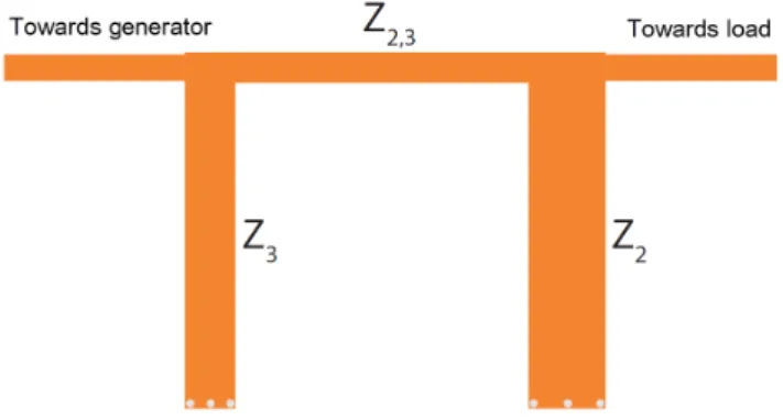
Fig. 1. Third order matching network withλ/4shorted stubs.
The impedance values are the reciprocal, of the given admittances respectively (Z2, Z3, Z2,3). The third-order match- ing network structure is shown in Fig. 1. However, this method does not always provide purely real transmission line impedance values. In several cases, if the input parameters are not well chosen the equations may lead to complex trans- mission line immittances. Complex transmission lines are not realizable with lossless components. For effective impedance matching, only lossless circuit elements are allowed (with purely real impedance values), otherwise the required power would not reach the load, but dissipate in the lossy elements.
In the following section mandatory parameter restriction is presented, used for avoiding these unwanted complex trans- mission line impedances.
IV. AVOIDING COMPLEX TRANSMISSION LINE IMPEDANCES
Matching network transmission line impedances are ex- pressed as the reciprocal of the admittance values. As known from linear network theory, these impedance values can be solely purely real (assuming lossless transmission lines). How- ever there are multiple cases where the results are complex impedance values. Complex impedance value may arise first during the design if
Im(J2,3)= 0. (28)
It is also worth mentioning that J2,3 can be purely real, or pure imaginary due to the nature of the square root function, in (24). In order to avoid the pure imaginary impedance value it is necessary to point out which parameter values affect this.
If
C2C3
g2g3 <0, (29)
then J2,3 is pure imaginary. As the parameters are multiplied together, an odd number of negative coefficients in the ex- pression can result in a value less than zero. Due to the fact that the decrementδ, and Green-coefficientsk1,2 andk2,3 are always greater than or equal to zero, g0,g1, andg2 can only be positive. Thus a negative value in Eq. (29) can solely occur
ifC3<0, leading tog4<0. Theg4parameter is negative if, D <0, resulting
D <0 iff. d δ sin π
2n
<1, (30)
assuming that n = 3 (third-order matching network) and δ >0:
Im J2,3
= 0 iff. 2d > δ. (31) In order to avoid complex transmission line impedance values, the mandatory rule is to set,
d > δ
2. (32)
On one hand the d parameter can be set by modifying r, which stands for the amount of allowed Chebyshev-ripple in the matched frequency band, on the other hand the decrement factor (δ) is pre-determined by the quality factor, and the frequency band. If the matching task allows the modification of eitherr, or flandfh, this mandatory rule can be satisfied (in some cases), as shown later in Section VIII-B.
V. PHYSICAL TRANSMISSION LINE IMPEDANCE LIMITATIONS
As most of the matching circuit designs are based on microstrip transmission lines, one should always avoid extreme line impedances. As a basic rule e.g. on a printed circuit board, transmission line impedances should be15 Ω≤Z ≤150 Ω.
This is due to the copper structure manufacturing tolerance limits. The matching network realization fails, if any of these transmission line impedances do not obey this rule. As an example let’s assume a purely realZ2,3 that satisfies the rule
15 Ω< RL g2g3
C2C3 <150 Ω. (33) Substituting into this expression,
RL
g2g3
C2C3 =RL
D Rgk1,22
RLk22,3 , (34) where RL is the real part of the load impedance, and Rg is the generator impedance. If the condition,
15 Ω< RL
D Rgk1,22
RLk22,3 <150 Ω, (35) does not apply, the matching network is not realizable, due to the aforementioned physical limits. This short expression requires only five parameters, and can be used to exclude non- realizable matching networks at an early phase of the network design. The same limit calculation can be applied toZ2 and Z3, however the expression is more complex, and irrelevant, considering the fact, that if at least one of the transmission line impedances is not realizable, the matching network is non- realizable as well.
Algorithm 1Modified matching algorithm task→initial parameters(RL, Rg, L, fc, b, r) while|S11|>−10dBdo
calculatedandδ parameters if2d > δthen
non-complex matching network calculateD, k1,2, k2,3
if15 Ω< RL
D Rgk21,2
RLk22,3 <150 Ωthen
physically realizable, non-complex network calculate network impedances(Z2, Z3, Z2,3) recalculate|S11|
else
physical realization problem, modifyr orb end if
elseif2d < δ then
complex matching network, modifyr orb end if
end if end while
successful matching is achieved
VI. ALGORITHMIC IMPLEMENTATION OF THE MODIFIED MATCHING METHOD
A modified matching algorithm (Algorithm 1) is defined herein for avoiding the non-realizable matching network solu- tions, by using the rules given in previous sections. As it can be seen in Algorithm 1, the matching network impedances should only be calculated, if both physical limitations are satisfied.
The complexity of these calculations can be further reduced, if the calculation of parametersdand δ is faster. The aim of the upcoming section is to show a possible faster approximate expression to calculate the required parameterdfromr, thus speeding up the iteration process.
VII. SIMPLIFIED CALCULATION OF THEdPARAMETER
The exact calculation of the parametersdandDfor Green’s coupling coefficients were shown in Section III. As the hyper- bolic, and the inverse hyperbolic functions may be difficult to evaluate, this paper will introduce a simplified approximate expression for the parameterd. As
sinhx= ex−e−x
2 , (36)
sinh−1x= ln x+
x2+ 1
, (37)
these expressions can be used to transform hyperbolic equa- tions to their exponential and logarithmic forms. By substitut- ing
u=
1
10(r/10)−1,
the parameterd can be rewritten in the form:
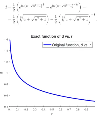
d= 1 2
eln(u+√u2+1)13 −eln(u+√u2+1)−13
=
= 1 2
3
u+
u2+ 1
−1 2
3
u+
u2+ 1 −1
.
0 0.1 0.2 0.3 0.4 0.5 0.6 0.7 0.8 0.9 1
r
0.4 0.6 0.8 1 1.2 1.4 1.6
d
Exact function of d vs. r
Original function, d vs. r
Fig. 2. The original function ofdvs.r
0 0.1 0.2 0.3 0.4 0.5 0.6 0.7 0.8 0.9 1
r
0.4 0.6 0.8 1 1.2 1.4 1.6
d
Exact and approximate function of d vs. r
Approximate function:
Original function, d vs. r Approximate function
Fig. 3. The original and the approximate function ofdvs.r
As can be seen from Fig. 2, ifdvs.ris plot in the Carte- sian coordinate-system, the function resembles a monotonic decending hyperbolic function. These embedded square, and third-root functions are computationally extensive, thus an ac- ceptable approximate function is proposed. The approximation (i.e the curve fitting task) was carried out in MATLAB 2017b.
As mentioned before the proposed initial function is a custom hyperbolic function which has the symbolic form
d(r) =ˆ 1 a·rb+c,
Overcoming the Realization Problems of Wideband Matching Circuits INFOCOMMUNICATIONS JOURNAL
INFOCOMMUNICATIONS JOURNAL, 2018 5
wherea,b,care arbitrary constants. Utilizing the Least-Square Method based curve fitting, these constants were determined
a= 0.618, b= 0.1118, c=−1.1233.
Based on these constants, the approximate function fordis d(r) =ˆ 1
0.618·r0.1118 −1.1233. (38) This approximate and the original exact function is presented in Fig. 3. The curve-fitting approximation exhibited acceptable results, with an RMSE (Root Mean Squared Error) value of 8.86·10−4, and R-square factor of1.00. On this basis it can be safely stated that
d≈ 1
0.618·r0.1118 −1.1233. (39) During the iterative solution to the best matching network, in Algorithm 1 the parameter d should be reevaluated as soon asr changes. This evaluation occurs everytime the algorithm runs into an unrealizable matching solution. With this new hyperbolic formula introduced here in Eq. (39), the resulting algorithm exhibits a reduced processing time.
VIII. MATCHING EXAMPLES(SIMULATIONS) In this section two matching examples are introduced. One where the2d > δcondition is initially satisfied, and another where it is not. These simulation setups were created inAWR Microwave Design Studio 2010. The simulated impedance matching networks are designed for matching series R-L loads to a Rg = 50 Ωgenerator, on a specific European ISM UHF frequency band, i.e. 868 MHz.
A. Impedance matching example 1.
The impedance matching example parameters are shown in Table I,
TABLE I
IMPEDANCE MATCHING EXAMPLE1. -INITIAL PARAMETERS
fc b Rg RL L r δ d
868 MHz 25% 50Ω 30Ω 20 nH 0.066 0.5366 1.068
where values in bold, are parameters calculated from the six initial parameters: center frequency, relative matching bandwidth, generator source impedance, load resistance, load inductor value, and maximal Chebyshev-ripple factor respec- tively. Regarding the values in Table I, the fundamental rule for non-complex transmission line impedances (presented in Section IV.) and the practical impedance realization limit are both satisfied (see Eq. (35)).
The matching network consists of the following transmis- sion line impedances, and series capacitance.
Fig. 4 presents the input reflection coefficient as a function of frequency, for the matching network. As it is highlighted with the markers, an acceptable matching (|S11| ≤ −10dB) is reached on the 738. . .1116MHz frequency band. The physical line impedance realization limit is satisfied as well,
15 Ω<50√
1.153<150 Ω.
Fig. 4. Wideband matching result, for example 1.
TABLE II
MATCHING NETWORK COMPONENT PARAMETERS(EX. 1.)
Z2,3 Z2 Z3 Cseries
51.36 Ω 26.75 Ω 70.9 Ω 1.68pF
As a conclusion, this example clearly states, that by abiding the rules introduced in Section IV. and Section V. one can avoid matching networks that are practically impossible to implement.
B. Impedance matching example 2.
In this example the initial parameters donotsatisfy the fun- damental realization rule (see Eq. (32)), therefore resulting in a non-realizable matching network. Overcoming this problem is presented hereby.
TABLE III
IMPEDANCE MATCHING TASK2. -INITIAL PARAMETERS
fc b Rg RL L r δ d
868 MHz 10% 50Ω 50Ω 20 nH 0.066 2.281 1.068
One might presume, that this matching task is easier, due to the smaller bandwidth, and higher real part of the load impedance, however the Bode-Fano method basically does not respect the realization rule shown in Section IV., hence the synthesis results in complex transmission line impedances.
TABLE IV
MATCHING NETWORK COMPONENT PARAMETERS(EX. 2.)
Z2,3 Z2 Z3 Cseries
−18.86jΩ 7.31 + 3.472jΩ −1.21 + 0.0668jΩ 1.68pF
The solution for this problem is to either modify the matched relative bandwidth, or the Chebyshev-ripple factor, if allowed. This time, by settingr= 0.0001 the results have become acceptable (Fig. 5).
Balázs Matolcsy was born in Budapest, Hungary, in 1992. He received his B.Sc. and M.Sc. degree in Electrical Engineering at the Budapest University of Technology and Economics in 2015, and 2017 respectively. He joined the Department of Broadband Infocommunciation and Electromagnetic Theory in 2017 as a Ph.D. student. In 2018, he received a Short Term Research Scholarship from DAAD at the Technical University of Karlsruhe (KIT) in Germany. The main area of his research interests are high-frequency RF simulation, antenna design, visible light communication and mixed signal electronics.
Attila Zólomy received his M.Sc. and Ph.D.
degrees in 1994 and 2004, respectively, from the Budapest University of Technology and Economics in Electrical Engineering. He works currently at the university as a part-time researcher. He also works as a senior member at Silicon Laboratories Ltd. in Hungary. His main interest are the microwave and millimeter wave circuits, small antennas, impedance matching, RF Integrated Circuits and module design in the UHF and 2.4 GHz frequency bands. He is author and co-author of more than 60 scientific papers and application notes and mulitple accepted U.S. patents.
TABLE V
MODIFIED NETWORK PARAMETERS(EX. 2.)
Z2,3 Z2 Z3 Cseries
53.17 Ω 27.18 Ω 104.1 Ω 1.68pF
By modifying r,d is also modified (d = 3.668) and Eq.
(32) is thereby satisfied, thus the matching task is solvable exclusively utilizing lossless components (impedance values are in Table V). The results in Fig. 5 show that the matching quality is better than expected, and the matched bandwidth is almost 50%, contrary to the predefined b = 10%. This result is due to the outstandingly low, maximal Chebyshev- ripple factor, prescribed as the fix for avoiding complex impedances. As seen in this second matching example varying the Chebyshev-ripple factor has beneficiary effects on avoiding transmission line impedances. If the matching task allows, modifying the upper and lower frequency limits may have the same effect on avoiding unrealizable networks.
Fig. 5. Modifyingr factor results in successful impedance matching and realizable network
CONCLUSION
The presented physical realization problems and solutions introduced in Section IV. and Section V. were successfully validated with simulation examples. The modified wideband matching algorithm was presented, and successfully applied for multiple matching tasks. If the realization limiting equa- tions presented in this paper are satisfied, avoiding non- realizable matching networks becomes possible before com- plex calculations and optimalization steps were made. Fur- thermore the approximation for the parameter d reasonably reduces the calculation time at the iterative stage, thus speed- ing up the complete matching process.
ACKNOWLEDGMENT
The authors would like to acknowledge the financial support of the German Academic Exchange Service (DAAD).
REFERENCES
[1] R. M. Fano, ”Theoretical limitations on the broadband matching of arbitrary impedances”, J. Franklin Inst., Vol. 249, pp. 57-83, 1950.
[2] H. W. Bode, Network Analysis and Feedback Amplifier Design, Van Nostrand Reinhold Publishing Co., 1945.
[3] W. K. Chen, Broadband Matching Theory and Implementations, Third Edition, World Scientific Publishing Co. Ltd., 1993.
[4] W. K. Chen and C. Satyanarayana, ”General theory of broadband match- ing”, IEEE Proceedings Electronic Circuits and Systems, Vol. 129, No.
3, p. 96, 1982.
[5] Herbert J. Carlin, Pier Paolo Civalleri, Wideband Circuit Design, CRC Press, 1997.
[6] R. Kopru, C. Aydin, D. C. Atilla, C. Karakus and B. S. Yarman,
”Wideband matching network design for a V-shaped square monopole an- tenna using Real Frequency Technique”, 13th Mediterranean Microwave Symposium (MMS), 2013.
[7] Darlington S., ”Synthesis of reactance 4-poles”, Jour. Math. Phys., Vol.
XVIII., pp. 275-353., September 1934.
[8] Cuthbert T. R., Circuit Design Using Personal Computers, NY: John Wiley Publishing Co., 1994.
[9] G. Matthaei, ”Synthesis of Chebyshev Impedance-Matching Networks, Filters, and Interstages”, IRE Transactions on Circuit Theory, Vol. 3, No.
3, pp. 163-172., 1956.
[10] G. Matthaei, L. Young, and E. M. T. Jones, Microwave Filters, Impedance Matching Networks, and Coupling Structures, NY: McGraw- Hill, 1980.
[11] Youla D. C, ”A new theory of broadband matching”, Defense Technical Information Center, pp. 30-50., 1964.
Bal´azs Matolcsy was born in Budapest, Hungary, in 1992. He received his B.Sc. and M.Sc. degree in Electrical Engineering at the Budapest University of Technology and Economics in 2015, and 2017 respectively. He joined the Department of Broadband Infocommunciation and Electromagnetic Theory in 2017 as a Ph.D. student. In 2018, he received a Short Term Research Scholarship from DAAD at the Technical University of Karlsruhe (KIT) in Germany. The main area of his research interests are high-frequency RF simulation, antenna design, visible light communication and mixed signal electronics.
Attila Z´olomyreceived his M.Sc. and Ph.D. degrees in 1994 and 2004, respectively, from the Budapest University of Technology and Economics in Electri- cal Engineering. He works currently at the university as a part-time researcher. He also works as a senior member at Silicon Laboratories Ltd. in Hungary.
His main interest are the microwave and millimeter wave circuits, small antennas, impedance matching, RF Integrated Circuits and module design in the UHF and 2.4 GHz frequency bands. He is author and co-author of more than 60 scientific papers and application notes and mulitple accepted U.S. patents.