Journal Pre-proofs
Full Length Article
Evaluation of AES depth profiles with serious artefacts in C/W multilayers A.S. Racz, Z. Fogarassy, P. Panjan, M. Menyhard
PII: S0169-4332(21)03403-6
DOI: https://doi.org/10.1016/j.apsusc.2021.152385
Reference: APSUSC 152385
To appear in: Applied Surface Science Received Date: 7 September 2021 Revised Date: 21 December 2021 Accepted Date: 28 December 2021
Please cite this article as: A.S. Racz, Z. Fogarassy, P. Panjan, M. Menyhard, Evaluation of AES depth profiles with serious artefacts in C/W multilayers, Applied Surface Science (2021), doi: https://doi.org/10.1016/j.apsusc.
2021.152385
This is a PDF file of an article that has undergone enhancements after acceptance, such as the addition of a cover page and metadata, and formatting for readability, but it is not yet the definitive version of record. This version will undergo additional copyediting, typesetting and review before it is published in its final form, but we are providing this version to give early visibility of the article. Please note that, during the production process, errors may be discovered which could affect the content, and all legal disclaimers that apply to the journal pertain.
© 2021 Published by Elsevier B.V.
Evaluation of AES depth profiles with serious artefacts in C/W multilayers.
A.S. Racz †, Z. Fogarassy†, P. Panjan§, M. Menyhard†x
† Institute for Technical Physics and Materials Science, Centre for Energy Research, Konkoly Thege M. út 29-33, H-1121 Budapest, Hungary
§ Jožef Stefan Institute, Jamova 39, 1000 Ljubljana, Slovenia
ABSTRACT
Ion beam mixing was applied to produce tungsten carbide nano-layers in C/W nano-multilayer structures, which was studied by Auger electron spectroscopy depth profiling. The destructive AES depth profiling caused serious artefacts such as tungsten-carbide production at the interfaces, even when choosing the optimal sputter removal conditions. Here we show that ion mixing due to the AES depth profiling could be described by TRIDYN simulation, and compound formation could be also estimated by introducing a simple model. Thus, despite the serious artefact production the original pristine depth distribution could be reconstructed. This evaluation method has been checked on C/W layer systems containing tungsten-carbide enrichment in the interface region (due to high energy ion beam mixing); the true in-depth distribution could be reconstructed.
It has been found also that with increasing carbide formation the artefact production decreases allowing the use the AES depth profiling without reconstruction.
KEYWORDS: multilayers, tungsten-carbide, WC, coating, AES depth profiling, TRIDYN
1. INTRODUCTION
The applications of thin (thickness range of some nms) film systems are wide spread in semiconductor industry, biomedical implants and sensorics. Multilayer structures play an important role in the design of optical [1] tribological [2], corrosion resistant [3] and biomedical [4] coatings. The quantification of these structures can be carried out using cross sectional TEM, ellipsometry, XPS and AES depth profiling etc. All these methods have their specialties. Cross sectional TEM is excellent for the determination of the structures of thin film systems but it is rather expensive not to mention that retrieving chemical information is not always straight-forward and that typically the information originates from an extremely small volume. Ellipsometry is fast
and cheap, however, in the case of thin multilayer systems the interpretation of the results is far from evident and receiving information concerning chemical changes is especially difficult. The XPS and AES depth profiling techniques are relatively cheap, they can handle thin multilayer structures with depth resolution in the range of nms, giving reliable chemical information. They are characterizing a relatively large area, however these depth profiling techniques are destructive methods. In both cases ion bombardment is used to remove the material which might introduce serious alterations, like bombardment induced morphology development [5], ion beam mixing (IBM) [6], radiation induced diffusion [7], compound formation [8], amorphization [9] etc. to the studied samples. A great deal of effort has been invested to optimize these methodologies by developing both the experimental hardwares (minimizing the introduced damage) and the reconstruction softwares (making corrections for the evaluation of the measured depth profiles).
The most important hardware optimization of AES depth profiling was the introduction of the Zalar rotation [10] resulting in reasonable low surface roughening. The Zalar's group also realized that using two ion guns simultaneously [11] results in the reduction of surface roughening, as well. Our group introduced the grazing angle of incidence ion beam sputtering method which reduces the surface roughening and IBM [12]. Further development was lowering the energy of the bombarding ions which also contributes to the diminution of IBM. It should be admitted, however, that even with all these hardware developments, still a damaged (the extent of which strongly depends on the chemical composition of the sample) surface will be studied, thus the recorded Auger spectra originate from a distorted region. Moreover, one should also realize that the information depth of AES is some nm-s and thus, the measured signal reflects an average of the composition in the surface close region. Thus, for the optimal use of the method refined, evaluation methods are to be applied. These are mainly trial and error type of methods: an in-depth concentration distribution is assumed and considering the ion beam damage and the mechanism of Auger electron emission the Auger currents are calculated. Then the in-depth distribution assumptions are varied until the measured spectra are sufficiently reproduced. One of the frequently used such algorithms is the Mixing-Roughness-Information depth- (MRI) method [13–
17], which considers ion bombardment induced mixing, roughening, preferential sputtering and it also corrects the results for non-zero inelastic mean free path (IMFP). This method applies analytical functions for describing the various processes. We have developed an alternative approach. The ion bombardment induced alterations, ion beam mixing and preferential sputtering,
can be simulated by means of TRIDYN code [17, 37], while the bombardment induced roughness is handled similarly as by MRI, by applying a Gaussian convolution. The Auger signal is calculated using a layer model, taking into account the change of IMFP in the intermixed region [19].
In this paper we will report on the application of this method for the depth profiling of layer systems containing carbon and tungsten layers. For such samples we know that using medium energy ion bombardment for ion beam mixing a fair amount of mixing and compound formation (e.g. carbide) occurs. While the latter is a definite advantage from application point of view (in fact it is used for producing corrosion resistant nano-coating layer [20–22] it might be disadvantageous from the depth profiling point of view. In fact, already at 1 keV ion sputtering, compound formation along the interfaces occurs, strongly affecting the shape and intensity of the Auger peaks which makes the evaluation even more complicated. Nevertheless, we will show that our modified evaluation routine can be applied for the evaluation of these depth profiles. It is obvious that the reconstruction of the experimental in-depth profile becomes more challenging in case of greater damages. Thus, first we will determine those parameters of ion sputtering which minimize the alteration of the studied specimen. The aim of this article was twofold: firstly a method will be shown for handling the ion sputtering induced alteration during depth profiling of pristine C/W.. structures, secondly we will check how the low energy ion sputtering affects the tungsten-carbide/C and W interfaces by using the same evaluation method.
2. EXPERIMENTAL SECTION
2.1. Sample preparation
A C/W/C multilayer structure was produced by sputter deposition using a Si single crystal substrate. The sputtering was performed in a Balzers Sputron sputtering chamber in Jožef Stefan Institute, Ljubljana. A plasma beam (typically 40 V/40 A) was produced between the hot filament and the auxiliary anode around the target. The pyrolitic graphite and the tungsten (99.99%) targets with a diameter of 60 mm are interchangeable in situ. The sputtering voltage was held constant at 1700 V with 0.6 A of target current. The substrates were away from the plasma therefore it was possible to keep the substrate temperature during deposition process below 100 °C. The thickness of the sputtered layer was controlled by quartz-crystal microbalance.
For producing carbide-rich nano-layers by IBM the C/W/C/Si substrate samples have been irradiated by xenon ions in Helmholtz Zentrum Rossendorf Dresden in a High Voltage Engineering Europa B.V., Model B8385 implanter (see Acknowledgement). The ion energy was 40 and 120 keV, the fluences were 2.5 x 10¹⁵ Xe+/cm2 and 5 x 10¹⁵ Xe+/cm2, respectively.
2.2. TEM studies
The initial structure of the specimens was determined by cross sectional transmission electron microscopy (XTEM). The XTEM measurements were performed in a FEI-Themis (scanning) transmission electron microscope (STEM) with a Cs corrected objective lens, in HRTEM (High Resolution Transmission Electron Microscope) mode (point resolution is around 0.07 nm) operated at 200 kV.The sample preparation for XTEM was made by FIB ion milling.
The actual thickness for the layer system was found to be C 10.4 nm / W 24.5 nm / C 9.1 nm. For easier reference we call the samples as 102010.
2.3. AES depth profiling
As it was mentioned the key issue in using AES depth profiling is to find the best conditions for the ion removal process; first we will deal with this question.
2.3.1. Choosing the conditions of ion sputtering.
Our standard ion bombardment conditions, which results in better than 1 nm depth resolution for many samples are, 1000 eV Ar+ with angle of incidence 80o (with respect the surface normal) and rotated specimen [12]. The grazing angle of incidence was introduced to minimize the surface roughening and ion mixing mentioned earlier. In the cases of C/W/C... systems, using the usual parameters for AES depth profiling the results were discouraging; the relative sputtering yield ratio, rc/rw, was found to be ~ 4.7 a difference far greater than those that could be handled by any software solution. Thus one must find some lower value. There are databases [23,24] containing sputtering yield data, however just in the range of grazing angle of incidence they are not too reliable. Similarly SRIM data [25] are also available but similarly their reliability is also poor in the grazing angle of incidence range [26]. Therefore, the dependence of the sputtering yield ratio on the angle of incidence had to be checked experimentally. Since the thickness of the intermixed
region and the bombardment induced roughening increases with decreasing angle of incidence, an optimum had to be found. In our case this optimal angle of incidence was found to be 65o. The as recorded AES depth profile, applying this angle of incidence, is shown in Fig.1.
Fig.1. The as recorded AES depth profile of sample 102010. Sputtering conditions: 1keV, Ar+, 65o angle of incidence, rotated sample.
The experimentally measured sputtering yield ratio, rc/rw, at 65o angle of incidence is 1.71. The SRIM calculation predicts somewhat lower value of rc/rw =1.51. Though this angle is far from optimal from the point of view of sputtering induced roughening, we did use it since in the case of amorphous layers the sputtering induced roughening is not too severe.
2.3.2. Measurement of AES depth profiles
The Auger spectra were recorded by a STAIB DESA 150 pre-retarded Cylindrical Mirror Analyzer (CMA) in direct current mode. For the depth profiling 1 keV Ar+ ions were used with an angle of incidence of 65° with respect to the surface normal. The ion current was kept constant during sputtering. The sample was rotated (6 rev/min) during ion bombardment.
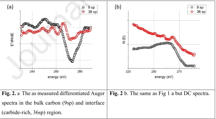
The shapes and energies of the CKLL Auger peak in carbide and graphite phases are different. Fig.
2 shows two as recorded differentiated (AC) (a) and non-differentiated (DC) (b) Auger spectra obtained on 102010 pristine sample in the graphitic, 9th spectrum, and carbide rich, 36th spectrum, regions, respectively. In both measurement modes the curves are strongly different. For the determination of the actual compositions various decomposition methods can be used. We have applied the CasaXPS program [27], which uses the DC spectra (shown in Fig 2b). In this case the measured spectra are fitted with references by applying linear least square solution (LLS). Carbide reference spectrum was taken from a measurement where pure WC region was produced due to IBM. The graphite reference was taken from the pristine sample where pure carbon layer was present. After the decomposition for calculating the areas of the sub-peaks Universal Tougaard background was used. The relative sensitivity factor method [28] was applied for the calculation of the concentrations. The relative sensitivity factors for C and W were determined from the intensities measured on pure C or W layers. The relative sensitivity factors for C emitted from WC (tungsten-carbide) were determined from a sample where pure tungsten-carbide phase was produced by the IBM. For xenon such sensitivity factor was chosen which provided the implanted fluence in the case when all the bombarding projectiles remain in the sample; its maximum concentration was 3 at%. Hence the AES analysis provided the atomic fraction of graphitic C, metallic W, WC, metallic Si and the bombarding projectile as a function of sputtering time.
Fig. 2. a The as measured differentiated Auger spectra in the bulk carbon (9sp) and interface (carbide-rich, 36sp) region.
Fig. 2 b. The same as Fig 1 a but DC spectra.
Fig. 1 showed that the AES intensity of C emitted from the first (pure) carbon is larger than that of the second (pure) carbon layer. Similarly, the AES intensity of the pure W layer decreases with increasing depth. These changes are explained by strongly different backscattering factor of the elements involved; the backscattering factors of the light Si and C is about 40% less than that of the heavy tungsten. The precise calculation of the varying backscattering factor is difficult [19].
In this work as a rough approximation we have simply varied the relative sensitivity factor along the depth.
The sputtering time was transformed to the removed layer thickness by applying our previously elaborated method [29]. It´s summary is as follows. The relative sputtering yields of pure C and W could be determined from the sputtering times required to remove the known layer thicknesses of the as-deposited W and C layers. In the regions that contain mixed C and W components (independently from their chemical state) we suppose that the total sputtering yield Y can be estimated as Y = XCYC +XWYW where Yi and Xi are the sputtering yield and concentration of component i (in our case ’C’ or ’W’). All presented in-depth distributions were calculated by this procedure.
2.4. Simulation of AES depth profiling 2.4.1. Ion beam mixing
The AES depth profiling was simulated by means of TRIDYN code [37]. The code considers a one dimensional material which is built up by layers, the thickness of which is determined by the user. For simulating the depth profile in the pristine sample we built a structure which consisted of pure C, W and Si layers separated by abrupt interfaces with thicknesses according to the XTEM results. Then the sample was subjected to ion bombardment applying exactly the same conditions (1 keV Ar+, 65º) than that used in the experiment. The concentration distributions were recorded in predetermined steps, thus the output provides the concentration distribution of the elements along the depth. This process is repeated until all of the layers are removed from the Si substrate.
Having the concentration distributions we can calculate the emitted Auger intensities using the exponential decay law. The IMFP values for elements were taken from [30]. For the intermixed regions the IMFP was calculated by the usual approximation 1/=Xi/i where Xi is the concentration. Having the Auger intensities, the concentrations can be calculated using the same
expression as in the experiments. The compound formation is now calculated by using the simple assumption (details see later) that all minority components W or C form carbide. This simulation and calculation procedure leads to the simulated depth profile (concentrations of elements and carbide compound along the depth) which is then compared with the experimental one.
As the TRIDYN calculation is one dimensional it cannot deal with the interface roughening. If interface roughening is present and its wavelength is not in the nanoscale, then it can be approximated by a rectangular structure. The simulation is performed for all columns and the results are averaged, providing a fair estimate of the effect of the roughness. Besides the concentration distributions, the code also provides the total and partial sputtering yields during the depth-profiling process, and the surface recession (removed layer thickness).
The procedure for simulating the depth profiles of samples modified by IBM (applying xenon irradiation) differs partly from the above description. An input layer structure is supposed which is depth profiled with TRIDYN as described above. If the simulated profile and the experimental one do not fit the input layer structure is changed until a good agreement is not provided. That input layer structure which provided the good agreement is the one which was produced by the IBM.
2.4.2. Compound formation
The approach for calculating the WC compound formation was similar to that used in the case of the ion mixing of Si/C system [21,31]. The basic assumption is that the compound formation can only take place in the intermixed region. Thus, we may assume that first intermixing happens and then if favorable conditions met compound formation takes places in the intermixed region.
One of the conditions which is to be met is that the two atoms to be reacted should be first neighbors being in crystalline or interstitial positions. At the beginning of the mixing process the A recoils enter to nearly pure B matrix and vice versa, and the neighbors are automatically B or A atoms; thus the requirement being on nearby sites at the beginning of the mixing process is met.
When the amount of the compound increases the probability that the excited recoils meet an unlike atom decreases, this reduces the rate of compound formation. E.g. based on experimental observations in the case of C/Si system the highest amount of carbide concentration which could be reached was around 80% [20]. Thus, for the C/Si case, we used a compound formation model, which assumed that all minority atoms form carbide if the carbide concentration is less than 80%
This model worked properly in a wide range of irradiations and sample structures ranges [20–
22,32]. In the present case the situation seems to be more complex. In the majority of the cases the experiments revealed regions where the WC concentration was 100 % and was accompanied either C or W. This cases can be described well in the simulation by assuming that all minority elements form carbide. In few cases we have found regions where WC concentration was in the range of 85-95% and besides the tungsten-carbide non-reacted W and C was also found (see Fig.8 b) as well. The concentration of the minor component of the non-reacted W and C was always lower than 10%. Since the number of these regions was low we will ignore them and will assume that all minority atoms form carbide. This way the tungsten-carbide concentration might slightly be overestimated close to the saturation value.
3. RESULTS AND DISCUSSION
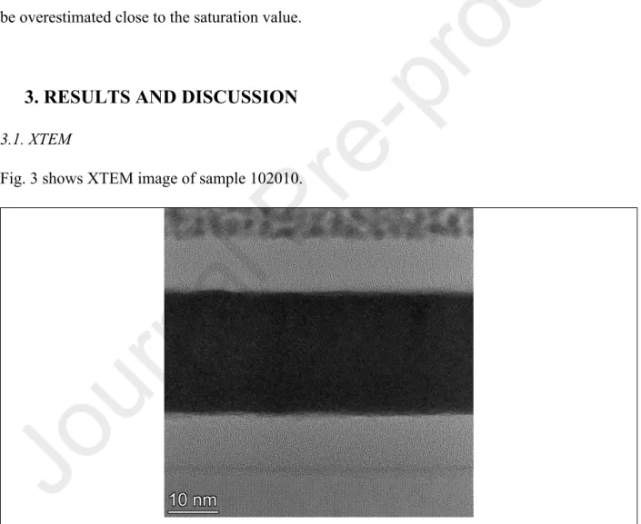
3.1. XTEM
Fig. 3 shows XTEM image of sample 102010.
Fig. 3. The XTEM image of pristine 102010 sample.
At the bottom of the picture the crystalline Si substrate can be seen, which is covered by the amorphous carbon and tungsten layers. The image clearly shows that all interfaces are sharp and straight. The interface roughness was estimated to be less than 1 nm.
3.2. AES depth profiling & simulation
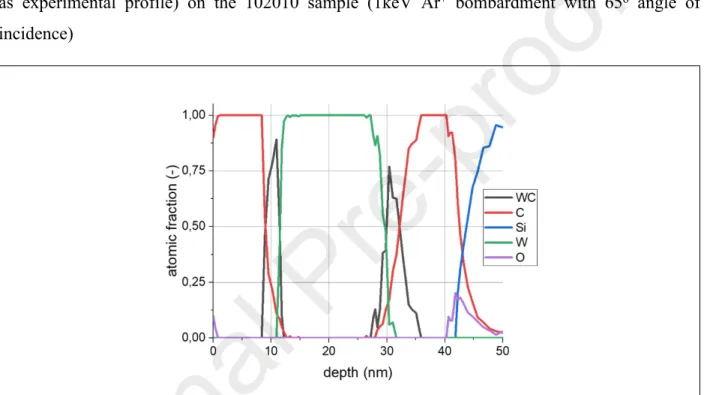
Fig. 4 shows the depth profile derived from the measured peak-to-peak values (later called as experimental profile) on the 102010 sample (1keV Ar+ bombardment with 65o angle of incidence)
Fig. 4. The experimental AES depth profile of pristine sample 102010. Sputtering conditions: 1 keV Ar+, angle of incidence 65º with respect to the surface normal.
The depth profile clearly shows the layer structure and the slight oxygen contamination of the silicon substrate, which is expected. On the other hand, there is an unexpected striking feature in Fig.4; it is the appearance of the WC layers. Both the C/W and W/C interfaces disappeared and the layers are separated by WC layers. The shape and extent of the carbide layers (see later Fig. 6 a and b) are different on the crossing from the carbon layer to the tungsten and vice versa. The TEM image excludes the presence of such layers in the pristine 102010 sample, thus the
appearance of the WC is due to the depth profiling procedure and thus it is a serious artefact of the method. In the following we will try to understand the observed features.
3.2.1. C/Si interface
The evaluation of the depth profile obtained from this region seems to be the easiest since in this region carbide formation due to the material removal did not occur [33] and thus, this interface can be used to check the sputtering induced interface roughening. To get information on interface roughening the depth profiles based on Auger peak of SiLVV (92 eV) was measured and simulated. The inelastic mean free path (IMFP) of SiLVV Auger electrons is 0.5 nm [30], which provides an excellent depth resolution.
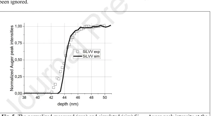
Fig 5. shows the normalized measured and simulated Auger depth profiles based on the SiLVV
Auger electrons in the C/Si (substrate) interface region. The simulation assumed according to the TEM result a sharp step function C/Si interface; the presence of slight oxygen contamination has been ignored.
Fig. 5. The normalized measured (exp) and simulated (sim) SiLVV Auger peak intensity at the C/Si (substrate) interface region.
It is clear that there is a difference between the measured and simulated curves in the 42- 44 nm depth region, meaning that the assumption of initial step function for C/Si transition does
not work; there is some interface roughness of 1-2 nm. This small roughness might be because of a./ ion bombardment induced mixing, b./ ion bombardment induced roughening. In any case the observed roughness is small enough. Assuming that the broadening is due to interface roughening we can make a fair estimate on the upper limit of interface roughening on the W/C2 interface as well, based on the method of Barna [34]. It tells that the bombardment induced roughening scales with the thickness of the removed layer. The carbon layer is amorphous which is not sensitive for ion bombardment induced roughening. Its thickness is only 9.1 nm. Thus, the sputter removal of this layer conserves the initial roughness meaning that the interface roughness at the W/C2 interface cannot be more than 1-2 nm. This way we conclude that there is no serious ion bombardment induced roughening during the removal of the layers even using this unfavorable low angle of incidence. Therefore, in the following the ion bombardment induced roughening will be ignored and will be not included in the simulation procedure.
3.2.2. C/W and W/C interface regions
The study of this interface is more difficult than that of the previous one since here, besides the IBM compound formation also occurs. Fig. 6. shows the comparison of the experimental AES depth profiles at the C/W and W/C interfaces with those of the simulated ones.
Fig.6. a. The distribution of WC at the C/W interface; experimental (exp) and simulated (sim) curves.
Fig.6. b. The same as Fig. 6 a but at the W/C interface.
It is clear that either the shapes of the measured depth profiles or the integrals (amount of WC) of the WC peaks (note that scales of Fig. 6a and Fig. 6 b are the same) at the C/W and W/C transitions are different. At the C/W transition at the C side the C drops suddenly to zero and the WC increases sharply, which is followed by a slower change, thicker transition layer on the W side. At the W/C interface, however, both transitions are wider and the amount of WC observed larger than that of at the C/W interface. It is known, that the A/B and B/A transitions at AES depth profiling might be different [35].
In the simulation based on the TEM images step function transitions at both C/W and W/C interfaces have been chosen for the starting distribution. Surprisingly the basic features of the experimental results are well represented by the simulation. At the C/W interface the sudden C drop is well fitted, while the rise of the WC is somewhat sharper for the simulation than that in the experimental results. The most important difference between the simulation and the experiment is the long penetration (tail) of the WC to the W metal layer. The situation is similar in the case of the W/C interface. Here the simulation nearly perfectly fits the experimental curves except the tail of the WC to the C layer, which seems to be even stronger than that in the case of the C/W interface.
Since the difference between the two interfaces are nicely reflected by the simulated one can conclude that the ion mixing mainly occurs by ballistic processes (our simulation considers only that). The actual surface concentration is strongly affected by the sputtering yield differences, which might explain part of the difference of the two interfaces. It is also clear that the simple model for the compound formation is also proper. Thus, we can determine from the figures (with the help of atomic densities) the amount of WC produced by the artefact being 122 and 176; 118 and 156 WC number/nm2 for the C/W and W/C transitions of the experimental and simulated curves, respectively.
The only problem with the simulation is the longer tail of WC to the next pure matrix than that of the experimental value. This difference might be due to non-ballistic processes. Previously we have observed that the post ion mixing processes might also work in systems susceptible for compound formation. E.g. in the case of Ni/C system post ion mixing segregation to the interface occurs producing a sharp interface[36]. We propose that similar process might be responsible for the sharper experimental shape of the WC. In any case the amount of WC in the tail is negligible
compared with that in the layer thus, it can be neglected. This also means that the method can be used for the estimation of the artefact production in any pristine C/W/C… type of systems.
3.3. AES depth profiles of ion beam mixed layers experimental & simulation
IBM produces WC in the W/C samples. Depending on the energy, ion type and fluence of the IBM various scenarios might be expected. At lower ion fluences and energies WC enrichment around the interfaces occurs, while increasing the ion energy and fluence these regions overlap and a finally a single WC region forms. We wish to use the AES depth profiling for studying such systems containing WC as well. Based on the previous prior to the application of the method it is important to check the nature of the artefact and to see if our method can handle the system.
First we will deal with a sample subjected to a high energy high fluence IBM; where the expectation is that all the tungsten transforms to tungsten carbide. The actual irradiation parameters are: 5 x 10¹⁵/cm2 Xe+ of 120 keV. Since the sample consists of 30% more C atoms than W atom after the complete intermixing some C remains and the expected structure is C/WC/C/Si. Fig.7 shows that the AES depth profile meets with this expectation. It indicates that the thickness of the WC layer produced is 30.6 nm.
Fig.7. The experimental (exp) and simulated (sim) depth profiles obtained from sample 102010 irradiated by 5x10¹⁵/cm2 Xe of 120 keV and the WC distribution (ini) chosen for the simulation.
The insert shows the sketch of the structure assumed for simulation.
For the simulation the same structure, C/WC/C/Si, was supposed and the best fit was reached by choosing a thickness of 29 nm for the WC layer. For all interfaces step function have been chosen. That is, the real thickness of the WC layer produced by the IBM is 29 nm. The experimentally measured value is 30.6 nm, which is only slightly larger than that of the initial value. Thus, for such structures a./ our method is applicable for the reconstruction of the initial structure from the measured depth profile b./ the experimentally determined thickness can be safely used for the determination of the IBM layer, c./ artefact production does not affect the results.
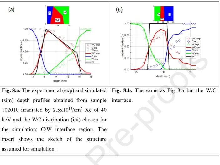
To check the robustness of our method, we will inspect the AES depth profile obtained from a sample subjected to a light IBM of 2.5x10¹⁵/cm2 Xe+ of 40 keV. The projected range of the 40 keV Xe ions in such a layer system is 13±3 nm [25].Thus in this case the expectation is that the majority of the IBM is concentrated on the first C/W interface while the second C/W is more or less untouched. Moreover, while around the interface there should be WC, the majority of the layer structure remains untouched. Fig. 8 a and b shows the measured depth profiles in the C/W and W/C regions. These only partly reflect the simple expectation. At the C/W interface region the WC reaches almost 100 % concentration at around 6 nm depth (thus high amount of C of the first C layer was transformed to WC) then the concentration slightly decreases up to a depth of 14 nm, then a sharp drop of WC occurs. The WC distribution at the W/C region seems to be simpler. It shows a distribution which is peaked at about the original interface and asymmetrically decreases toward to the originally pure W and C layers. The amount of WC is higher at the first C/W region than that in the second W/C region as is expected, while seems to be more than zero at the W/C interface which does not agree with the expectation.
Fig. 8.a. The experimental (exp) and simulated (sim) depth profiles obtained from sample 102010 irradiated by 2.5x10¹⁵/cm2 Xe of 40 keV and the WC distribution (ini) chosen for the simulation; C/W interface region. The insert shows the sketch of the structure assumed for simulation.
Fig. 8.b. The same as Fig 8.a but the W/C interface.
Let's not forget that in the case of pristine sample the experimentally found thicknesses of the WC layers were about 2 nm and 3 nm, for the C/W and W/C interfaces, respectively. These values are definitely lower than the measured thicknesses in Fig. 8 a and b. Thus, it is clear that IBM produced WC layers at both interfaces. Since the IBM was rather active in the region of the C/W transition, a thick layer with a structure of diffusional growth formed. In the simulation that WC distribution which provided the best fit between the measured and simulated curve agrees well with the measured curve. Thus, in this case one can use the experimentally measured distribution as the one produced by the IBM; obviously the artefact due to the depth profiling in this case does not affect the measurement.
At the W/C interface region the WC distribution which gives the best fit, that is the reconstructed WC profile, is considerably different from the experimentally measured WC distribution, showing that in this region serious artefact production occurs. In such cases we cannot rely on the measured depth profile for the determination of the amount of tungsten carbide produced by the IBM, but we should reconstruct the true profile by applying our method.
Based on these results we can accept the rule of thumb that in case of large intermixing and carbide formation the measured depth profiles provide safe estimates of the amount of carbide, while in case of slight IBM producing smaller amount of carbides simulation is required for the determination of the carbide content of the irradiated material. It also follows that in cases of thicker carbide the artefact production of the AES depth profiling can be neglected.
4. CONCLUSION
Serious artefact production of the AES depth profiling in the case of C/W multilayer system was observed; during depth profiling using usual ion irradiation conditions tungsten-carbide formation was detected. The amount of tungsten carbide produced was different on the C/W and W/C interfaces. It was shown that by using a TRIDYN based evaluation technique the interface dependent tungsten-carbide formation could be well described. The layer system was subjected to various ion beam induced mixing to produce tungsten-carbide nano-layers. By using the same evaluation technique, the WC distribution produced by IBM could be restored from the measured depth profile. It was also shown that the artefact production is less serious in the case of thicker carbides and it can be ignored in the evaluation.
AUTHOR INFORMATION
Corresponding Author
E-mail: menyhard.miklos@energia.mta.hu
ACKNOWLEDGEMENT
The EU H2020 Project No. 824096 “RADIATE”, HZDR-Dresden and project funding of Centre for Energy Research is highly acknowledged. Authors thanks the support of VEKOP-2.3.3-15- 2016-00002 of the European Structural and Investment Funds. This paper was supported by the János Bolyai Research Scholarship (Z. Fogarassy) of the Hungarian Academy of Sciences.
Authors are grateful for U. Kentsch for performing the ion irradiations. Thanks for A. Sulyok for providing AES facility. Guidance of N. Fairley in CasaXPS program is highly acknowledged.
Thanks are given for L. Illés for FIB lamella preparation.
REFERENCES
[1] C. Garlisi, E. Trepci, X. Li, R. Al Sakkaf, K. Al-Ali, R.P. Nogueira, L. Zheng, E. Azar, G.
Palmisano, Multilayer thin film structures for multifunctional glass: Self-cleaning, antireflective and energy-saving properties, Appl. Energy. 264 (2020) 114697.
https://doi.org/10.1016/j.apenergy.2020.114697.
[2] B. Liu, B. Deng, Y. Tao, Influence of niobium ion implantation on the microstructure, mechanical and tribological properties of TiAlN/CrN nano-multilayer coatings, Surf. Coat.
Technol. 240 (2014) 405–412. https://doi.org/10.1016/j.surfcoat.2013.12.065.
[3] N. Nemati, M. Bozorg, O.V. Penkov, D.-G. Shin, A. Sadighzadeh, D.-E. Kim, Functional Multi-Nanolayer Coatings of Amorphous Carbon/Tungsten Carbide with Exceptional Mechanical Durability and Corrosion Resistance, ACS Appl. Mater. Interfaces. 9 (2017) 30149–30160. https://doi.org/10.1021/acsami.7b08565.
[4] A.D. Pogrebnjak, C.-H. Kong, R.F. Webster, R.D. Tilley, Y. Takeda, K. Oyoshi, O.V.
Bondar, V.V. Buranich, S.V. Konstantinov, L.S. Baimoldanova, M. Opielak, P. Zukowski, P.
Konarski, Antibacterial Effect of Au Implantation in Ductile Nanocomposite Multilayer (TiAlSiY)N/CrN Coatings, ACS Appl. Mater. Interfaces. 11 (2019) 48540–48550.
https://doi.org/10.1021/acsami.9b16328.
[5] E. Chason, T.M. Mayer, Low energy ion bombardment induced roughening and smoothing of SiO 2 surfaces, Appl. Phys. Lett. 62 (1993) 363–365. https://doi.org/10.1063/1.108957.
[6] D. Leinen, A. Fernández, J.P. Espinós, J.P. Holgado, A.R. González-Elipe, An XPS study of the mixing effects induced by ion bombardment in composite oxides, Appl. Surf. Sci. 68 (1993) 453–459. https://doi.org/10.1016/0169-4332(93)90226-2.
[7] C. Chen, D.L. Green, E.L. Hu, J.P. Ibbetson, P.M. Petroff, Radiation enhanced diffusion of low energy ion‐induced damage, Appl. Phys. Lett. 69 (1996) 58–60.
https://doi.org/10.1063/1.118118.
[8] B.R. Chakraborty, Characterization of interfaces in nanoscale semiconductor devices by optimization of depth resolution in SIMS depth profiling, Appl. Surf. Sci. 221 (2004) 143–
154. https://doi.org/10.1016/S0169-4332(03)00875-4.
[9] N. Mottu, M. Vayer, R. Benoit, R. Erre, Is XPS combined with argon ion sputtering pertinent for depth profiling molybdenum-implanted stainless-steel layers?, Surf. Interface Anal. 34 (2002) 276–279. https://doi.org/10.1002/sia.1299.
[10] A. Zalar, Improved depth resolution by sample rotation during Auger electron spectroscopy depth profiling, Thin Solid Films. 124 (1985) 223–230.
https://doi.org/10.1016/0040-6090(85)90269-X.
[11] A. Zalar, S. Hofmann, Influence of ion energy, incidence angle and surface roughness on depth resolution in AES sputter profiling of multilayer Cr/Ni thin films, Nucl. Instrum.
Methods Phys. Res. Sect. B Beam Interact. Mater. At. 18 (1986) 655–658.
https://doi.org/10.1016/S0168-583X(86)80105-7.
[12] M. Menyhard, High-depth-resolution Auger depth profiling/atomic mixing, Micron. 30 (1999) 255–265. https://doi.org/10.1016/S0968-4328(99)00010-4.
[13] J. Kovač, A. Zalar, B. Praček, Quantification of AES depth profiles by the MRI model, Appl. Surf. Sci. 207 (2003) 128–134. https://doi.org/10.1016/S0169-4332(02)01331-4.
[14] S. Hofmann, H. Yang, J. Kovač, J. Ekar, Y.B. Song, J.Y. Wang, Artifacts in multilayer depth profiling: Origin and quantification of a double peak layer profile of Ag in ToF-SIMS
depth profiles of an Ag/Ni multilayer, Mater. Charact. 171 (2021) 110774.
https://doi.org/10.1016/j.matchar.2020.110774.
[15] S. Hofmann, G. Zhou, J. Kovac, S. Drev, S.Y. Lian, B. Lin, Y. Liu, J.Y. Wang, Preferential sputtering effects in depth profiling of multilayers with SIMS, XPS and AES, Appl. Surf. Sci. 483 (2019) 140–155. https://doi.org/10.1016/j.apsusc.2019.03.211.
[16] S. Hofmann, S.Y. Lian, Y.S. Han, Y. Liu, J.Y. Wang, Depth resolution and preferential sputtering in depth profiling of delta layers, Appl. Surf. Sci. 455 (2018) 1045–1056.
https://doi.org/10.1016/j.apsusc.2018.06.022.
[17] W. Jian, Y. Liu, X.Y. Wang, S.P. Rao, S. Hofmann, J.Y. Wang, Quantification of AES depth profiling data of polycrystalline Al films with Gaussian and non-Gaussian surface height distributions: Quantification of AES Depth Profiling Data of Polycrystalline Al Films, Surf. Interface Anal. 45 (2013) 1148–1151. https://doi.org/10.1002/sia.5241.
[18] W. Möller, W. Eckstein, Tridyn — A TRIM simulation code including dynamic
composition changes, Nucl. Instrum. Methods Phys. Res. Sect. B Beam Interact. Mater. At. 2 (1984) 814–818. https://doi.org/10.1016/0168-583X(84)90321-5.
[19] L. Zommer, A. Jablonski, L. Kotis, G. Safran, M. Menyhárd, Simulation and
measurement of AES depth profiles; a case study of the C/Ta/C/Si system, Surf. Sci. 604 (2010) 633–640. https://doi.org/10.1016/j.susc.2010.01.007.
[20] A.S. Racz, Z. Kerner, A. Nemeth, P. Panjan, L. Peter, A. Sulyok, G. Vertesy, Z. Zolnai, M. Menyhard, Corrosion Resistance of Nanosized Silicon Carbide-Rich Composite Coatings Produced by Noble Gas Ion Mixing, ACS Appl. Mater. Interfaces. 9 (2017) 44892–44899.
https://doi.org/10.1021/acsami.7b14236.
[21] A.S. Racz, M. Menyhard, Design of Corrosion Resistive SiC Nanolayers, ACS Appl.
Mater. Interfaces. 10 (2018) 22851–22856. https://doi.org/10.1021/acsami.8b06425.
[22] A.S. Racz, D. Dworschak, M. Valtiner, M. Menyhard, Scratching resistance of SiC-rich nano-coatings produced by noble gas ion mixing, Surf. Coat. Technol. 386 (2020) 125475.
https://doi.org/10.1016/j.surfcoat.2020.125475.
[23] Handbook of Thin Film Deposition, Elsevier, 2012. https://doi.org/10.1016/C2009-0- 64359-2.
[24] Handbook of Sputtering Technology, Elsevier, 2012. https://doi.org/10.1016/C2010-0- 67037-4.
[25] SRIM Stopping and range of ions in matter by Ziegler, J. F. version SRIM, 2013 Software freely available www.srim.org., n.d.
[26] H. Hofsäss, K. Zhang, A. Mutzke, Simulation of ion beam sputtering with SDTrimSP, TRIDYN and SRIM, Appl. Surf. Sci. 310 (2014) 134–141.
https://doi.org/10.1016/j.apsusc.2014.03.152.
[27] N. Fairley, A. Carrick, N. Fairley, Recipes for XPS data processing, Acolyte Science, Knutsford, 2005.
[28] K.D. Childs, C.L. Hedberg, Physical Electronics, Incorporation, eds., Handbook of Auger electron spectroscopy: a book of reference data for identification and interpretation in Auger electron spectroscopy, 3. ed, Physical Electronics, Eden Prairie, 1995.
[29] L. Kotis, M. Menyhard, A. Sulyok, G. Sáfrán, A. Zalar, J. Kovač, P. Panjan,
Determination of the relative sputtering yield of carbon to tantalum by means of Auger electron spectroscopy depth profiling, Surf. Interface Anal. 41 (2009) 799–803.
https://doi.org/10.1002/sia.3101.
[30] S. Tanuma, C.J. Powell, D.R. Penn, Calculations of electron inelastic mean free paths. V.
Data for 14 organic compounds over the 50-2000 eV range, Surf. Interface Anal. 21 (1994) 165–176. https://doi.org/10.1002/sia.740210302.
[31] G. Battistig, Z. Zolnai, A. Németh, P. Panjan, M. Menyhárd, Nanoscale SiC production by ballistic ion beam mixing of C/Si multilayer structures, J. Phys. Appl. Phys. 49 (2016) 185303. https://doi.org/10.1088/0022-3727/49/18/185303.
[32] A.S. Racz, D. Zambo, G. Dobrik, I. Lukacs, Z. Zolnai, A. Nemeth, P. Panjan, A. Deak, G. Battistig, M. Menyhard, Novel method for the production of SiC micro and nanopatterns, Surf. Coat. Technol. 372 (2019) 427–433. https://doi.org/10.1016/j.surfcoat.2019.05.061.
[33] Á. Barna, S. Gurban, L. Kotis, J. Lábár, A. Sulyok, A.L. Tóth, M. Menyhárd, J. Kovac, P.
Panjan, Growth of amorphous SiC film on Si by means of ion beam induced mixing, Appl.
Surf. Sci. 263 (2012) 367–372. https://doi.org/10.1016/j.apsusc.2012.09.063.
[34] Á. Barna, Topographic Kinetics and Practice of Low Angle Ion Beam Thinning, MRS Proc. 254 (1991) 3. https://doi.org/10.1557/PROC-254-3.
[35] A. Barna, M. Menyhard, G. Zsolt, A. Koos, A. Zalar, P. Panjan, Interface broadening due to Ar+ ion bombardment measured on Co/Cu multilayer at grazing angle of incidence, J.
Vac. Sci. Technol. Vac. Surf. Films. 21 (2003) 553–557. https://doi.org/10.1116/1.1559921.
[36] Á. Barna, L. Kotis, J. Lábár, A. Sulyok, A.L. Tóth, M. Menyhárd, P. Panjan, Growing imbedded Ni 3 C-rich layer with sharp interfaces by means of ion beam mixing of C/Ni layers, J. Phys. Appl. Phys. 44 (2011) 125405. https://doi.org/10.1088/0022-
3727/44/12/125405.
[37] TRIDYN_FZR, FZR-317, W. Möller and M. Posselt, Forschungzentrum Rossendorf, 01314 Dresden, Germany.
CRediT author statement
A.S. Racz: Methodology, Investigation, Formal Analysis, Validation, Visualization, Writing – Original Draft, Review & Editing, Project administration, Funding acquisition, Z.Fogarassy :Investigation, Writing - Review & Editing P.Panjan: Investigation, M. Menyhard:
Conceptualization, Methodology, Formal Analysis, Validation, Visualization, Writing - Original Draft, Review & Editing
Declaration of interests
☒The authors declare that they have no known competing financial interests or personal relationships that could have appeared to influence the work reported in this paper.
☐The authors declare the following financial interests/personal relationships which may be considered as potential competing interests:
GRAPHICAL ABSTRACT
HIGHLIGHTS
- AES depth profiling produced WC at the interfaces of C/W multilayer system.
- C/W and W/C transitions in AES depth profiling of C/W multilayers were different.
- Reconstruction of AES depth profile with artefact is based on TRIDYN simulation.
- Reconstruction of AES depth profiles of Xe+ mixed C/W multilayers.