Advances in Microelectronics: Reviews
Volume 2
Editor
Advances in Microelectronics: Reviews
Book Series, Volume 2
International Frequency Sensor Association Publishing
Editor
Advances in Microelectronics: Reviews, Volume 2
Published by International Frequency Sensor Association (IFSA) Publishing, S. L., 2019 E-mail (for print book orders and customer service enquires): ifsa.books@sensorsportal.com Visit our Home Page on http://www.sensorsportal.com
Advances in Microelectronics: Reviews, Vol. 2 is an open access book which means that all content is freely available without charge to the user or his/her institution. Users are allowed to read, download, copy, distribute, print, search, or link to the full texts of the articles, or use them for any other lawful purpose, without asking prior permission from the publisher or the authors. This is in accordance with the BOAI definition of open access.
Neither the authors nor International Frequency Sensor Association Publishing accept any responsibility or liability for loss or damage occasioned to any person or property through using the material, instructions, methods or ideas contained herein, or acting or refraining from acting as a result of such use.
ISBN: 978-84-09-08160-8 e-ISBN: 978-84-09-08159-2 BN-20190125-XX
BIC: TJFD
Acknowledgments
As Editor I would like to express my undying gratitude to all authors, editorial staff, reviewers and others who actively participated in this book. We want also to express our gratitude to all their families, friends and colleagues for their help and understanding.
Contents
Contents ... 7
Contributors... 15
Preface ... 21
1. Design of Au-based Micro-components with High Structure Stability for Applications in MEMS Inertial Sensors ... 23
1.1. Introduction ... 23
1.2. Micro-mechanical Properties of Ti/Au Multi-layered Pillar ... 25
1.3. Structure Stability of Ti/Au Single Layered Cantilever ... 29
1.4. Effect of the Constrained Fixed End on the Structure Stability of Ti/Au Single Layered Cantilever ... 37
1.5. Temperature Dependency of Structure Stability of Ti/Au Multi-layered Micro-cantilever ... 42
1.6. Conclusions ... 46
Acknowledgements ... 47
References... 47
2. MEMS Microhotplate Constraints ... 49
2.1. State of the Art ... 49
2.1.1. Micro-heaters and Their Applications ... 49
2.1.2. Essential Requirements ... 50
2.1.3. Mechanical Design and Structural Materials ... 51
2.2. Structure and Reliability ... 53
2.2.1. Effect of Temperature Gradients ... 53
2.2.2. Microhotplate Designs Investigated ... 53
2.3. Reliability Issues ... 55
2.3.1. Importance of Capping Layer ... 55
2.3.2. Lifetime and Activation Energies ... 56
2.3.3. Temperature Distribution and Failures on the Improved Pt Filament ... 57
2.3.4. Summary of Lifetime Measurements ... 59
2.3.5. Reliability of AAO Thin Film Catalyst ... 60
2.4. Summary and Conclusions ... 63
Acknowledgements ... 64
References... 64
3. Scanning Microwave Impedance Microscopy in Electronic and Semiconducting Materials ... 69
3.1. Introduction ... 69
3.2. Dielectric Materials for Semiconductors ... 70
3.2.1. Examples of Dielectric Measurements on Film Samples ... 71
3.3. Doped Materials for Semiconductors ... 73
3.3.1. Modeling of sMIM Response to Non-linear Materials ... 74
3.3.2. sMIM Measurement of a Doping Calibration Sample ... 75
3.3.3. Using C-V Curves for Calibration... 78
3.3.4. Quantitative Analysis of a Semiconductor Device ... 80
3.4. Additional Examples ... 84
3.5. Conclusion ... 86
References ... 86
4. Sodium-doped Germanium Crystals as a Material for Infrared Optics and Detector Technique ... 89
4.1. Introduction ... 89
4.2. Creation and Properties of Na-doped Germanium Crystals ... 89
4.2.1. Background ... 89
4.2.2. Growth of Ge:Na Crystals Intended for Optical Applications... 90
4.2.3. Optical Properties of Ge:Na Crystals ... 93
4.2.4. Identification of the Predominant Donor Impurity ... 94
4.2.5. Structural Properties and Degree of Uniformity of Electrical Characteristics ... 96
4.2.6. “Self-controlled” Doping of Germanium with Sodium During Crystals Growth ... 98
4.2.7. Stability of Performance of Ge:Na Crystals ... 98
4.3. Growth and Application of Large Coarse-grain Ge:Na Plates with Improved Optical Characteristics ... 99
4.3.1. Relevance of the Problem ... 99
4.3.2. Growth of Polycryctalline Ge:Na Ingots and Plates ... 100
4.3.3. Optical Transmission of Polycrystalline Ge:Na Plates and Benefits of Their Practical Application ... 101
4.4. Hydrogen in Polycrystalline Ge:Na Plates and Plate Strengthening by Ultrasonic Processing ... 103
4.4.1. Background ... 103
4.4.2. Related Works and Considerations ... 104
4.4.3. Ultrasonic Processing of Source Material and Optical Germanium Plates ... 105
4.4.4. Determination of Hydrogen Presence in As-grown and Ultrasonically Treated Ge:Na Plates 107 4.4.4.1. Measurement of Hydrogen Content by the Method of High-temperature Extraction ... 107
4.4.4.2. Detection of Hydrogen by the Raman Spectroscopy Method ... 107
4.4.5. Effect of Ultrasonic Processing on Mechanical and Structural Properties of Ge:Na Plates ... 108
4.4.5.1. Changes in the Vickers Microhardness ... 108
4.4.5.2. Changes in the Density, Porosity and Etch Pits Density ... 108
4.4.5.3. Changes in the Plate Structure Revealed from Raman Spectroscopy and X-ray Diffractometry Data ... 111
4.4.6. Fracture Toughness and Possible Causes for Increasing the Plates Strength at Ultrasonic Processing ... 112
4.5. Diffusion Parameters, Solubility, and Electrical Activity of Na in Bulk Ge Crystals ... 113
4.5.1. Background ... 113
4.5.2. Experimental Results ... 114
4.5.2.1. Solubility and Distribution Coefficient of Na in Ge ... 114
4.5.2.2. Na Diffusion in Ge Crystals ... 115
4.5.3. Discussion of Results ... 119
4.6. Conclusions ... 121
Acknowledgements ... 122
References ... 123
5. Characteristics of Metals Thin Film Deposition on III-V
Semiconductor Compounds ... 127
5.1. Introduction ... 127
5.2. Some Data Regarding Surface Wafer Preparation ... 130
5.3. Vacuum Deposition of Thin Films and Characterization Techniques ... 134
5.3.1. Vacuum Deposition ... 134
5.3.2. Few Dedicated Characterization Techniques ... 139
5.4. Ohmic Contacts Thin Films Deposited on III-V Semiconductor Compounds ... 141
5.4.1. AuGeNi Deposited on n-GaAs(110) and on n-GaSb(100) ... 141
5.4.2. PdGeAu Deposited on n-GaSb(100) ... 149
5.4.3. Ag Deposited on p-GaSb(100) ... 151
5.4.4. Pd Chemically Deposited on n-GaAs(100) and p-GaAs(100) ... 152
5.4.5. InGeNi Deposited on GaAs(SI)(110) and n-GaSb(100) ... 156
5.4.6. Au-Cr Deposited on n-GaAs(100) ... 165
5.5. Schottky Contacts Thin Films Deposited on III-V Semiconductor Compounds ... 168
5.5.1. Au-Ti /GaAs(SI)(100) ... 168
5.5.2. Ni Deposited on n-GaSb(100), Au Deposited on n-GaSb(100), Ag Deposited on n-GaSb(110) ... 175
5.6. Conclusions ... 178
References... 179
6. Approaches in Characterization of Li1-xHxNbO3 Optical Waveguide Layers ... 183
6.1. Introduction ... 183
6.2. Obtaining of PELN Layers ... 185
6.3. Mode (m-line) Spectroscopy ... 187
6.3.1. Z-cut Waveguides ... 189
6.3.2. X-cut Waveguides ... 189
6.3.3. Y-cut Waveguides ... 190
6.3.4. Optical Losses ... 190
6.3.5. Technology Remarks ... 191
6.4. Vibration Spectroscopy ... 194
6.4.1. IR Absorption for Phase Composition Analysis ... 194
6.4.2. Surface Phase Detection ... 199
6.4.3. Phase Composition Analysis by Raman Spectroscopy ... 202
6.5. Stress and Phase Composition ... 207
6.6. XPS of PELN Layers ... 210
6.7. Conclusions ... 214
References... 216
7. Metal Oxide Nanomaterials Obtained by Sol-gel and Microwave Assisted Sol-gel Methods ... 221
7.1. Introduction ... 221
7.2. General Consideration on the Sol-gel Chemistry ... 222
7.3. Microwaves and Their Influence on the Chemical Reactions ... 223
7.4. Oxide Systems Obtained by Microwave Assisted Sol-gel Method ... 224
7.4.1. Nanostructured Oxide Powders Preparation ... 224
7.4.2. Nanostructured Oxide Films Preparation ... 231
7.4.3. Case Study: TiO2 Based Nanomaterials (Films and Powders) ... 236
7.4.3.1. TiO2 and V-doped TiO2 Films ... 237
7.4.3.2. TiO2 and V-doped TiO2 Nanopowders ... 244
7.5. Conclusions ... 245
Acknowledgements ... 246
References ... 246
8. New Heterostructures for Higher Power Microwave DA-pHEMTs ... 251
8.1. Introduction ... 251
8.2. Enhancement of Hot Electron Confinement in a Channel Layer by Donor-acceptor Doping ... 252
8.3. Structural, Electrical and Optical Properties of DA-pHEMT Heterostructures ... 254
8.4. 2DEG Transport in DA-pHEMT Heterostructures ... 259
8.4.1. Model for Scattering Mechanisms in DA-pHEMT Heterostructures ... 259
8.4.2. Simulation Results and Discussion ... 266
8.4.3. Comparison with Experimental Data ... 270
8.4.4. 2DEG Transport in High Electric Fields ... 275
8.5. Parameters of the Microwave DA-pHEMTs ... 278
8.6. Conclusions ... 282
Acknowledgements ... 283
References ... 283
9. Electrothermal Simulation of Power Multifinger HEMT ... 289
9.1. Introduction ... 289
9.2. HEMT Device Structure ... 290
9.3. Numerical Models and Electrothermal Simulation Methodologies ... 291
9.3.1. 2/3-D FEM Simulation ... 291
9.3.2. 2-D Electrothermal plus 3-D Thermal Mixed-mode Simulation ... 291
9.3.3. Electrical Circuit plus 3-D Thermal plus 3-D Metallization Mixed-mode Simulation ... 293
9.3.4. 3-D LEM Electrothermal Simulation ... 296
9.4. Simulation Results and Validation ... 297
9.5. Electrothermal Analysis of Multifinger HEMTs ... 300
9.6. Conclusions ... 303
Acknowledgements ... 303
References ... 304
10. Hardware Level Security Techniques Against Reading of Cache Memory Sensitive Data ... 307
List of Abbreviations ... 307
10.1. Introduction ... 308
10.2. Attacks and Countermeasures on Data Memory Remanence ... 310
10.2.1. Cold-boot Attack ... 311
10.2.2. Existing Countermeasures ... 312
10.2.2.1. Trusted Boundary ... 312
10.2.2.2. Trusted and Semi-trusted Boundaries ... 315
10.3. Scrambling Technique, Advantages and Limitations ... 320
10.3.1. Scrambling Technique ... 321
10.3.2. Power or Electromagnetic Analysis Attacks ... 323
10.3.2.1. Attack Model ... 324
10.3.2.2. Simple SPA Attack ... 324
10.3.2.3. Differential DPA Attack ... 325
10.3.3. Cold-boot and SPA or DPA Combined Attack ... 326
10.4. Countermeasures for Cache Memories ... 328
10.4.1. Interleaved Scrambling Technique ... 329
10.4.1.1. Scrambler Table ... 330
10.4.1.2. ST Resource Requirements ... 333
10.4.1.3. Reading and Writing Cycles ... 336
10.4.1.4. Evaluation of the Refreshing Rates ... 337
10.4.1.5. Evaluation of Area, Power and Time Overheads ... 341
10.4.2. Enhanced IST to Defeat SPA Attacks ... 345
10.4.2.1. Error Detection and Correction Codes ... 345
10.4.2.2. Integrating eDLC with the Scrambling Technique ... 346
10.4.2.3. Evaluating the ISTe Effectiveness ... 349
10.4.3. Random Masking IST to Defeat DPA Attacks ... 352
10.4.3.1. Reading and Writing Cycles ... 355
10.4.3.2. Evaluating the ISTm Effectiveness ... 356
10.5. Conclusions ... 357
References... 358
11. A Cost and Power Efficient DDR4 Transmitter with 3-tap Equalizer ... 363
11.1. Introduction ... 363
11.1.1. Transmitter Structure ... 364
11.1.2. Operating Conditions ... 364
11.2. Driver Structure for High Transmit Rate in DDR4 Standard ... 365
11.2.1. Driver Architecture ... 366
11.2.2. Equalizer Architecture ... 367
11.2.3. Driver Slice ... 369
11.3. Arithmetic Logic Unit for 3-tap Equalizer ... 371
11.3.1. Configurable Equalizer Setting ... 373
11.3.2. Decoder for Equalizer Code (EDEC)... 374
11.3.3. Decoder for Driver Code (DDEC) ... 374
11.4. Pre-driver Structure in DDR4 Standard ... 375
11.4.1. Pre-driver Cell ... 377
11.4.2. Path-matching Delay Cell ... 380
11.5. Power and Cost-effective Performance of DDR4 Transmitter Using 3-tap Equalizer ... 381
11.5.1. Simulation Conditions ... 382
11.5.2. Duty Cycle Distortion (DCD) ... 383
11.5.2.1. Standard PVT Corners ... 384
11.5.2.2. Local Variation... 385
11.5.3. Output Slew Rate ... 386
11.5.4. Power and Area ... 388
11.5.4.1. Power ... 388
11.5.4.2. Area ... 390
11.6. Conclusions ... 390
Acknowledgements ... 391
References... 391
12. Challenges and Opportunities for SiC MOSFETs Processing ... 393
12.1. Introduction ... 393
12.2. SiC MOSFETs Challenges ... 394
12.3. MOS Interface Properties in View of the Different SiC Polytypes ... 396
12.3.1. 3C-SiC ... 397
12.3.2. 6H-SiC ... 398
12.3.3. 15R-SiC ... 398
12.3.4. 4H-SiC ... 398
12.4. Channel Mobility Optimization on 4H-SiC MOSFETs ... 399
12.4.1. Standard Nitrided Gate Oxidation ... 399
12.4.2. Doped Gate Oxides ... 401
12.5. Impact of Crystal Orientation ... 405
12.5.1. Crystal Orientation ... 405
12.5.2. C-face ... 406
12.5.3. Off-axis Cut Wafers ... 407
12.6. Oxidation Temperature ... 408
12.6.1. High Temperature Oxidation ... 408
12.6.2. Low Temperature Oxidation ... 409
12.7. Threshold Voltage Instability in MOSFETs ... 409
12.7.1. Vth Instability Mechanism ... 410
12.7.2. Vth Drift in Different Oxides ... 411
12.7.3. Novel Vth Measurement Procedures ... 414
12.8. Summary ... 416
Acknowledgments ... 418
References ... 418
13. Fabrication and Characterization of Silica/Metal Oxide Semiconductor Nanostructures to Improve Gas Sensing Performance ... 425
13.1. Introduction ... 425
13.1.1. Introduction to Chemical Gas Sensors ... 425
13.1.2. Semiconductors ... 426
13.1.2.1. Intrinsic and Extrinsic Semiconductors ... 426
13.1.2.2. Metal Oxide Semiconductors ... 427
13.1.3. The Mechanism of Operation of Metal Oxide Gas Sensors ... 430
13.2. Influential Parameters Affecting the Performance of an MOS Gas Sensor ... 432
13.2.1. Electronic Properties of the Material ... 433
13.2.1.1. Material Conductivity ... 433
13.2.1.2. Concentration of the Charge Carriers ... 433
13.2.1.3. The Mobility of Charge Carriers within Semiconductor Structures ... 434
13.2.2. Environmental Parameters ... 435
13.2.2.1. Humidity ... 435
13.2.2.2. Temperature ... 436
13.2.3. The Physiochemical Properties of the Synthesized Sensor ... 436
13.2.3.1. The Effect of Catalytic Activity on Sensitivity ... 436
13.2.3.2. The Effect of Grain Size on the Sensor Response ... 437
13.2.3.3. Acidity or Basicity of the Sensor Surface ... 440
13.2.3.4. The Effect of Additives as a Dopant or Through Making Composite ... 441
13.2.3.5. Microstructure ... 443
13.2.3.6. Chemical Composition ... 444
13.3. Improvement in the Performance of MOS Gas Sensors by Introduction of a Secondary
Material ... 445
13.3.1. Approaches to the Metal Oxide-metal Oxide Composite Preparation ... 446
13.3.1.1. Mixed Composite Structures ... 446
13.3.1.2. Bi-layer and Multi-layer Films ... 446
13.3.1.3. Structures Decorated with Second-phase Particles ... 447
13.3.1.4. Core-shell Structures ... 447
13.3.2. Mechanisms Responsible for Enhanced Sensing Performance in Heterostructures ... 448
13.3.2.1. Role of the Interface (Effects of p-n Nanojunctions in Gas Sensing) ... 450
13.3.2.2. Synergistic and Complimentary Catalytic Behavior (Spill-over Effect) ... 450
13.3.2.3. Manipulation of Structure (Microstructure Enhancements) (MWCNTs) ... 452
13.4. Improvement in the Performance of MOS Gas Sensors by Introduction of Silica ... 452
13.4.1. Silica as a Mesoporous Template ... 453
13.4.2. Surface/Grain Modification of Semiconductor Metal Oxides Using Silica ... 455
13.4.3. Metal Oxide-Coated Silica Nanostructures ... 460
13.5. Effect of Silica Addition on Pt/SnO2 Based CO Gas Sensor Performance ... 462
13.5.1. Experimental ... 462
13.5.2. Results ... 463
13.5.2.1. Structural Stability ... 463
13.5.2.2. Response and Stability of Gas Sensors ... 464
13.5.2.3. The Role of Dopants in the Stability of Gas Sensors ... 466
13.6. Effect of Silica in the SnO2 Decorated Silica Sensors on EtOH and Acetone Sensing Performance ... 468
13.6.1. Experimental ... 468
13.6.1.1. Synthesis of Sensing Materials and Preparation of Gas Sensors ... 468
13.6.1.2. Characterization ... 469
13.6.1.3. Gas Sensing Measurements ... 469
13.6.2. Results and Discussion ... 470
13.6.2.1. Characterization Results ... 470
13.6.2.2. Gas Sensing Properties ... 474
13.6.3. Conclusions ... 482
13.7. Effect of Silica in the Silica/ZnO Core/Shell Nanostructures on the Gas Sensing Performance ... 482
13.7.1. Synthesis and Characterization Methods ... 482
13.7.2. Gas Sensing Measurements and Long-term Stability ... 483
13.7.3. Results and Discussions ... 484
13.7.3.1. Characterization ... 484
13.7.3.2. Gas Sensing Performance ... 490
References... 496
Index ... 507
Contributors
Mehrdad Asgari
School of Chemical Engineering, College of Engineering, University of Tehran, P.O. Box 11365-4563, Tehran, Iran, E- mail: m.asgari@ut.ac.ir
Ashat K. Bakarov
Rzhanov Institute of Semiconductor Physics of SB RAS, Novosibirsk, Russia István Bársony
Centre for Energy Research, Budapest, Hungary Ferenc Bíró
Centre for Energy Research, Budapest, Hungary Maria Cabello
Institut de Microelectrònica de Barcelona, Centre Nacional de Microelectrònica (IMB-CNM), Consejo Superior de Investigaciones Científicas (CSIC), Campus of Universitat Autònoma de Barcelona, 08193 Bellaterra, Barcelona, Spain Ľuboš Černaj
Institute of Electronics and Photonics, Slovak University of Technology in Bratislava, Ilkovičova 3, 812 19 Bratislava, Slovak Republic
Tso-Fu Mark Chang
Institute of Innovative Research, Tokyo Institute of Technology, Yokohama, 226-8503, Japan
Chun-Yi Chen
Institute of Innovative Research, Tokyo Institute of Technology, Yokohama, 226-8503, Japan
Aleš Chvála
Institute of Electronics and Photonics, Slovak University of Technology in Bratislava, Ilkovičova 3, 812 19 Bratislava, Slovak Republic
Daniel Donoval
Institute of Electronics and Photonics, Slovak University of Technology in Bratislava, Ilkovičova 3, 812 19 Bratislava, Slovak Republic
Csaba Dücső
Centre for Energy Research, Budapest, Hungary Rodica V. Ghita
National Institute of Materials Physics, P. O .Box MG 7, Magurele, Bucharest, Romania
E-mail: ghitar@infim.ro Philippe Godignon
Institut de Microelectrònica de Barcelona, Centre Nacional de Microelectrònica (IMB-CNM), Consejo Superior de Investigaciones Científicas (CSIC), Campus of Universitat Autònoma de Barcelona, 08193 Bellaterra, Barcelona, Spain Rossen Gorgorov
Georgi Nadjakov Institute of Solid State Physics, Bulgarian Academy of Sciences, 72 Tzarigradsko Chaussee Blvd., Sofia 1784, Bulgaria
Dmitry V. Gulyaev
Rzhanov Institute of Semiconductor Physics of SB RAS, Novosibirsk, Russia Zoltán Hajnal
Centre for Energy Research, Budapest, Hungary Ng Hoong Chin
Intel Corporations Bhd., Malaysia3 Fahimeh Hooriabad Saboor
Department of Chemical Engineering, Faculty of Engineering, University of Mohaghegh Ardabili, Ardabil, Iran
School of Chemical Engineering, College of Engineering, University of Tehran, Tehran, Iran
Yota Ishizuka
Institute of Innovative Research, Tokyo Institute of Technology, Yokohama, 226-8503, Japan
Toshifumi Konishi
NTT Advanced Technology Cooperation, Atsugi, Kanagawa, 243-0124, Japan
Jozef Kozárik
Institute of Electronics and Photonics, Slovak University of Technology in Bratislava, Ilkovičova 3, 812 19 Bratislava, Slovak Republic
Mariana Kuneva
Georgi Nadjakov Institute of Solid State Physics, Bulgarian Academy of Sciences, 72 Tzarigradsko Chaussee Blvd., Sofia 1784, Bulgaria
Vladimir G. Lapin
Istok Res & Prod Corp, Fryazino 141195, Moscow Oblast, Russia Constantin Logofatu
National Institute of Materials Physics, P. O .Box MG 7, Magurele, Bucharest, Romania
M. M. Lokshyn
V. Lashkaryov Institute of Semiconductor Physics, National Academy of Sciences of Ukraine, Kiev, Ukraine
Vladimir M. Lukashin
Istok Res & Prod Corp, Fryazino 141195, Moscow Oblast, Russia.
Katsuyuki Machida
Institute of Innovative Research, Tokyo Institute of Technology, Yokohama, 226-8503, Japan
Neagu Madalin
Universitat Politècnica de Catalunya (UPC), Barcelona, Spain Nor Muzlifah Mahyuddin
School of Electrical and Electonic Engineering, Engineering Campus, Universiti Sains Malaysia, Malaysia
Salvador Manich
Universitat Politècnica de Catalunya (UPC), Barcelona, Spain Juraj Marek
Institute of Electronics and Photonics, Slovak University of Technology in Bratislava, Ilkovičova 3, 812 19 Bratislava, Slovak Republic
Kazuya Masu
Institute of Innovative Research, Tokyo Institute of Technology, Yokohama, 226-8503, Japan
Josep Montserrat
Institut de Microelectrònica de Barcelona, Centre Nacional de Microelectrònica (IMB-CNM), Consejo Superior de Investigaciones Científicas (CSIC), Campus of Universitat Autònoma de Barcelona, 08193 Bellaterra, Barcelona, Spain Constantin-Catalin Negrila
National Institute of Materials Physics, P. O .Box MG 7, Magurele, Bucharest, Romania
Andrei B. Pashkovskii
Istok Res & Prod Corp, Fryazino 141195, Moscow Oblast, Russia.
G. S. Pekar
V. Lashkaryov Institute of Semiconductor Physics, National Academy of Sciences of Ukraine, Kiev, Ukraine
Luminita Predoana
‘Ilie Murgulescu’ Institute of Physical Chemistry, Romanian Academy, 202 Splaiul Independentei, 060021 Bucharest, Romania
Daniela Predoi
National Institute of Materials Physics, P. O .Box MG 7, Magurele, Bucharest, Romania
Patrik Príbytný
Institute of Electronics and Photonics, Slovak University of Technology in Bratislava, Ilkovičova 3, 812 19 Bratislava, Slovak Republic
Dmitry Yu. Protasov
Rzhanov Institute of Semiconductor Physics of SB RAS, Novosibirsk, Russia Novosibirsk State Technical University, Novosibirsk, Russia
José Rebollo
Institut de Microelectrònica de Barcelona, Centre Nacional de Microelectrònica (IMB-CNM), Consejo Superior de Investigaciones Científicas (CSIC), Campus of Universitat Autònoma de Barcelona, 08193 Bellaterra, Barcelona, Spain
Gemma Rius
Institut de Microelectrònica de Barcelona, Centre Nacional de Microelectrònica (IMB-CNM), Consejo Superior de Investigaciones Científicas (CSIC), Campus of Universitat Autònoma de Barcelona, 08193 Bellaterra, Barcelona, Spain Kurt Rubin
PrimeNano, Inc., Santa Clara, CA, USA Alexander Šatka
Institute of Electronics and Photonics, Slovak University of Technology in Bratislava, Ilkovičova 3, 812 19 Bratislava, Slovak Republic
A. F. Singaevsky
V. Lashkaryov Institute of Semiconductor Physics, National Academy of Sciences of Ukraine, Kiev, Ukraine
Victor Soler
Institut de Microelectrònica de Barcelona, Centre Nacional de Microelectrònica (IMB-CNM), Consejo Superior de Investigaciones Científicas (CSIC), Campus of Universitat Autònoma de Barcelona, 08193 Bellaterra, Barcelona, Spain Masato Sone
Institute of Innovative Research, Tokyo Institute of Technology, Yokohama, 226-8503, Japan
Irina Stanciu
Department of Fundamental Sciences and Humanists, Maritime University, 104 Mircea cel Batran, 900663 Constantza, Romania
Takuma Suzuki
Institute of Innovative Research, Tokyo Institute of Technology, Yokohama, 226-8503, Japan
Minami Teranishi
Institute of Innovative Research, Tokyo Institute of Technology, Yokohama, 226-8503, Japan
Svetlen Tonchev
Georgi Nadjakov Institute of Solid State Physics, Bulgarian Academy of Sciences, 72 Tzarigradsko Chaussee Blvd., Sofia 1784, Bulgaria
Aleksandr I. Toropov
Rzhanov Institute of Semiconductor Physics of SB RAS, Novosibirsk, Russia Sahar Vahdatifar
School of Chemical Engineering, College of Engineering, University of Tehran, Tehran, Iran
Daisuke Yamane
Institute of Innovative Research, Tokyo Institute of Technology, Yokohama, 226-8503, Japan
Yongliang Yang
PrimeNano, Inc., Santa Clara, CA, USA Maria Zaharescu
‘Ilie Murgulescu’ Institute of Physical Chemistry, Romanian Academy, 202 Splaiul Independentei, 060021 Bucharest, Romania
Konstantin S. Zhuravlev
Rzhanov Institute of Semiconductor Physics of SB RAS, Novosibirsk, Russia
Inertial Sensors
Preface
After very successful publication of 'Advances in Microelectronics: Reviews' Book Series, Vol. 1 at the end of 2017 and positive feedback from our readers and authors, it was decided to publish the second volume of this open access Book Series in 2019.
Written by 57 contributors from academy and industry from 11 countries (Bulgaria, Hungary, Iran, Japan, Malaysia, Romania, Russia, Slovak Republic, Spain, Ukraine and USA) the book contains 13 chapters from different areas of microelectronics: MEMS, materials characterization, and various microelectronic devices.
In Chapter 1 micro-mechanical properties of micro-pillar comprise of multiple Ti/Au layers and structure stability of micro-cantilevers utilizing the Ti/Au multi-layered design are evaluated for applications in MEMS inertial sensors.
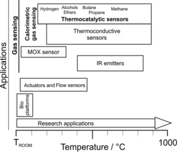
Chapter 2 describes the MEMS microhotplate constraints. Mechanical design, structural materials, reliability and lifetime are investigated by the authors. The lifetime becomes crucial with required operation temperature in excess of 500-550 °C. As the most common application at this temperature is the thermocatalytic detection of methane, the authors investigated the deterioration mechanisms of Pt filament and Pt catalyst activated micropellistror structures.
Chapter 3 presents the general working principal of Scanning Microwave Impedance Microscopy (sMIM) as well as modeling of the sMIM response from dielectric and semiconductor materials to illustrate some practical applications for investigating electronic materials.
Chapter 4 describes the sodium-doped Germanium bulk single crystals, coarse-grain boules and large coarse-grain plates, first obtained and investigated by the authors as a material for infrared optics and detector technique.
Chapter 5 describes the approach to bring together different experimental data regarding metal/semiconductor (M/S) interface on III-V compounds in order to understand the metallurgical characteristics of ohmic contact materials and Schottky barriers.
Representative examples are related to semiconductor materials as n-GaAs, GaAs (SI), n-GaSb, p-GaSb studied in comparative ohmic contact systems in order to identify metallization schemes similarities. The key element for example in GaAs and GaSb devices technology consists in the obtaining of high quality ohmic and Schottky contacts because the surface of these compounds are covered with a native oxide layer. In this view, there are presented some competitive surface preparation procedure e.g. controlled chemical etching, controlled cleavage or Ar+ ion sputtering dedicated to device manufacturing. The morphological and electrical quality of metal thin films deposited on III-V semiconductors have been investigated in different characterization techniques besides others X-ray photoelectron spectroscopy (XPS), Atomic force microscopy (AFM)
or Rutherford back-scattering spectroscopy (RBS). The experimental effort regarding the study of deposited thin metal films on III-V semiconductor compounds is of interest in controlling surface material preparation and processing for developing a competitive technology in dedicated device applications.
Chapter 6 presents authors’ experience in production and characterization of planar optical waveguide layers obtained via proton exchange in lithium niobate. A methodology for characterization of such layers is demonstrated on particular samples which were prepared at different technological regimes aiming to obtain a variety of phases with different quotas composing the proton-exchanged layer.
Chapter 7 discusses the metal oxide nanomaterials obtained by sol-gel and microwave assisted sol-gel methods.
Chapter 8 is devoted to the new heterostructures for higher power microwave DA-pHEMTs. It shows that donor-acceptor doping used to create localization barriers makes possible to increase the effective QW depth significantly, up to 800-900 meV, describes the results of the study of structural, optical and electrical characteristics of DA- pHEMT heterostructures, discusses the scattering mechanisms limiting the 2DEG mobility in such heterostructures and demonstrates the parameters of microwave DA-pHEMTs.
Chapter 9 presents electrothermal simulations of power high-electron mobility transistors (HEMTs) by several simulation methods: 2/3-D device FEM simulation, mixed-mode setup and LEM simulation. Their features and limitations are analyzed. More accurate electrothermal model of the HEMT is proposed and implemented to simulations.
Chapter 10 describes the reading of sensitive data from cache memories and the efficient hardware level countermeasures that can be considered to improve the security.
Chapter 11 reports the cost and power efficient double data rate fourth-generation transmitter with 3-tap equalize with 20 nm process node.
Chapter 12 discusses challenges and opportunities for SiC MOSFETs processing.
Chapter 13 presents a short review on metal oxide semiconductor (MOS) gas sensors and the parameters affecting their performance.
I shall gratefully receive any notices, comments and suggestions from readers to make the next volume of 'Advances in Microelectronics: Reviews' interesting and useful.
Dr. Sergey Y. Yurish Editor
IFSA Publishing Barcelona, Spain
Inertial Sensors
Chapter 1
Design of Au-based Micro-components
with High Structure Stability for Applications in MEMS Inertial Sensors
Tso-Fu Mark Chang, Chun-Yi Chen, Yota Ishizuka, Minami Teranishi, Takuma Suzuki, Daisuke Yamane, Toshifumi Konishi, Katsuyuki Machida, Kazuya Masu and Masato Sone
11.1. Introduction
MEMS (micro-electro-mechanical systems) is the technology of micro-scale devices.
Examples are sensors, actuators, and mechanical components with simple designs such as micro-cantilevers integrated on the same chip [1]. MEMS is widely used in electronics product, such as an inertial sensor in automobile airbag devices and household game machines. Much attention has been paid to MEMS inertial sensors with wide sensing range and high resolution [2]. Recently, integration of complementary metal-oxide- semiconductor-micro-electro-mechanical system and MEMS (CMOS-MEMS) technology has been developed to design MEMS inertial sensors with improved performance [3, 4]. In order to realize the MEMS structure, a post-CMOS process that will not affect the CMOS properties is required. Electroplating is a promising post-CMOS process to fabricate MEMS devices [5] because of the simple process conditions and low temperature process, which is important since heat is one of the major factors affecting properties of the CMOS. In addition, properties of the electroplated materials can be precisely controlled by the electrochemical parameters. Therefore, electroplating can be employed in fabrication of the MEMS inertial sensors.
In previous studies, we have developed a design of MEMS inertial sensor with enhanced sensitivity [6-8]. A schematic diagram of the Au-based MEMS inertial sensor is shown in Fig. 1.1. The high sensitivity is mostly contributed by using Au-based materials as the proof mass, because density of Au is almost ten times higher than silicon, which is the
Tso-Fu Mark Chang
Institute of Innovative Research, Tokyo Institute of Technology, Yokohama, 226-8503, Japan
common material in MEMS devices. Density of Au is 19.3 g/cm3, and Si is 2.33 g/cm3 [9]. The high density is beneficial in reducing Brownian noise, and reducing Brownian noise can directly contribute to sensitivity enhancement and allow further miniaturization of MEMS inertial sensors. Au materials are known to have special characteristics such as high chemical stability, corrosion resistance, electrical conductivity and density. These are all advantageous when applied as electronic components and fabrication processes of MEMS devices [10-12].
Fig. 1.1. Schematic design of an Au-based MEMS inertial sensor.
On the other hand, Young’s modulus and yield strength [13, 14] of Au are relatively low when compared with other materials commonly used in MEMS, and the structure stability becomes a concern in the applications. Based on Euler–Bernoulli beam theory [15], the structure stability is highly related to Young's modulus of the material used to fabricate the movable structures. Young's modulus of Au is 78.5 GPa [16], which is considered to be low when compared to the other commonly used materials in electronic devices, such as Cu (128 GPa) and Si (165 GPa) [17]. Therefore, the structure stability is expected to be enhanced when using a multi-layered design composed of a (or multiple) layer of materials having Young's modulus higher than that of Au. Young's modulus of Ti is 120.2 GPa [16]. Hence, Ti/Au multi-layered design was proposed to solve the concern on structure stability of Au-based materials [6-8]. In addition, Ti can be used as the barrier layer and deposition of a Ti layer is a handy process in fabrication of electronic components.
For practical applications of the Ti/Au multi-layered design in MEMS devices, structure stability of micro-components utilizing the Ti/Au multi-layered design are evaluated. At first, mechanical properties of micro-scaled pillars utilizing the Ti/Au multi-layered design are characterized by micro-compression tests and finite element method (FEM) simulations. Then structure stability of the Ti/Au multi-layered micro-cantilever with different aspect ratio and different constraint condition at the fixed end is evaluated.
Electronic devices can experience extreme environment such as the low temperature in airplane’s baggage compartment or high temperature inside a car in a hot sunny day.
Therefore, temperature structure stability of the Ti/Au micro-cantilevers is evaluated.
Inertial Sensors
1.2. Micro-mechanical Properties of Ti/Au Multi-layered Pillar
Structure stability of a material is highly related to its mechanical properties. In this section, mechanical properties of micro-pillars composed of the Ti/Au multi-layered design are evaluated by micro-compression test and FEM simulation to clarify the effect on enhancement of the mechanical strength. Dimensions of the pillars are in micro-scale to include the sample size effect on the mechanical properties [13].
Ti/Au multi-layered structures are prepared on a silicon substrate by series of Ti sputtering, Au sputtering as the seed layer, and Au electroplating [6]. Three types of the Ti/Au multi-layered structure are evaluated. One is composed of four Ti/Au layers (ML4).
Designed values of thickness of all the Ti layers (tTi) are 0.1 μm, and designed thicknesses of the Au layer (tAu) from the 1st to the 4th layer are 0.5, 3, 3, and 12 μm. The other structure is made up of five Ti/Au layers (ML5), which is having an additional Ti/Au layer on the ML4 structure and tAu of the 5th Au layer is 10 μm. The last one is another Ti/Au layer with the tAu at 15 μm on the ML5 structure (ML6). An example of the ML5 structure is shown in Fig. 1.2.
Fig. 1.2. Example of a structure composed of five Ti/Au layers (ML5).
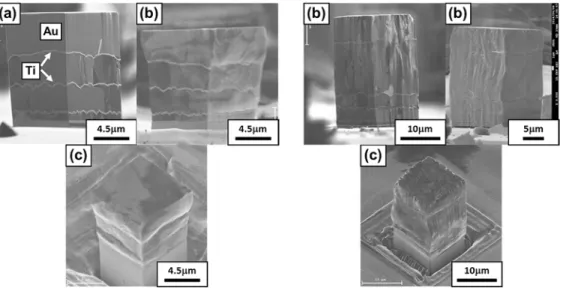
For the micro-compression test, micro-pillars with a square cross-section are fabricated from the Ti/Au multi-layered structure by focus ion beam (FIB) milling as shown in Fig. 1.3. A flat top surface is needed for the compression test, hence some portion of the top layer is milled away by the FIB. Dimensions of the ML4, ML5, and ML6 pillars fabricated are 11×11×12.5 μm3, 15.5×15.5×27 μm3, and 19×19×42 μm3, respectively.
Images of the three as-fabricated micro-pillars are shown in Figs. 1.4(a), 1.5(a) and 1.6(a).
The micro-compression tests are conducted with a testing machine specially designed for micro-specimens. The compression is conducted at a constant displacement rate of 0.1 μm/s using a piezo-electric actuator. Details of the micro-pillar fabrication procedures and the micro-compression test are reported in a previous work [18].
After the compression test, the top Au layer experiences the highest degree of deformation when compared with other Au layers. Especially for the ML4 specimen shown in Figs. 1.4(b) and (c), the top Au layer deforms into a barrel-shape, which is a typical deformation behavior of specimens composed of polycrystals. The difference in degree of the deformation between each Au layer in a pillar is suggested to be caused by the Ti layers, although the tTi is only 0.1 μm. The strain should distribute evenly along the loading direction for specimens compose of the same material. In this case, strengths of Ti are much higher than those of Au. Hence, penetration of the strain from top surface to bottom of the pillar is restrained for some degree at each Au and Ti interfaces, and results the gradual decrease in degree of the deformation from the top Au layer to the bottom Au layer.
Fig. 1.3. FIB fabrication of the Ti/Au Multi-Layered Pillar.
Fig. 1.4. Side view of the as-fabricated four Ti/Au layered micro-pillar (ML4) (a) before and (b) after the compression test, and (c) tilted view of the deformed micro-pillar.
Fig. 1.5. Side view of the as-fabricated five Ti/Au layered micro-pillar (ML5) (a) before and (b) after the compression test, and (c) tilted view of the deformed micro-pillar.
Inertial Sensors
Fig. 1.6. Side view of the as-fabricated six Ti/Au layered micro-pillar (ML6) (a) before and (b) after the compression test, and (c) tilted view of the deformed micro-pillar.
After the compression test, engineering stress (σE) and engineering strain (εE) are calculated using the following equations.
E 0
P
A , (1.1)
E 0
H
H , (1.2)
where P is the applied force, A0 is the cross-sectional area before the compression test, ∆H is the displacement of the indenter, and H0 is the height of the pillar before the compression test. In mechanical testing of micro-specimens, the yield point between the elastic and plastic regions is usually not clear, and the yield stress is determined by the cross-point of the stress-strain (SS) curve and 0.2 % offset line of the elastic deformation region [19]. SS curves generated from micro-compression tests of the three Ti/Au multi- layered pillars are shown in Fig. 1.7. The 0.2 % yield stress are 134.2, 196.4, and 196.6 MPa for the ML4, ML5, and ML6 pillar, respectively. The 0.2 % yield stress is increased as number of the Ti/Au layer increases. The Ti layers would restrain the deformation, hence movement of dislocations across each Ti layer is limited to cause the increase in the 0.2 % yield stress.
FEM simulations are conducted to evaluate the strengthening effect caused by the Ti/Au multi-layered design. The simulations are conducted using COMSOL Multiphysics ver. 5.2a. Simulations of three pillars each having the same dimensions as the ML4, ML5, and ML6 but composed of entirely pure Au are studied as comparisons. Three more pillars having the same dimensions and structure as the ML4, ML5, and ML6 evaluated in the micro-compression test are evaluated.
Fig. 1.7. Engineering stress-strain curves of the ML4, ML5, and ML6 micro-pillars.
After the compression, the pillars composed of entirely gold all show the typical barrel-shape deformation as shown in Fig. 1.8. Cross-sectional areas of the two retrained surface, top surface where it has contact with the indenter and bottom surface where it has contact with the substrate, remain almost constant after the compression. The cross-sectional area gradually increases toward middle part of the pillar. On the other hand, in Fig. 1.9, the three Ti/Au multi-layered pillars show similar deformation behaviors as those observed from the micro-compression test, especially for the ML4 structure. In Fig. 1.9(a), each Au layer exhibits its own barrel-shape deformation, and the top Au layer has the highest degree of deformation, which the cross-sectional area is the largest among the four Au layers in the ML4 structure.
Fig. 1.8. FEM simulation results of pure Au micro-pillars having the same dimensions as the (a) ML4, (b) ML5, and (c) ML6 micro-pillars.
Fig. 1.9. FEM simulation results of the (a) ML4, (b) ML5, and (c) ML6 micro-pillars.
Inertial Sensors
The SS curves generated by the FEM simulations are shown in Fig. 1.10. For the three entirely Au pillars, the simulation results are all the same and labeled as Au monothetic in Fig. 1.10. For the entirely Au, the 0.2 % yield stress is 262.1 MPa. The value is higher than that of the bulk Au, which is results of the sample size effect [13]. 0.2 % yield stresses of the ML4, ML5, and ML6 pillars are 264.7 MPa, 265.2 MPa, and 265.6 MPa, respectively. Again, the 0.2 % yield stress increases with an increase in number of the Ti/Au layer. The trend corresponds well with the trend observes from the micro-compression test.
Fig. 1.10. Engineering stress-strain curves of the ML4, ML5, and ML6 micro-pillars generated by the FEM simulations.
The Ti/Au multi-layered design is confirmed to have a positive effect on strengthening of structures in micro-scale from micro-compression tests and FEM simulations. Mechanical strengths of Ti are much larger than those of Au, but ratio of the Ti layers in the pillar is very small. Hence, the difficulty for dislocations to move across the Ti/Au interface is suggested to play an important role in the strengthening.
1.3. Structure Stability of Ti/Au Single Layered Cantilever
The Ti/Au multi-layered design has been applied in MEMS inertial sensors [6-8], and the multi-layered design is expected to allow further size reduction and improvement in the sensitivity of MEMS devices. In this section, structure stability of Ti/Au single layered micro-cantilevers is investigated by observing tip deflection (∆htip) of the micro-cantilever using a 3D optical microscope (OM) and FEM simulations.
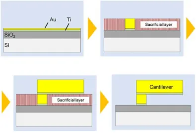
Fig. 1.11 shows fabrication process of the Ti/Au single layered micro-cantilevers. The Ti layer is formed by evaporation to be used as the barrier layer on SiO2 deposited silicon wafer. Then a thin layer of Au is also evaporated to be used as the seed layer in Au electroplating. After deposition of the seed layer, series of lithography and electroplating processes are conducted to fabricate the micro-cantilevers. More details of the lithography and electroplating processes could be found in a previous study [6]. The micro-cantilevers
are annealed at 310 °C during the fabrication process, which is the highest temperature used in the MEMS fabrication process.
Fig. 1.11. Fabrication process of the Ti/Au single layered micro-cantilever.
Fig. 1.12 shows a schematic view of the Ti/Au single layered micro-cantilever composed of an electrodeposited Au upper layer and an evaporated Ti bottom layer on a SiO2
deposited silicon wafer. Designed values of the dimensions are list in Table 1.1.
Fig. 1.12. Schematic view of the Ti/Au single layered cantilever.
Table 1.1. Design parameters of the Ti/Au single layered micro-cantilevers.
l [μm] w [μm] tAu [μm] tTi [μm]
100 ~ 500 10 3, 10, 12 0.1
Top view of the as-fabricated micro-cantilevers is observed by an OM shown in Fig. 1.13, and distance between each micro-cantilever is 100 μm. From the top view, there is clearly
Inertial Sensors
no deformation in directions parallel to the substrate surface. The result is expected since deformation in directions parallel to the substrate surface is mostly caused by inadequate fabrication process or poor handling of the samples. More details of micro-cantilevers can be observed from a tilted view image by a scanning electron microscope (SEM), and the image is shown in Fig. 1.14. The fixed end is composed of the Ti/Au multi-layered design.
On the other hand, there is no contact between the micro-cantilever and top surface of the substrate from the SEM observation.
Fig. 1.13. Optical photomicrograph of the as-fabricated Ti/Au single layered micro-cantilevers.
Fig. 1.14. SEM image of the as-fabricated Ti/Au single layered micro-cantilevers magnified at fixed end.
Height profiles of the micro-cantilevers with the tAu = 3 (Fig. 1.15), 10 (Fig. 1.16), and 12 μm (Fig. 1.17) are measured by the 3D OM. In general, all the micro-cantilevers showed a downward deflection because of self-weight of the micro-cantilevers. This is why the Ti layer is used as the bottom layer to improve the structure stability. In addition, degree of the downward ∆htip increases as the length (l) increases, which indicates a weakened structure stability as the l increases.
Regarding effect of the tAu, the structure stability is high when the tAu is thick. For the micro-cantilever with the tAu = 3 μm and the l = 500 μm, entire body of the cantilever bends downward, and the tip becomes very close to surface of the silicon wafer as shown in Fig. 1.15. Even for the micro-cantilever with a shorter l at 100 μm, the cantilever is not straight. When the tAu is increased to 10 and 12 μm, the ∆htip gradually decrease. A summary of ∆htip’s of the micro-cantilevers with a fixed w, various tAu and the l varied from 100 to 500 μm is shown in Fig. 1.18.
Fig. 1.15. Height profiles of the Ti/Au single layered micro-cantilevers with w = 10 µm, tAu = 3 µm, and l varied from 100 to 500 µm.
Fig. 1.16. Height profiles of the Ti/Au single layered micro-cantilevers with w = 10 µm,
tAu = 10 µm, and l varied from 100 to 500 µm.
Fig. 1.17. Height profiles of the Ti/Au single layered micro-cantilevers with w = 10 µm, tAu = 12 µm, and l varied from 100 to 500 µm.
Inertial Sensors
Fig. 1.18. Tip deflections of the Ti/Au single layered micro-cantilevers with w = 10 µm, tAu = 3, 10, and 12 µm, and l varied from 100 to 500 µm.
Effects of the width (w) on the ∆htip, or the structure stability, are summarized in Fig. 1.19.
Again, ∆htip of the micro-cantilever decreases as the l increases, but there is no obvious difference between micro-cantilevers with different w. That is, there is no width dependency in the structure stability.
Fig. 1.19. Tip deflections of the Ti/Au single layered micro-cantilevers with w = 5, 10, and 15 µm, tAu = 10 µm, and l varied from 100 to 500 µm.
Effects of the Ti/Au f structure on the structure stability are evaluated by FEM (Finite Element Method) simulations [20]. Dimensions and structures of the micro-cantilevers evaluated are the same as those studied in the OM observation, shown in Fig. 1.12 and Table 1.1. Results obtained from the OM observation and the FEM simulations are compared with each other. The FEM simulations are conducted using COMSOL Multiphysics to model deformation behaviors of the Ti/Au single layered micro-cantilevers. The micro-cantilever is modeled on a beam part by using original material constants provided by COMSOL [21]. Fixed end constraint conditions are used to monitor the ∆htip, and symmetry condition is applied along the l of the micro-cantilever to reduce the computation time. The equations of linear elastic material are selected in the category of solid mechanics. The properties of linear elastic materials such as Young's
modulus, thermal expansion coefficient, Poisson's ratio and density are applied in the simulation. Young’s modulus of Ti and Au are 115.7 and 78.5 GPa, respectively, thermal expansion coefficient of Ti and Au are 8.6×10⁻⁶ and 14.2×10⁻⁶ K-1, respectively [16]. The effect of an increase in the temperature from 20 to 310 °C on deformation behaviors of the micro-cantilevers is simulated. Based on the above conditions, the FEM simulations are performed.
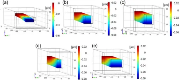
Fig. 1.20 shows FEM simulation results of the micro-cantilever with the l varied from 100 to 500 µm, the w of 10 µm and the tAu of 10 µm. For all of the micro-cantilevers, downward ∆htip’s are observed. Degree of the deflection is increased as l of the micro-cantilevers increases.
Fig. 1.20. FEM simulation results of the Ti/Au single layered micro-cantilever with w = 10 µm, tAu = 10 µm and l at (a) 100 µm, (b) 200 µm, (c) 300 µm, (d) 400 µm and (e) 500 µm.
FEM simulation results of the micro-cantilevers with different tAu and w are shown in Fig. 1.21. Downward ∆htip’s are observed in all of the micro-cantilevers. Also, an increase in tAu leads to a smaller ∆htip and better structure stability as shown in Figs. 1.21 (a) to (c).
Results of micro-cantilevers with different w are shown in Figs. 1.21 (b), (d), and (e), which the w is varied from 5 to 15 µm. For the micro-cantilevers with different w, downward ∆htip’s are observed. No obvious change in the ∆htip is observed when the w changes. As shown in the FEM simulation results, the ∆htip’s are considered to be mainly
Inertial Sensors
caused by the difference in thermal expansion coefficient between Ti and Au, because the MEMS fabrication process involves heat treatment at 310 °C. Thermal expansion coefficient of Au is larger than that of Ti, and Au is the top layer, hence degree of the volume expansion of the top layer will be larger than that of the bottom layer to cause a downward deflection.
Fig. 1.21. FEM simulation results of 100 µm long micro-cantilevers with (a) w = 10 µm and tAu = 3 µm, (b) w = 10 µm and tAu = 10 µm, and (c) w = 10 µm and tAu = 12 µm,
(d) w = 5 µm and tAu = 10 µm and (e) w = 15 µm and tAu = 10 µm.
Fig. 1.22 shows ∆htip results obtained from the OM observation and the FEM simulation for the micro-cantilevers with the l varied from 100 to 500 µm, the tAu fixed at 10 µm, and the w fixed at 10 µm. Both the OM observation and the FEM simulation results show an increase in degree of the ∆htip, and poorer structure stability is observed with an increase in l of the micro-cantilever. The downward deflections are larger for the results by FEM simulation when compared with results from the OM experiments. Table 1.1 shows a summary of the ∆htip obtained by the OM observation and the FEM simulation for the micro-cantilevers with the l of 100 µm, the w of 10 µm, and the tAu’s of 3 µm, 10 µm, and 12 µm. Good agreements are obtained between the OM observation and the FEM simulation results, which the degree of ∆htip lowers as the tAu increases. The differences between the OM observation and the FEM simulation are very small, and the differences might be caused by other factors involved in deformation of the micro-cantilevers, which are not considered in the FEM simulation. For example, metallic Ti oxidizes easily and thin layer of titanium oxides would form on surface of the bottom Ti layer during the fabrication process, especially when annealing treatment is involved. Young's modulus of TiO2 is 270 GPa [5], which is much higher than the value of Au and Ti. Also, the high annealing temperature can contribute to formation of intermetallic at the Ti/Au interface.
Therefore, information of the TiO2 layer, intermetallic layer, and heat treatment conditions should be included in the FEM simulation to provide more precise results.
Fig. 1.22. FEM simulation and OM observation results of tip deflections of Ti/Au single layered micro-cantilevers with w = 10 µm, tAu = 10 µm, and l varied from 100 to 500 µm.
Effects of the length, thickness and width on the structure stability can be explained by the Euler–Bernoulli beam theory for cantilever beams with uniformly distributed load [15]. The equations of Euler–Bernoulli beam theory for cantilever beams with uniformly distributed load are listed as follows:
Shear force at the fixed end (Q):
𝑄 𝑞𝑙 (1.3)
Deflection at the tip (∆htip):
4
tip 8
h ql
EI (1.4)
Second moment of area (I):
Au Ti
312
t t w
I
, (1.5)
where q is the distributed load, in other words a force per unit length, l is the length of the cantilever, E is the Young's modulus, tAu is the thickness of the Au layer, tTi is the thickness of the Ti layer, and w is the width of the cantilever. According to the theory, equation (1.4), degree of bending or deflection at tip of the cantilever (∆htip) is increased with an increase in the l. An increase in the tAu would lead to an increase in the I according to equation (1.5), which then cause a decrease in the ∆htip according to equation (1.5). Based on these equations, results shown in Fig. 1.22 and Table 1.2 correspond well to the Euler-Bernoulli beam theory. On the other hand, as shown in Fig. 1.19, the ∆htip’s did not vary much for the micro-cantilevers when the w varies. This might be because the w has a relatively low influence to the ∆htip when compared with the other parameters, as shown in equation (1.5).
Inertial Sensors
Table 1.2. Comparison of the tip deflection of the micro-cantilevers with the length of 100 µm, the width of 10 µm, and the Au thickness of 3 μm, 10 μm and 12 μm obtained by the OM
and FEM simulation.
tAu
[μm] Tip deflection, ∆htip [μm]
OM observation FEM simulation
3 -0.88 -0.63
10 -0.06 -0.08
12 -0.07 -0.07
In this section, deformation behaviors of Ti/Au single layered micro-cantilevers with different dimensions are evaluated by OM observation and FEM simulations. The ∆htip
observed in the simulation is suggested to be mainly caused by the difference in thermal expansion coefficient between Ti and Au. Results obtained from the OM observation and the FEM simulation all show downward ∆htip for the micro-cantilevers, and the degrees of ∆htip are similar between both methods. Effects of the l, tAu, and w on the ∆htip are in good agreement between the OM observation, the FEM simulation, and Euler–Bernoulli beam theory, which the structure stability becomes worse with an increase in the l and when the tAu is too thin.
1.4. Effect of the Constrained Fixed End on the Structure Stability of Ti/Au Single Layered Cantilever
In practical applications of the Ti/Au multi-layered design in MEMS devices, constraint conditions at fixed end of the micro-cantilever structure could vary. Top surface at the fixed end can be either free or exposing to air, and the bottom surface can be constrained to a structure. Also, both the top and bottom surface can be sandwiched between two other structures. Constraint conditions at the fixed end will affect deformation behavior and structure stability of the micro-cantilever, which would influence practical implantation of the Ti/Au multi-layered structure in MEMS devices. Therefore, in this section, effects of constraint conditions at the fixed end, such as constraining both the top and the bottom surfaces or the bottom surface only, on structure stability of micro-cantilevers comprised of the Ti/Au single layered structure will be reported. The evaluations are carried out by measuring the tip deflection (∆htip) using results obtained from a 3D optical microscope (OM) and finite element method (FEM) simulations.
Fig. 1.23 shows SEM images of the Ti/Au single layered micro-cantilevers fabricated by a series of lithography and electroplating processes. More details of the fabrication processes are provided in a previous study [6]. A schematic diagram of the Ti/Au micro-cantilever is shown in Fig. 1.24. Two types of the micro-cantilever are studied.
Type one is with constraint on bottom surface of the fixed end only. Type two is with constraints on both top and bottom surfaces of the fixed end. Micro-cantilevers with different dimensions are prepared. Width (w) of the micro-cantilevers is fixed at 15 μm.
Thickness of the Au layer (tAu) is 15 μm. Thickness of the Ti layer (tTi) is 0.1 μm. Various length (l) of the micro-cantilevers are used, which are 50, 100 and 200 μm.
Fig. 1.23. SEM image of the (a) Ti/Au micro-cantilevers array with the length varied from 50 µm to 200 µm, width of 15 µm and Au thickness of 15 µm, the (b) type one and the (c) type two Ti/Au micro-cantilevers with a length of 50 µm, width of 15 µm and Au thickness of 15 µm.
Fig. 1.24. Schematic diagrams of the (a) type one and the (b) type two Ti/Au micro-cantilevers.
Structure stability of the Ti/Au micro-cantilevers are evaluated by observing height profile of the micro-cantilevers using an OM equipped with a 3D measurement function. Height of top surface of the micro-cantilever (hx) at a position x away from the fixed end is determined along long-side of the micro-cantilever in a step size (d) of 0.1 μm by the OM.
The structure stability is quantified by calculating the height difference along the micro- cantilever body (Δhx), which is the difference between the hx and the height at the fixed end (h0). The equation is shown in the following:
0
x x
h h h
. (1.6)
For the type two micro-cantilevers, because of the constraint on top surface of the fixed end, height of the top surface of the micro-cantilever body at a location very close to the fixed end is used as the h0. The deflection at the tip (Δhtip) and average deformation of the entire micro-cantilever (Δhave,l) are also calculated. The equation for Δhave,l is shown in the following:
1 ave,
ld x x l
h d
h l
, (1.7)Inertial Sensors
where l is the total length of the micro-cantilever. d is the step size of the measurement, which is 0.1 μm in this case. Fig. 1.25 shows height difference profile of the two types of the Ti/Au micro-cantilevers with the l of 50, 100, and 200 μm observed by the OM. The red horizontal line represents the height at the fixed end, which is used as the baseline to determine deformation of the micro-cantilevers. In Fig. 1.25 (a), height of the type one (only bottom constrained) micro-cantilever at different location along the long-side deviates significantly from the baseline. It gradually bends downward from the fixed end to the tip. Downward deflections of 1.55 to 2.26 µm are observed at the tip as the l increases from 50 to 200 µm as shown in Table 1.3. The Δhave,l increases from 0.883 to 1.560 µm as the l increases from 50 to 200 µm. The results indicate structure stability of the Ti/Au micro-cantilever is lowered with an increase in the l. This behavior occurs because of the increase in the beam’s own weight as the l increases, which follows the Euler-Bernoulli beam theory well. Nerveless, the deformation is still insignificant when compared with length of the micro-cantilever, which demonstrates the Ti/Au multi-layered design’s positive contribution to the structure stability.
Table 1.3. Structure stability determined from the OM results.
Fig. 1.25. Height difference, Δh, profile of the (a) type one and the (b) type two micro-cantilever with a length of 50, 100, 200 µm measured by the OM; the red line represent Δh = 0
along the entire l.