Influence of 20 MeV electron irradiation on the optical properties and phase composition of SiOx thin films
Temenuga Hristova-Vasileva, Peter Petrik, Diana Nesheva, Zsolt Fogarassy, János Lábár, Sonia Kaschieva, Sergei N. Dmitriev, and Krassimira Antonova
Citation: Journal of Applied Physics 123, 195303 (2018); doi: 10.1063/1.5022651 View online: https://doi.org/10.1063/1.5022651
View Table of Contents: http://aip.scitation.org/toc/jap/123/19 Published by the American Institute of Physics
Articles you may be interested in
Kinetically controlled indium surface coverage effects on PAMBE-growth of InN/GaN(0001) quantum well structures
Journal of Applied Physics 123, 195302 (2018); 10.1063/1.5025671
Enhancement of emission of InGaN/GaN multiple-quantum-well nanorods by coupling to Au-nanoparticle plasmons
Journal of Applied Physics 123, 193101 (2018); 10.1063/1.5022454
New photoelectrical properties of InN: Interband spectra and fast kinetics of positive and negative photoconductivity of InN
Journal of Applied Physics 123, 195701 (2018); 10.1063/1.5022844
Structural, optical, and electrical properties of unintentionally doped NiO layers grown on MgO by plasma- assisted molecular beam epitaxy
Journal of Applied Physics 123, 195301 (2018); 10.1063/1.5026738
Tutorial: Determination of thermal boundary resistance by molecular dynamics simulations Journal of Applied Physics 123, 191101 (2018); 10.1063/1.5027519
Effects of etchants in the transfer of chemical vapor deposited graphene Journal of Applied Physics 123, 195103 (2018); 10.1063/1.5009253
Influence of 20 MeV electron irradiation on the optical properties and phase composition of SiO
xthin films
TemenugaHristova-Vasileva,1PeterPetrik,2DianaNesheva,1ZsoltFogarassy,2 JanosLab ar,2SoniaKaschieva,1Sergei N.Dmitriev,3and KrassimiraAntonova1
1Institute of Solid State Physics, Bulgarian Academy of Sciences, 72 Tzarigradsko Chaussee Blvd., 1784 Sofia, Bulgaria
2Centre for Energy Research, Hungarian Academy of Sciences, H-l12l Budapest, Konkoly Thege Miklos ut 29-33, Hungary
3Joint Institute for Nuclear Research, Flerov Laboratory of Nuclear Reactions, Dubna, Moscow Region 141980, Russia
(Received 17 January 2018; accepted 29 April 2018; published online 21 May 2018)
Homogeneous films from SiO1.3 (250 nm thick) were deposited on crystalline Si substrates by thermal evaporation of silicon monoxide. A part of the films was further annealed at 700C to grow amorphous Si (a-Si) nanoclusters in an oxide matrix, thus producing composite a-Si-SiO1.8 films. Homogeneous as well as composite films were irradiated by 20-MeV electrons at fluences of 7.21014 and 1.441015 el/cm2. The film thicknesses and optical constants were explored by spectroscopic ellipsometry. The development of the phase composition of the films caused by the electron-beam irradiation was studied by transmission electron microscopy. The ellipsometric and electron microscopy results have shown that the SiOx films are optically homogeneous and the electron irradiation with a fluence of 7.21014el/cm2has led to small changes in the optical con- stants and the formation of very small a-Si nanoclusters. The irradiation of the a-Si-SiOxcomposite films caused a decrease in the effective refractive index and, at the same time, an increase in the refractive index of the oxide matrix. Irradiation induced increase in the optical band gap and decrease in the absorption coefficient of the thermally grown amorphous Si nanoclusters have also been observed. The obtained results are discussed in terms of the formation of small amorphous sil- icon nanoclusters in the homogeneous layers and electron irradiation induced reduction in the nano- cluster size in the composite films. The conclusion for the nanoparticle size reduction is supported by infrared transmittance results.Published by AIP Publishing.https://doi.org/10.1063/1.5022651
I. INTRODUCTION
It is well known that ion or electron irradiation of solids normally causes the formation of atomic defects in a solid state target and spoils its properties.1 Irradiation-induced amorphization, recrystallization, and annealing may change various properties of solid-state materials and devices, which can be followedin situby optical methods.2Therefore, dur- ing the last few decades, there was significant activity to explore such alterations in various types of semiconductor devices, in particular, in metal-oxide-silicon (MOS) struc- tures and microelectronic elements.3On the other hand, ion- izing radiation is also applied for the synthesis of various materials, in particular, nanomaterials.4
Silicon nanoparticles have been studied actively in recent years because they are promising for application in various types of semiconductor devices, such as MOS based nonvola- tile memories5–7and third generation solar cells.8–12We have shown that MOS structures with silicon nanocrystals are also promising for detectors of ionizing radiation.13,14
Most frequently, Si nanoparticles are grown by high temperature thermal annealing of nonstoichiometric silicon oxides, but electron or ion beams irradiation has also been applied as a tool for growing and processing Si nanopar- ticles. Phase separation in Si-enriched silicon oxide films15,16 as well as annealing of Si nanocrystals17have been reported
under irradiation with high-energy (several tens of MeV) ion beams. It has also been shown that high intensity electron beams (current density>1 A/cm2) with electron energies of less than 1 MeV can induce the formation of silicon nanopar- ticles.18–21However, to the best of our knowledge, the infor- mation on the effect of irradiation with electrons having energies higher than 10 MeV on the nanoparticle growth pro- cesses in silicon oxide and the lattice structure of Si nanopar- ticles (crystallization/amorphization, level of disorder) is very limited. Investigations on 20 nm thick SiO2films have shown that the irradiation with 20-MeV electrons induced the formation of Si nanocrystals at fluences of 1016–1017el/
cm2.22,23 In a previous investigation on 20-MeV electron irradiated homogeneous 200 nm thick silicon suboxide films (SiOx,x¼1.3), we have found that the surface roughness of the film decreased, some structural changes in the oxide matrix took place, and a small amount of amorphous silicon phase appeared.24Further investigations by various comple- mentary techniques will allow to get more information about the effect of the 20 MeV-electron irradiation on the phase separation and Si nanocluster formation processes in homo- geneous SiOxfilms and the amount of the pure silicon phase and the size of nanoclusters in composite Si-SiOx films.
Such information could also be helpful for considering the possibility for the development of high-energy electron
0021-8979/2018/123(19)/195303/8/$30.00 123, 195303-1 Published by AIP Publishing.
detection by MOS structures with homogeneous SiOxfilm or a-Si-SiOxcomposite film in the gate dielectric.
In this work, the effect of irradiation with 20-MeV elec- trons of homogeneous SiOx films and a-Si-SiOx composite layers containing amorphous silicon nanoclusters has been investigated by applying spectroscopic ellipsometry (SE) combined with transmission electron microscopy (TEM) and infrared transmission measurements. Thus, information has been obtained about the electron-beam induced changes in the energy dispersion of the refractive index and absorption coefficient, the SiOxfilms composition, and the presence of pure silicon phase and its amount.
II. EXPERIMENTAL DETAILS
Silicon suboxide (SiOx) layers with an initial composi- tion of x¼1.3 and thickness of 250 nm were prepared by thermal evaporation of SiO from a tantalum crucible heated up to 1250C at a vacuum of 1103Pa.25 The films were deposited on p-type (100) crystalline silicon substrates (c-Si), cleaned chemically, and maintained at room tempera- ture. The deposition rate and film thickness were monitored by a calibrated quartz crystal microbalance system. All as- deposited layers were furnace annealed at 250C for 30 min in an Ar atmosphere to ensure film stability at ambient con- ditions. In the Raman scattering spectra of these films, obtained previously,24 only bands corresponding to scatter- ing from the c-Si substrate have been registered and no scat- tering from a second phase has been observed. These layers form the group of homogeneous SiOxfilms studied here.
A second group of composite films was prepared by an additional annealing of some of the homogeneous films at 700C in Ar for 60 min. Such annealing causes phase separa- tion and formation of amorphous Si (a-Si) clusters in an oxide matrix.25In this case, the samples are considered as a- Si-SiOx[x1.8 (Ref.26)] composite films.
A part of the samples from each group was irradiated in vacuum by 20-MeV electrons with two different fluences, F1¼7.21014el/cm2andF2¼1.441015el/cm2. The irra- diation was carried out in Microtron MT-25 in FLNR, Joint Institute for Nuclear Research, Dubna. During the entire
irradiation process, the beam current was about 5 lA, the temperature of the vacuum box was controlled and kept close to room temperature, and the samples’ temperature should not be much higher than that of the vacuum box.
Electron diffraction patterns were measured in nanobeam diffraction (NBD) mode in a JEOL3010 TEM, operated at 300 keV. The patterns were recorded on an Orius 200D cam- era, controlled by Digital Micrograph software. The largest recorded scattering vector was Qmax¼160 nm1, where Q¼4psin(h)/k. TEM measurements were also performed with a Philips CM20 microscope operated at a 200 kV acceler- ating voltage. The cross-sectional TEM samples were pre- pared by Arþion beam milling without sample cooling and using 10 kV accelerating voltage in the beginning and 3 kV accelerating voltage at the end of the thinning process.
Spectroscopic ellipsometry was applied to study optical constants of the samples since it is a sensitive method for the investigation of semiconductor27 and dielectric nanostruc- tures.28 Multiple angle measurements provide a large num- ber of experimental data, which ensure the accuracy in finding the proper structural model to describe the real struc- ture. The SE measurements were carried out on Woollam’s automatic spectroscopic ellipsometer M2000DI working in the reflection mode. Angles of incidence from 50 to 65by 5have been used in the wavelength range of 193–1000 nm.
The most frequently used models for the evaluation of com- plex samples are the Cody-Lorentz model29and those based on the Bruggeman effective medium approximation (B- EMA).30–32 Therefore, the obtained data were further fitted using Woollam’s CompleteEASE program with the Cody- Lorentz oscillator model. To evaluate the compositional data and to specify the influence of the nanoparticles content on the optical properties of the films, the B-EMA model was applied. The modeled structure is shown in Fig. 1(a), inset.
The native SiO2was not removed from the surface of the c- Si substrates, and therefore, it was taken into account in the fitting procedure. The best fits were obtained for a thickness of about 2 nm. The surface roughness of all films was also taken into account. It has been modeled using the standard procedure of an effective medium composition with 50%
void and 50% layer material.
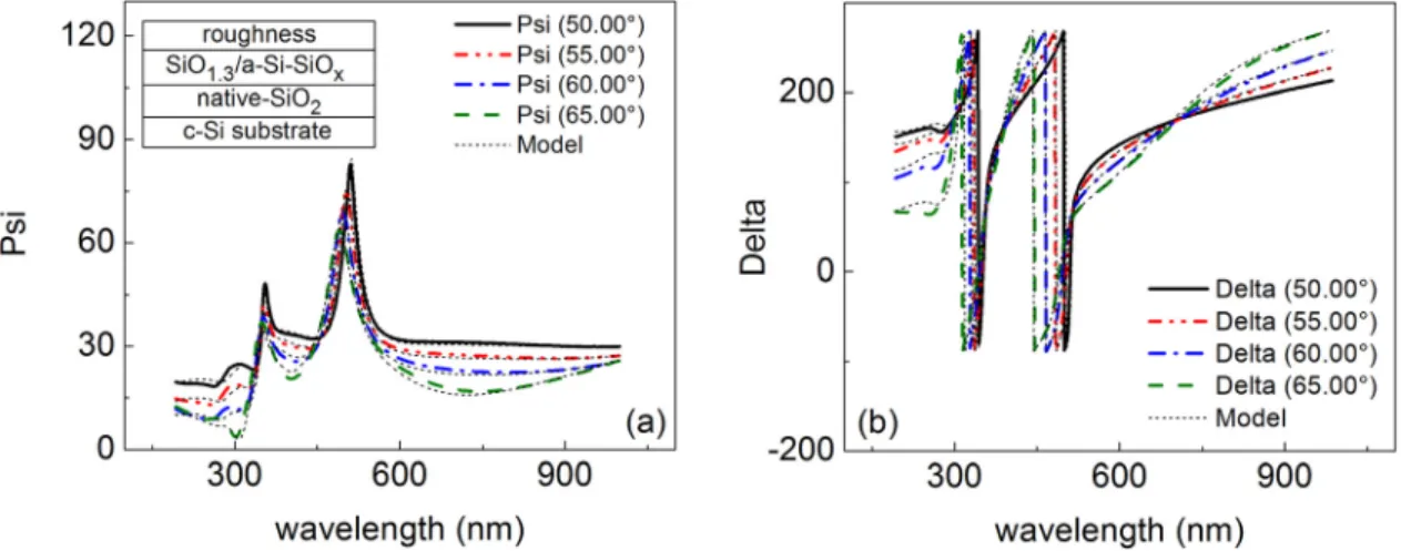
FIG. 1. Experimental spectra and model generated data fits of Psi (a) and Delta (b) of a non-irradiated structure with a homogeneous SiO1.3layer. (a), inset:
Structure assumed and used in the modeling of the SE data.
195303-2 Hristova-Vasilevaet al. J. Appl. Phys.123, 195303 (2018)
Fourier transform infrared (FTIR) transmission mea- surements are frequently used in order to explore the compo- sition and structure of SiOx (x2) films. It is well known33,34 that the main band in the IR spectra of SiO2 observed at 1080 cm1 is due to an asymmetric stretching vibration of the Si–O–Si bridge, which consists of one trans- verse optical (TO) at 1080 cm1and other longitudinal opti- cal (LO) modes in the range of 1200–1300 cm1. There are three modifications of the stretching band that are consistent with a decrease in the oxygen content in SiOxfilms34— the position of the peak is shifted to the low frequencies (“red”
shift) with respect to silica and both the characteristic LO shoulders of the high-frequency side of the band disappear and the full-width at half maximum of the band increases due to changes in the lattice order. In order to get informa- tion about the electron-beam induced changes in the oxygen content of both the homogeneous films and the composition of the matrix of a-Si-SiOxfilms, FTIR transmittance spectra were measured in normal incidence geometry. A Bruker Vertex 70 instrument was operated in the spectral region of 2000–450 cm1with a resolution of 1 cm1.
III. RESULTS AND DISCUSSION A. Homogeneous films
The fit results obtained when applying the Cody- Lorentz oscillator model to the experimental spectra of homogeneous films were presented and analyzed below.
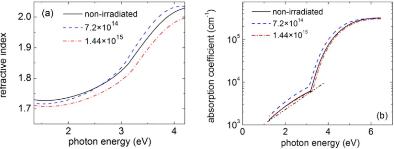
Experimental spectra and model generated data fits of a non-irradiated structure with a homogeneous SiO1.3 layer are shown in Fig.1. The corresponding dispersion curves for the refractive index (n) and absorption coefficient (a) are displayed in Figs.2(a)and 2(b), respectively. As seen from Fig.2(a), the electron irradiation causes a refractive index decrease in the weak absorption range (photon energy<2.5 eV); the larger the irradiation fluence, the stronger the decrease inn.
Previous studies on the effect of 10–25 MeV electron irradiation of bare Si substrates with 2–4 nm native oxide on the surface have shown35 that mostly electrically active defects (complexes of Si vacancy-phosphorus atom or Si
vacancy-boron atom) are created. SE has been used to study the influence of 12 MeV electron beam on the oxide thick- ness of n/p-Si-SiO2structures.36It has been found that, as a result of electron irradiation, oxidation of the n-Si crystalline substrate took place in SiO2 (58 nm)/n-Si system, but this effect was absent for the electron-irradiated SiO2/p-Si system under similar conditions. Hence, one could not expect that irradiation induced changes in the p-Si substrate we used will affect the SE results for the SiOx layer significantly.
It is well known that the refractive index of SiOxfilms depends on their composition; ndecreases with increasing oxygen content xand its value for a given xdepends on the technique applied for the film deposition.37–39Based on this, the observed n-decrease upon electron irradiation can be related to an increase in the oxygen content in the films due to initial phase separation in the layers and formation of Si clusters of a very small size. This assumption is based on the well-known process of SiO2 decomposition to silicon and oxygen under irradiation by an electron beam and oxygen migration described in the literature.40 Electron irradiation- induced migration of atoms has also been observed on the surface of amorphous SiOx nanowire.41 Accordingly, we assume that a small part of the energy of the irradiating MeV-electrons is transferred to the SiOx lattice atoms, and processes of bond breaking, phase separation, and silicon nanocluster formation take place. The structure of the silicon oxide, as the structure of other silicon-based alloys, is built- up from tetrahedral units centered on a silicon atom. The four corners of the tetrahedra in Si-rich SiOxcould be either silicon or oxygen atoms. SiOx films are amorphous and together with the bond length and dihedral angle variation, a high concentration of dangling bonds exists in amorphous films.38The irradiation-created oxygen atoms, which are of a higher mobility in silicon oxide than the Si ones, transport diffusively, and can connect to dangling bonds of some SiOx tetrahedral units, thus increasing the overall oxygen content in the SiOxmatrix. Such increase in the oxygen content of the films is observed25 upon annealing at 700C accompa- nied by the formation of amorphous silicon clusters with average size of around or less than 2 nm.42The very small Si
FIG. 2. Refractive index (a) and absorption coefficient (b) vs. photon energy of non-irradiated and 20-MeV electron beam-irradiated homogeneous SiO1.3
samples. The irradiation fluences are given in el/cm2. The dashed-dotted-dotted straight line in (b) is drawn to demonstrate thataat energies below 3 eV is non-exponential.
clusters cannot be distinguished by the light as a separate phase but the x-increase can be the reason for the film’s refractive index decrease observed.
Electron diffraction measurements were carried out in order to get more information about the assumed Si nano- cluster formation upon 20-MeV electron irradiation. No crystalline silicon nanophase has been observed which meant that if there is a pure Si phase in the irradiated films, it should be amorphous. The cluster formation was revealed by differential pair distribution analysis based on the TEM dif- fraction patterns, rather than a direct observation on HRTEM or EFTEM images. The assumption about the formation of a-Si nanoclusters is in accordance with the results from pre- vious Raman scattering measurements, carried out on the same samples, which indicated the existence of amorphous silicon phase.24
The Pair Distribution Function (PDF) analysis is widely used in x-ray diffraction (XRD), neutron diffraction (ND), and also in electron diffraction.43PDF analysis is the method of structure examination in the case of disordered materials44 Electron diffraction based PDF analysis (ePDF) gives reli- able values for the nearest atomic distances, while numerical values for the coordination numbers are more affected by both inelastic and multiple elastic scattering, which is less of a problem with XRD and ND.45
For non-periodic structures, there exists no simple for- mula that could make simple correlation between the real structure and the diffraction pattern. In contrast to the case of crystalline materials, where the “distances of the lattice planes,” which appear in the Bragg-equation, can directly be seen in the form of rings in the diffraction patterns of poly/
nano-crystalline materials, and the nearest atomic distance values only manifest in the Pair Distribution Function, which is obtained by Fourier-transformation from the measured dif- fraction data. In our work, the values of atomic distances are only used to identify the phases and the qualitative trend in their quantities. The values of atomic distances are obtained from the PDF curves, and they cannot be expected to mani- fest directly in the form of separate rings in the original dif- fraction pattern. However, quantitative coordination data
could be obtained from PDF by Reverse Monte Carlo (RMC) method,46which was not applied in this work.
From the measured intensity distribution, I(Q), the struc- ture factor was deduced as S(Q)¼I(Q)/nf2, where the spher- ically symmetric atomic electron scattering amplitude was calculated with Weickenmeier and Kohl’s method.47 The pair correlation function, G(r), was calculated assuming isot- ropy with
G Rð Þ ¼2 p
ðQmax
1
QS Qð Þ 1
sinQRdQ: (1) The normalized pair distribution, defined by g(R)
¼q(R)/q0, is calculated from G(r).q(R) is the number den- sity of atoms at a distance of R from the center andq0is the average number density. The procedure is coded in the ProcessDiffraction program.48
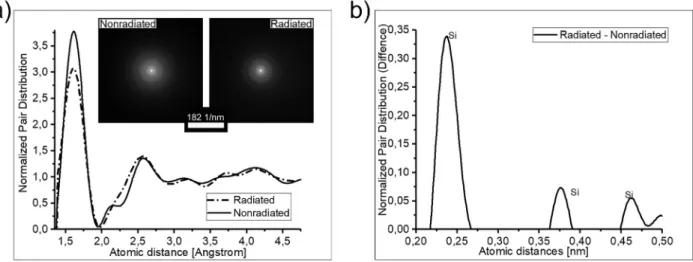
The normalized pair distributions measured for the two samples are compared in Fig. 3(a). The main peak at 1.63 A˚ is a characteristic of SiO2. The Si-O distance in quartz is 1.61 A˚ . The deviation can be attributed to the calibration (expected accuracy is60.6% relative, i.e.,60.01 A˚ absolute deviation at the first peak both in the calibration pattern and the measured pattern). A peak is expected at 2.35 A˚ that cor- responds to the Si-Si distance (which are the same in both crystalline and amorphous forms of silicon, due to the strong bond, see Ref.49). The presence of such a peak can be dis- cerned in the distribution form of the sample irradiated with 7.21014 el/cm2, but it is overlapping with other features, so its identification is not so obvious. On the other hand, when compared to the pair distribution from the non- irradiated sample, this latter might also contain some contri- butions from Si-Si distances, due to non-stoichiometry.
However, the development of the structure caused by the electron-beam irradiation can be seen when the difference between the two distributions is plotted. The difference between the two is shown in Fig.3(b). It contains a negative peak in the 1.6–1.7 A˚ region, indicating that the number of Si-O bonds was reduced in the examined volume of the film.
This observation can be related to electron beam induced
FIG. 3. Normalized pair distributions measured for a non-irradiated sample and a 20-MeV electron irradiated sample (a) and difference between the two distri- butions (b). The irradiation fluence is 7.21014el/cm2. The inset shows the nano-beam diffraction patterns of the nonradiated and the radiated samples.
195303-4 Hristova-Vasilevaet al. J. Appl. Phys.123, 195303 (2018)
oxygen atomic diffusion towards the Si substrate.35 However, the main characteristic feature is 3 positive peaks, which coincide with the first three atomic distances in sili- con. This is a clear proof that the relative amount of Si-Si distances (from elemental Si) has been unambiguously increased in the e-beam irradiated sample as compared to the non-irradiated one. The electron diffraction measurements were carried out from the middle of the layers. Since in this area no silicon nanocrystals have been observed in the cross- section TEM images, the NBD registered nanoclusters should be amorphous.
The spectrum of the absorption coefficientaof homoge- neous SiO1.3 film [Fig. 2(b)] consists of two parts—a part corresponding to the strong (band-to-band) light absorption (at photon energies above 3 eV) and a second part of weak (sub-band) absorption. It is seen from the figure that the weak-absorption part is not exponential. This implies that the weak-absorption is related to electron transitions from various types of defects of a quite high density (a>103cm1 in the 1.0–2.8 eV range) to the conduction band rather than transitions from the valence band to localized states in an exponential conduction band tail or from exponential valence band tail states to the delocalized states of the con- duction band. This can be expected since a variety of defects exist in understoichiometric amorphous SiOxdue to the var- iations in the lattice bond length and the dihedral angle.38 From Fig. 2(b), one can also see that the lower irradiation fluence causes slighta-increase which could be ascribed to an increase in the defects’ density. The coincidences of the a-curve of the sample irradiated with 1.441015 el/cm2 with the curve of non-irradiated one could be explained assuming two competitive processes—creation and
“annealing” of defects. The observed electron irradiation induced significant decrease in the film surface roughness, revealed by atomic force microscopy measurements, has also been related to the electron induced “annealing” effect.24 The atomic diffusion during the film deposition is very restricted since the SiOx films were deposited by thermal evaporation in vacuum (the adatom energy is low, less than 1 eV) at room substrate temperature. Therefore, an increased level of lattice disorder and surface roughness could be
expected which can be reduced due to the above-mentioned electron-beam stimulated atomic diffusion.
The optical band gap,Eg, of the films was determined by the modeling program, as well as using the Tauc relation for amorphous semiconductors and dielectrics a (E-Eg)2 (a—absorption coefficient,E—energy of the absorbed light).
A value of Eg¼3.01 eV has been obtained for the non- irradiated sample which is reasonable for SiO1.3 films.37 Small Eg changes have been obtained (Eg¼2.96 eV and 3.06 eV of the films irradiated with the lower and higher flu- ences, respectively) which can be influenced by the experi- mental errors and therefore we shall not discuss them.
B. Composite films
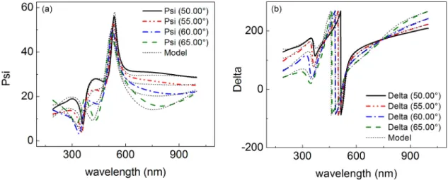
The Bruggeman fitting procedure applied to the SE spec- tra of the composite a-Si-SiOx films (i.e., a-Si nanoclusters embedded in a SiO1.8matrix) allowed us to obtain the optical parameters (effective refractive index/extinction coefficient/
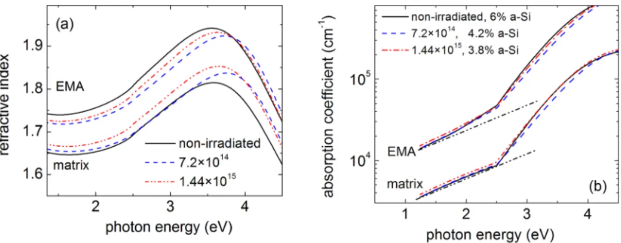
absorption coefficient) of the films considered as an effective medium50,51 and also to get information about the optical parameters of the SiOxmatrix itself. Experimental SE spectra and Bruggeman model generated data fits of a 20-MeV elec- tron beam irradiated sample (a-Si-SiOx film matrix on the crystalline silicon substrate and irradiation fluence of 1.441015el/cm2) are shown in Fig.4. The dispersion curves for the effectivenandaof a non-irradiated and two irradiated a-Si-SiO1.8films are displayed in Figs.5(a)and5(b), respec- tively, as a group of three “EMA” curves. Thenandadisper- sion curves obtained for the SiO1.8 matrix of the composite films are also shown in Fig. 5as a group of “matrix” curves.
As seen from Fig.5(a), the electron-beam irradiation causes a decrease in the effective refractive index nat energies lower than 3 eV. However, the refractive index of the SiOxmatrix displays an increase with the increase in the irradiation flu- ence. As mentioned earlier, the refractive index of homoge- neous SiOxfilms increases with decreasingx. The observed increase in the refractive index of the matrix can be related to an increase in the silicon enrichment in the SiO1.8matrix upon electron irradiation. This could happen, provided a part of the Si atoms in the a-Si nanoclusters moves back to the matrix.
FIG. 4. Experimental and model generated data fits of a structure with a composite a-Si-SiO1.8layer containing amorphous Si nanoparticles. The structure was 20-MeV electron irradiated at a fluence of 1.441015el/cm2.
Should this be the case, one can conclude that the electron beam irradiation causes an overall decrease in the pure sili- con phase, i.e., the nanoparticle size or/and the density of the nanoclusters decreases. The fit results also show that the percentage of the pure silicon phase, which is related to par- ticles that are large enough to be characterized with a dis- tinct dielectric function and, as a result, can be handled by the effective medium theory, decreases from 6% in the non- irradiated sample to 3.8% in the sample irradiated with the higher fluence [Fig. 5(b)]. This result indicates that most likely the electron beam irradiation reduces the volume fraction, and consequently the size of the relatively large nanoclusters (assuming that the number of particles does not change). A similar observation has been reported for ZnO nanoparticles irradiated with 6-MeV electrons over the range of 11015–2.51015el/cm2.52 It has been obtained that the ZnO nanoparticle size was reduced from 46 nm for the non-irradiated samples to 15 nm upon the sample irradiation with the fluence of 2.51015el/cm2.
What could be the reason for the observed decrease in the effective refractive index? It has been shown53,54that the static dielectric constant of ultra-small silicon nanoparticles is smaller than that of the corresponding bulk material.
Hence, the suggested electron-induced size reduction in nanoclusters will lead to a decrease in the dielectric constant (nat photon energies below 2 eV) of the pure Si phase. This effect together with the reduction in the amount of the pure Si phase can be the reason for the observed decrease in the effective refractive index [Fig.5(a)].
It is seen from Fig.5(b)that the shape of the absorption spectra of the composite layers (“EMA”- curves) is a bit dif- ferent from both the shape of the absorption spectra of the corresponding oxide matrices (the same figure, “matrix”
curves) and the shape of the absorption spectra of the homo- geneous SiO1.3 layers [Fig. 2(b)]. Looking at the photon energy range of 2–2.5 eV, it can be noticed thataof the com- posite layer is higher than that of the matrix, which is most likely due to light absorption in the a-Si nanoclusters (the absorption of the composite layers is a combination of the Si nanoclusters and the matrix absorption). In order to distin- guish the a-Si nanocluster absorption, we have calculated it
from the absorption spectra of the matrix and the correspond- ing composite layer using the effective medium theory.
Thus, obtained a-Si nanocluster absorption spectra are plot- ted in Fig.6. It is seen that the optical absorption coefficient of Si nanoclusters in the electron irradiated samples is smaller than that of the nanoclusters in the non-irradiated sample. In addition, the band gap of the Si nanoclusters increases upon electron irradiation.
Previous studies on silicon nanocrystals55 and amor- phous Si nanoclusters56have shown that the NP size reduc- tion causes an Eg increase which is consistent with a strengthening quantum confinement effect in the nanopar- ticles, as well as a decrease in the absorption coefficient with decreasing nanocrystal size.55 Hence, in our case, the observed higher band gap in electron beam irradiated sam- ples can be related to a reduction in the Si cluster size. This assumption is in agreement with the conclusion for radiation induced reduction in the size of the relatively large Si nano- clusters, based on the observed refractive index changes.
FIG. 5. Refractive indexn(a) and absorption coefficienta(b) vs. photon energy of non-irradiated and 20-MeV electron beam irradiated composite a-Si-SiO1.8
films. “EMA” and “matrix” in the figure refer to the results obtained for the effectivenandaof the composite films considered as an effective medium and the SiOxmatrix only, respectively. The EMA spectra ofawere multiplied by 4 and up shifted for clarity. The dash-dot-dot curves in (b) are parallel.
FIG. 6. Absorption spectra of a-Si nanoclusters (alphaa-Si¼alphaEMA- alphamatrix) in non-irradiated and 20-MeV electron beam irradiated a-Si-SiOxcomposite layers. The irradiation fluences and the optical band gaps calculated using the Tauc relation are denoted in the figure.
195303-6 Hristova-Vasilevaet al. J. Appl. Phys.123, 195303 (2018)
Further support for Si nanocluster size reduction is given by the irradiation induced decrease in alphaa-Sithat is well seen in the strong absorption region.
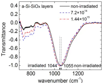
As mentioned above, FTIR transmittance measurements allow to get information about the oxygen content in SiOx (x<2) films (Ref.25and references therein). Our previous FTIR investigations, combined with Rutherford backscatter- ing measurements,26 have shown that the asymmetric transverse-optical (TO) stretching vibration of the Si–O–Si bridge shifts linearly to the lower frequencies when the oxy- gen content decreases. The average dielectric function of the a-Si-SiOxcomposite films has also been calculated by means of the Bruggeman effective medium approximation and a good correspondence between theory and experiment has been found.26
In order to get information about the electron beam induced changes in the composition of the SiOxmatrix of the composite films, we measured FTIR spectra of non- irradiated and electron irradiated films. Normalized IR trans- mittance spectra of non-irradiated and 20-MeV electron beam irradiated a-Si-SiO1.8 films are shown in Fig. 7. As seen from the figure after electron-beam irradiation, the shape of the transmission band is preserved which implies34 that the lattice order in the SiOx matrix is not appreciably changed by the irradiation. However, a considerable “red”
shift of the TO stretching band (of around 10 cm1) is observed. It has been shown that oxygen is preferentially lost during the electron-beam irradiation of a-SiO2 leaving it oxygen deficient18–21,57 which could explain the observed
“red” shift. If oxygen desorption is the reason for the observed red shift it should increase gradually with increas- ing the electron fluence (the irradiation flux was constant and the fluence was increased with increasing irradiation time) but this is not the case. The TO frequency is sensitive to the SiOxdensity, as well. The density decrease causes a red shift of the TO stretching band and one can assume that a decrease in the SiOx matrix density is responsible for the observed red shift. However, investigations on the effect of
the electron beam irradiation on the SiO2density have shown that the electron irradiation causes film densification58–60 and hence a “blue” shift can be expected instead. Our SE data have not shown appreciable difference between the thicknesses of irradiated and non-irradiated films and we assume that the matrix density is not significantly affected by the electron irradiation. The red shift of the TO stretching band can be related to a decrease in the oxygen content in the SiOxmatrix caused by the electron irradiation (fromx1.8 tox1.7, roughly estimated from the relation between the oxygen content xof SiOx layers, determined by Rutherford backscattering, and the position of the TO stretching band in the IR transmission spectra of the layers26). Suchx-decrease could happen if a part of the silicon atoms in the pure silicon phase goes back to the oxide matrix thus causing a nanoclus- ters’ size decrease, which is in agreement with the conclu- sion taken from the SE data.
IV. CONCLUSIONS
The effect of 20-MeV electron beam irradiation at fluen- ces of 7.21014and 1.441015el/cm2on the phase separa- tion and Si nanocluster formation in homogeneous SiO1.3 films and the phase composition of a-Si-SiO1.8 films has been investigated by spectroscopic ellipsometry, transmis- sion electron microscopy and infrared transmission measure- ment. The SE results have shown that an initial phase separation takes place in the homogeneous SiOxfilms upon electron irradiation. The TEM results have supported this and implied that the nanoclusters formed are amorphous.
The light absorption increase in the weak absorption region has been connected with some electron irradiation induced increase in the lattice disorder.
The electron irradiation of the composite a-Si-SiO1.8 films causes: (i) a decrease in their effective refractive index while the refractive index of the SiO1.8matrix increases; (ii) a decrease in the absorption and increase in the optical band gap of the Si nanocluster and (iii) a decrease in the percent- age of the pure silicon phase, related to particles that are large enough to be characterized with a distinct dielectric function. Based on these observations, a conclusion has been made that the electron beam irradiation causes a size reduc- tion in the larger thermally grown silicon nanoclusters. Size reduction in the nanoclusters could also explain the observed softening of the vibrational frequencies upon electron beam irradiation.
Thus, we have shown that the high energy electron irra- diation may have different effects. It can cause initial phase separation and silicon nanocluster formation in homoge- neous SiOx films, but in composite a-Si-SiOx films, it can cause a reduction in the size of the already existing a-Si nanoclusters.
ACKNOWLEDGMENTS
This work has been supported under an exchange grant in the framework of the Bulgarian Academy of Science - Hungarian Academy of Science collaboration, as well as under the OTKA Grant No. K115852. The Bulgarian co-authors thank the European Regional Development Fund, Ministry of
FIG. 7. Normalized infrared transmittance spectra of a non-irradiated and two 20-MeV electron beam irradiated a-Si-SiO1.8composite films contain- ing amorphous silicon nanoparticles. The irradiation fluences are given in the legend in el/cm2.
Economy of Bulgaria, Operational Program “Development of Competitiveness of the Bulgarian economy” 2007–2013, Contract No. BG 161PO003-1.2.04-0027-C0001 for purchasing the spectrophotometer Vertex 70.
1A. V. Krasheninnikov and K. Nordlund, J. Appl. Phys. 107, 071301 (2010).
2P. Petrik, W. Lehnert, C. Schneider, T. Lohner, M. Fried, J. Gyulai, and H.
Ryssel,Thin Solid Films383, 235 (2001).
3N. T. Fourches,Current Topics in Ionizing Radiation Research(InTech, Rijeka, 2012), Chap. 32, p. 741.
4Radiation Synthesis of Materials and Compounds, edited by B. I.
Kharisov, O. V. Kharissova, and U. O. Mendez (CRC Press, Taylor&Francis group LLC, 2013).
5S. Tiwari, F. Rana, H. Hanafi, A. Hartstein, E. Crabbe, and K. Chan,Appl.
Phys. Lett.68, 1377 (1996).
6D. Nesheva, N. Nedev, M. Curiel, I. Bineva, B. Valdez, and E. Manolov, Quantum Dots—A Variety of New Applications(InTech, Rijeka, 2012), p.
183 and references therein.
7T.-C. Chang, F.-Y. Jian, S.-C. Chen, and Y.-T. Tsai,Mater. Today14, 608 (2011).
8G. Conibeer, M. A. Green, R. Corkish, Y.-H. Cho, E.-C. Cho, C.-W. Jiang, T. Fangsuwannarak, E. Pink, Y. Huang, T. Puzzer, T. Trupke, B. Richards, A. Shalav, and K.-L. Lin,Thin Solid Films511–512, 654 (2006).
9T. Nychyporuk and M. Lemiti, in Silicon-Based Third Generation Photovoltaics, Solar Cells—Silicon Wafer-Based Technologies, edited by L. A. Kosyachenko (InTech, Rijeka, 2011).
10S. Yamada, Y. Kurokawa, S. Miyajima, and M. Konagai,Nanoscale Res.
Lett.9, 246 (2014).
11M. Schnabel, C. Weiss, P. L€oper, P. R. Wilshaw, and S. Janz,Phys. Status Solidi A212, 1649 (2015).
12V. Svrcˇek, C. McDonald, M. Lozac’h, T. Tayagaki, T. Koganezawa, T.
Miyadera, D. Mariotti, and K. Matsubara,Energy Sci. Eng.5, 184 (2017).
13N. Nedev, E. Manolov, D. Nesheva, K. Krezhov, R. Nedev, M. Curiel, B.
Valdez, A. Mladenov, and Z. Levi,Key Eng. Mater.495, 120 (2012).
14A. Arias, N. Nedev, D. Nesheva, M. Curiel, E. Manolov, D. Mateos, V.
Dzhurkov, B. Valdez, O. Contreras, R. Herrera, I. Bineva, and J. M.
Siqueiros,Sens. Lett.13, 561 (2015).
15W. M. Arnoldbik, N. Tomozeiu, E. D. van Hattum, R. W. Lof, A. M.
Vredenberg, and F. H. P. M. Habraken,Phys. Rev. B71, 125329 (2005).
16T. Chulapakorn, I. Sychugov, S. S. Suvanam, J. Linnros, M. Wolff, D.
Primetzhofer, G. Possnert, and A. Hallen,Phys. Stat. Solidi C12, 1301 (2015).
17D. Pacifici, E. C. Moreira, G. Franzo, V. Martorino, F. Priolo, and F.
Iacona,Phys. Rev. B65, 144109 (2002).
18K. Furuya, K. Mitsuishi, M. Shimojo, and M. Takeguchi, Rev. Adv.
Mater. Sci. 5, 381 (2003); available at http://www.ipme.ru/e-journals/
RAMS/no_4503/furuya/furuya.html.
19X.-W. Du, M. Takeguchi, M. Tanaka, and K. Furuya,Appl. Phys. Lett.82, 1108 (2003).
20E. V. Kolesnikova, A. A. Sitnikova, V. I. Sokolov, and M. V.
Zamoryanskaya,Solid State Phenom.108-109, 729 (2005).
21W.-Q. Huang, S.-R. Liu, Z.-M. Huang, T.-G. Dong, G. Wang, and C.-J.
Qin,Sci. Rep.5, 16682 (2015).
22S. Kaschieva, A. Gushterov, C. Angelov, and S. N. Dmitriev,J. Phys.:
Conf. Ser.356, 012005 (2012).
23S. Kaschieva, A. Gushterov, C. Angelov, and S. N. Dmitriev,J. Phys.:
Conf. Ser.514, 012039 (2014).
24D. Nesheva, V. Dzhurkov, M. Sc´epanovic´, I. Bineva, E. Manolov, S.
Kaschieva, N. Nedev, S. N. Dmitriev, and Z. V. Popovic´,J. Phys.: Conf.
Ser.682, 012012 (2016).
25D. Nesheva, I. Bineva, Z. Levi, Z. Aneva, T. Merdzhanova, and J. C.
Pivin,Vacuum68, 1 (2003).
26V. Donchev, D. Nesheva, D. Todorova, K. Germanova, and E. Valcheva, Thin Solid Films520, 2085 (2012).
27P. Petrik,Phys. Status Solidi A205, 732 (2008), and references therein.
28P. Petrik, T. Lohner, M. Fried, J. Gyulai, U. Boell, R. Berger, and W.
Lehnert,J. Appl. Phys.92, 2374 (2002).
29A. S. Ferlauto, G. M. Ferreira, J. M. Pearce, C. W. Wronski, and R. W.
Collins,J. Appl. Phys.92, 2424 (2002).
30D. Amans, S. Callard, A. Ganarie, and J. Joseph,J. Appl. Phys.93, 4173 (2003).
31B. Gallas, C.-C. Kao, C. Defranoux, S. Fisson, G. Vuye, and J. Rivory, Thin Solid Films455-456, 335 (2004).
32T. Lohner, A. Szekeres, T. Nikolova, E. Vlaikova, P. Petrik, G. Huhn, K.
Havancsak, I. Lisovskyy, S. Zlobin, I. Z. Indutnyy, and P. E. Shepeliavyi, J. Optoel. Adv. Mater.11(9), 1288 (2009); available athttps://joam.inoe.
ro/index.php?option=magazine&op=view&idu=2072&catid=42.
33M. Nakamura, Y. Mochizuki, K. Usami, Y. Itoh, and T. Nozaki,Solid State Commun.50, 1079 (1984).
34D. V. Tsu, G. Lucovsky, and B. N. Davidson, Phys. Rev. B40, 1795 (1989).
35S. Kaschieva and S. N. Dmitriev,Radiation Defects in Ion Implanted and/
or High-Energy Irradiated MOS Structures (Nova Science Publishers, Inc., New York, 2011), p. 45.
36E. Kurmaev, S. Shamin, V. Galakhov, A. Maknev, M. Kirilova, T.
Kerenik, and S. Kaschieva,J. Phys. Condens. Matter9, 6969 (1997).
37A. L. Shabalov and M. S. Feldman,Thin Sold Films151, 317 (1987).
38N. Tomozeiu, Optoelectronics—Materials and Techniques (InTech, Rijeka, 2011), Chap. 3.
39D. Salazar, R. Soto-Molina, E. G. Lizarraga-Medina, M. A. Felix, N.
Radnev, and H. Marquez,Open J. Inorg. Chem.6, 175 (2016).
40H. Iwasaki, T. Ito, M. Gotoh, L. Nan, and K. Sudoh, in Nanoscale Spectroscopy and Its Applications to Semiconductor Research, edited by Y. Watanabe, S. Heun, G. Salviati, and N. Yamamoto (Springer-Verlag, Berlin, 2002), pp. 231–340.
41X. Zhu, J. Su, Y. Wu, L. Wang, and Z. Wang, Nanoscale 6, 1499 (2014).
42D. Nesheva, N. Nedev, Z. Levi, R. Br€uggemann, E. Manolov, K. Kirilov, and S. Meier,Semicond. Sci. Technol.23, 045015 (2008).
43T. Egami and S. J. L. Billinge, Underneath the Bragg Peaks:
Structural Analysis of Complex Materials, 2nd ed. (Elsevier, Amsterdam, 2012).
44S. J. L. Billinge and M. G. Kanatzidis,Chem. Commun.2004, 749–760.
45G. R. Anstis, Z. Liu, and M. Lake,Ultramicroscopy26, 65–70 (1988).
46R. L. McGreevy and L. Pusztai,Mol. Simul.1, 359–367 (1988).
47A. Weickenmeier and H. Kohl,Acta Cryst. A47, 590 (1991).
48J. L. Labar, A. Kovacs, Z. Szaraz, and T. Hanada, inProceedings of 6th Multinational Congress on Microscopy,Pula(2003), pp. 462–463.
49K. Laaziri, S. Kycia, S. Roorda, M. Chicoine, J. L. Robertson, J. Wang, and S. C. Moss,Phys. Rev. Lett.82, 3460 (1999).
50D. E. Aspnes,Thin Solid Films89, 249–262 (1982).
51P. Petrik, M. Fried, E. Vazsonyi, P. Basa, T. Lohner, P. Kozma, and Z.
Makkai,J. Appl. Phys.105, 24908 (2009).
52K. B. Sapnar, V. N. Bhoraskar, and S. D. Dhole, inProceedings of 2011 Particle Accelerator Conference, New York, NY, USA (2011), pp.
2166–2168.
53L. Ding, T. P. Chen, Y. Liu, C. Y. Ng, and S. Fung, Phys. Rev. B72, 125419 (2005).
54C. Y. Ng, M. Yang, J. I. Wong, and T. P. Chen, TechConnect Briefs1, 435 (2006); available at https://briefs.techconnect.org/papers/static-dielectric- constant-of-sio2-embedded-with-silicon-nanocrystals/.
55H. J. Hao, A. P. Podhorodecki, Y. S. Shen, G. Zatryb, J. Misiewicz, and M. A. Green,Nanotechnol.20, 485703 (2009).
56I. Bineva, D. Nesheva, Z. Aneva, and Z. Levi,J. Lumin.126, 497 (2007).
57G. S. Chen, C. B. Boothroyd, and C. J. Humphreys,Philos. Mag. A78, 491–506 (1998).
58W. Primak,J. Appl. Phys.49, 2572 (1978).
59G. Buscarino, S. Agnello, and F. M. Gelardi,Europhys. Lett.87, 26007 (2009).
60G. Buscarino, S. Agnello, F. M. Gelardi, and R. Boscaino,Phys. Rev. B 80, 094202 (2009).
195303-8 Hristova-Vasilevaet al. J. Appl. Phys.123, 195303 (2018)