Effect of bath additives on the microstructure, lattice defect density and hardness of electrodeposited nanocrystalline Ni films
Tamás Kolonits
a,b,*, Péter Jenei
b, László Péter
c, Imre Bakonyi
c, Zsolt Czigány
aand Jenő Gubicza
ba
Institute for Technical Physics and Materials Science, Centre for Energy Research, Hungarian Academy of Sciences, Konkoly-Thege M. út 29-33., H-1121 Budapest, Hungary
b
ELTE Eötvös Loránd University, Department of Material Physics, Pázmány Péter sétány 1/A, H-1117 Budapest,
Hungary
c
Wigner Research Centre for Physics, Hungarian Academy of Sciences,
H-1121 Budapest, Konkoly-Thege út 29-33, Hungary
Journal: Surface & Coatings Technology
Volume 349, 15 September 2018, Pages 611-621
Corresponding author: Tamás Kolonits
DOI 10.1016/j.surfcoat.2018.06.052
Received 5 April 2018, Revised 1 June 2018, Accepted 23 June 2018, Available online 25 June 2018.
* Corresponding author. E-mail: kolonits@mfa.kfki.hu
ISSN 0257-8972
Effect of bath additives on the microstructure, lattice defect density and hardness of electrodeposited nanocrystalline Ni films
Tamás Kolonits
a,b,*, Péter Jenei
b, László Péter
c, Imre Bakonyi
c, Zsolt Czigány
aand Jenő Gubicza
ba
Institute for Technical Physics and Materials Science, Centre for Energy Research, Hungarian Academy of Sciences, Konkoly-Thege M. út 29-33., H-1121 Budapest, Hungary
b
ELTE Eötvös Loránd University, Department of Material Physics, Pázmány Péter sétány 1/A, H-1117 Budapest, Hungary
c
Wigner Research Centre for Physics, Hungarian Academy of Sciences, H-1121 Budapest, Konkoly-Thege út 29-33, Hungary
Abstract
Experiments were performed for the study of the influence of impurities on the microstructure and hardness of nanocrystalline Ni films. The samples were prepared by electrodeposition using two basic electrolyte solutions (a sulfate-type bath and a Watts-type bath). The effect of saccharin as organic additive on the microstructure, texture and hardness was studied. It was found that the Watts bath without saccharin yielded a larger grain size compared to its sulfate- type counterpart. For both electrolyte solutions, (220) out-of-plane texture was formed in the saccharin-free films. The additive saccharin eliminated the texture and yielded very fine microstructures with high dislocation densities and twin fault probabilities for both solution types. The influence of saccharin on the defect density was higher for the film prepared from the sulfate-type bath. It was revealed that there is a correlation between the defect density and the grain size. When saccharin was added to the Watts bath, the combined effect of nickel- chloride and saccharin led to a bimodal grain size distribution. An additional sample was deposited from an electrolyte containing trisodium citrate to investigate the sodium incorporation in the Ni layers. The correlation between the microstructure and the hardness of the films was discussed in detail.
Keywords: Nanocrystalline Ni; Electrodeposition; Dislocation density; Twin faults; Hardness
* Corresponding author. E-mail: kolonits@mfa.kfki.hu
1. Introduction
It was demonstrated more than two decades ago that porosity-free nanocrystalline Ni with grain sizes smaller than 50 nm can be produced by electrodeposition [1-3]. Since then, various physical properties of electrodeposited nanocrystalline nickel have been studied and a summary of such investigations has recently been given [4]. It turned out that the parameters of the electrodeposition process, such as, e.g., the bath temperature, the solution pH, the applied current density and the stirring rate have an influence on the grain size and the lattice defect structure.
It is generally accepted that bath additives also have an impact on the growth mode and, thus, on the defect structure and grain size [5]. Saccharin has long been extensively used as grain refiner, being one of the most common additives in industrial nickel baths and is known as stress reliever and hardener [5]. Whereas the influence of various additives on the grain size of electrodeposited nanocrystalline Ni has been studied in great detail (for an overview of related reports, see Ref. 4), only very limited literature data are available for the effect of additives on the type and densities of other lattice defects such as dislocations and twin faults.
We have recently reported an extended study [4] of the defect structure of three electrodeposited nanocrystalline Ni sample produced from a sulfate-type bath (i) without additive and by using (ii) saccharin or (iii) formic acid as additive. The microstructural features and defect structure were studied by transmission electron microscopy (TEM) and X-ray diffraction (XRD) line profile analysis developed recently for nanocrystalline materials [6]. A peculiarity of this study was that not only plane-view, but also cross-sectional TEM studies have been carried out and a thorough comparison of the TEM and XRD results was performed. It was particularly pointed out that a clear distinction should be made between the grain size directly determined by TEM and the crystallite size derived from the XRD line profile analysis since the two quantities often differ from each other [6-8].
The purpose of the present paper is, based on the same experimental armory as in our previous work [4], to give a comprehensive study on the effect of two organic additives (saccharin and trisodium citrate) to a sulfate-type bath on the grain size, dislocation density and twin fault probability in electrodeposited Ni. In addition, the synergistic effect of saccharin and nickel chloride as a component of the classical Watts bath on the defect structure was also investigated. X-ray pole figures were determined to reveal the effect of additives on the deposit texture. Particular emphasis was put on comparing the TEM grain size and XRD crystallite size distributions and to point out a correlation of the grain size and the crystallite size. The dependence of twin fault probability and dislocation density on grain size and their variation with additives was revealed. The present study was also extended to the measurement of the deposit hardness and to correlate it with the microstructural parameters.
2. Experimental
2.1 Processing of Ni by electrodeposition
Five different aqueous electrolyte solutions were used for the deposition. All solutions were based on nickel sulfate (from NiSO4·6H2O) which provided nickel. Resupply of the nickel ions was provided by a soluble Ni anode. The composition of the baths is given in Table 1 and also described in the following paragraphs:
The sample denoted as NOA (from “no (organic) additive”) was deposited from a solution containing Na2SO4 and H3NO3S as wetting/antipitting agents [9].
The sample denoted as SAA (from “saccharin additive”) was deposited from the same solution as used for specimen NOA but saccharin was added as an organic additive.
The sample denoted as CLO (from “(nickel-)chloride”) was deposited from a Watts bath containing nickel-chloride to solve the anode and sodium dodecyl sulfate as wetting/antipitting agent.
The sample denoted as CLS (from “chloride + saccharin”) was deposited from the same bath as used for specimen CLO but saccharin was added as organic additive [10].
The results to be presented later in this paper will show that sodium was not incorporated into the films deposited from the sulfate-type and Watts baths without saccharin. Therefore, an additional sample was processed from a fifth electrolyte which contained only nickel sulfate and trisodium citrate (see Table 1). This film is denoted as TSC (from “trisodium citrate”). We studied whether sodium was codeposited with Ni in the TSC specimen and how the incorporated Na influenced the microstructure
and the hardness of saccharin-free samples.
All electrolyte solutions except TSC contained H3BO3 which played the role of pH-buffer. The initial pH of the electrolytes was adjusted to 3.25 with NaOH in all cases except the bath denoted as TSC where the pH was 6.0 in order to achieve maximum cathode current efficiency and a stability of the citrate-containing electrolyte [11].
The deposition was performed in a tubular cell with a cross section of 8 mm x 20 mm and an upward facing cathode at the bottom of the cell. A parallel anode was used for providing an even current distribution in order to ensure the lateral homogeneity of the deposition conditions and to avoid edge effects [12]. The Ni layers were deposited on a 33 μm thick, cold rolled Cu sheet, then the substrate was removed by dissolving Cu electrochemically in a copper sulfate + sodium sulfate solution with a Cu cathode. This solution made it possible to dissolve Cu and to keep Ni intact simply by holding the dissolution potential at 0.35 V (vs. saturated calomel electrode) as long as the current density is higher than 60 µAcm-2 (the complete dissolution of the Cu substrate is indicated by a sharp fall in the anodic current).
The electrodeposition was carried out at room temperature using direct current (current density: j
= -6.25 mA/cm2). The deposition time was adjusted to get a layer thickness of 20 μm by applying Faraday's law and assuming 96% current efficiency [9]. The thickness of the layers was measured by X-ray absorption experiments using CuK radiation in a Smartlab diffractometer (manufacturer:
Rigaku). The intensity loss of X-rays transmitted through the layers was determined and the thickness (x) was obtained from the formula x=μ-1ln(I0/I), where μ is the absorption coefficient (2548 cm-1), I and I0 are the intensities measured with and without the layer. In these experiments, CuK radiation was selected as for its wavelength (0.13922 nm) the X-ray absorbance of Ni is high, therefore the transmitted intensity is very sensitive to the film thickness. The thickness values for the studied layers were in the range of 19.5-22.5 μm. The layer thickness of about 20 μm was chosen due to the following practical reasons. A thickness of 20 μm is large enough for (i) easy handling of the layers during sample preparation due to their mechanical stability, (ii) avoiding the effect of the substrate in the microhardness measurements and (iii) measuring the defect structure on the two sides of the layers by XRD. Thicker layers would have required a longer deposition and TEM foil preparation times.
Since the compositional and structural studies were performed on both sides of the deposits, the expression “electrolyte side” is used to describe the side of the sample towards the solution (final surface), while the other specimen side is referred to as “substrate side” and they will be abbreviated as “es” and “ss”, respectively.
Table1: Composition of the applied electrolyte solutions.
Component/ solution [g/l] NOA SAA CLO CLS TSC Role NiSO4 ·6H2O 155 155 300 300 185 Ni source
H3BO3 15 15 45 45 - pH-buffer
NiCl2·6H2O - - 45 45 - Ni source, anode dissolution promoter
Na2SO4·10H2O 96 96 - - - supporting electrolyte
SDS* - - 0.25 0.25 - wetting agent
H3NO3S 10 10 - - - wetting agent
Saccharin C7H5NO3S - 1 - 5 - additive Trisodium citrate
C6H5O7Na3·2H2O
- - - - 65 additive
(*Sodium dodecyl sulfate)
2.2. Composition analysis
Energy-dispersive X-ray spectroscopy (EDS) measurements were performed using a JEOL JSM-25S scanning electron microscope equipped with a RÖNTEC EDS System with an UHV Dewar Si(Li) detector (Röntec GmbH). In the samples, regions with an area of 3000 square micrometer were excited using an electron beam with an energy of 12.5 keV. The excited analytical depth was about 0.3 μm (estimated from Castaing's formula). Due to the thickness of the samples (~20 μm), the substrate and electrolyte sides could be examined separately.
2.3. X-ray diffraction
The phase composition of the samples was investigated by a Philips X’pert (radiation wavelength, = 0.15418 nm) X-ray powder diffractometer with Bragg-Brentano geometry. The texture of the samples was characterized by pole figures measured by a Rigaku Smartlab X-ray diffractometer (radiation wavelength, = 0.15418 nm) with parallel-beam optics.
The defect structure in the Ni films was investigated by X-ray line profile analysis (XLPA). The XRD patterns were measured by a RA-MultiMax9 rotating anode diffractometer using CuKα1
radiation with a wavelength of λ = 0.15406 nm. The diffractograms were evaluated by the extended Convolutional Multiple Whole Profile (eCMWP) fitting method [13,14]. During this procedure, the diffraction peaks in the patterns were fitted by theoretical profile functions which were obtained as the convolution of the peaks caused by the finite crystallite size, dislocations and twin faults. The theoretical line profile related to the finite size of crystallites was calculated for spherical crystallites with a log-normal size distribution. The eCMWP procedure yields the median (m) and the log-normal variance (σ2) of the crystallite size distribution, the dislocation density (ρ) and the twin fault probability (β), where the twin fault probability is defined as the fraction of twin boundaries among the (111) lattice planes. The arithmetically averaged crystallite size (i.e., the mean of the size distribution) can be obtained from m and σ2 as
<x> = m × exp(0.5 σ2). (1)
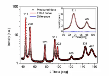
It should be noted that the crystallite size is often smaller than the grain size determined by microscopic methods. This difference can be explained by the fact that lattice defects inside the grains can break the coherency of X-rays. For instance, low-angle grain boundaries consisting of dislocations fragment grains into small diffraction domains and the size of these domains (crystallites) is measured by XLPA. The details of the eCMWP procedure can be found in Refs. 13 and 14. Because of the nano- grained microstructure of the studied samples, the physical broadening of the profiles was much higher than the instrumental broadening. Therefore, instrumental correction did not need to be applied in the evaluation. As an example, Fig. 1 shows eCMWP fitting for the sample SAA.
Fig. 1: eCMWP fitting of the X-ray diffraction pattern in a logarithmic intensity scale for the electrolyte side of sample SAA. The open circles and the solid line represent the measured data and the fitted curve, respectively. The inset displays a magnified part of the diffractogram in a linear intensity scale where the difference between the measured and the fitted patterns is also given at the bottom of the image.
2.4. Transmission electron microscopy
The microstructure was also investigated by transmission electron microscopy (TEM) using a Philips CM20 transmission electron microscope operated at an acceleration voltage of 200 kV. TEM images were taken in both planar and cross-sectional views. In the case of planar views, thinning to electron transparency was achieved by Ar+ ion-beam milling using a Technoorg Linda ionmill started with 10 keV Ar+ ion energy and ended with 3 keV, in order to minimize the ion-induced structural changes in the remaining surface layers [15]. For cross-sectional sample preparation, the sample was inserted between two pieces of silicon crystal, making a sandwich. This sandwich was installed into a titanium ring and fixed with a glue. Then, the sample was thinned by mechanical polishing and dimpling. The electron transparency was achieved by Ar+ ion-beam milling similar to the preparation of the planar view samples described above. A detailed description of the cross-sectional sample preparation can be found in Ref. 4. The estimated temperature of the sample during the process was not more than 180 °C, therefore no structural changes were expected [16]. In order to achieve a combination of good resolution and high number of studied grains, images were taken with a magnification of 50000. The number of the evaluated grains was about 1000 for each side (electrolyte or substrate side) and view (plane or cross-sectional view). The selected area electron diffraction (SAED) patterns were processed by the program “Process Diffraction” [17,18]. Selected area aperture was used to reduce the investigated sample area to 1 micrometer.
In the evaluation of the experimental grain size distribution, a log-normal distribution was assumed. First, the mean (<x>) and the standard deviation (SD) of the distribution were determined from the grain size histograms. Then, the median (m) and the square root of the log-normal variance (σ) were calculated from <x> and SD using the following formulas:
2 / 1
2 1
+
x x SD
= m
2
(2a)
2 / 2 1
1 ln
+
x
= SD
σ . (2b)
In order to check the validity of this procedure, we introduced two characteristic parameters for the measurement of the degree of the log-normal character of the grain size distribution. The first one is the relative difference between the median of the grain size values determined directly from the histograms (mx)and the median obtained with the assumption of the log-normal character of the size distribution (m in eq. (2a)):
x x
m m
= m
δ
. (3)
The average δ value for the different samples studied in this work was 2.6 % which indicates that the assumption of log-normal distribution for the grain size is a good approximation.
The second characteristic parameter was the probability of the assumption that the grain size distribution follows a log-normal distribution with the corresponding median (m) and square root of variance (σ) values. The test was carried out with Pearson's chi-square method [19]. This probability averaged for the studied samples has a high value of 92% which also indicates that the grain size distributions determined by TEM can be described well by log-normal functions.
2.5. Hardness tests
For Vickers microhardness tests, the samples were fixed on a steel stage. The tests were performed with a Zwick/Roell ZHμ indenter, using a load between 10 and 50 grams. A higher load was used for the harder samples to keep the indent diagonal nearly at a constant value of 10 µm. To avoid the hardness values to be affected by the sample stage, a common rule of thumb was used (according to ISO 6507 standard): the thickness of the sample must be at least 1.5 times larger than the average diagonal length of the indentation. The indentation diagonals were in the range of 7-12 μm, therefore
our samples were thicker (20 μm) than the required minimal sample thickness (11-18 μm). In Vickers geometry, the diagonal length of the indentation is approximately 7 times larger than the indentation depth; therefore, the indentation depth during the measurements was approximately 1-1.7 μm. Both the substrate and electrolyte sides were examined by hardness testing, and neither of them was polished to avoid any modification in the microstructures.
3. Results
3.1. Composition analysis
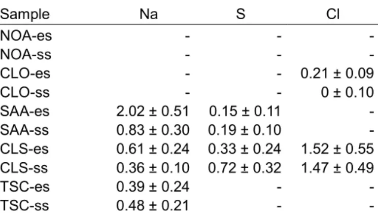
EDS analysis revealed that besides Ni three other elements were incorporated into the Ni layers:
sodium, sulfur and chlorine (the latter element only in samples deposited from nickel-chloride containing baths). The concentrations of sodium, sulfur and chlorine are listed for both the substrate and electrolyte sides of the five studied samples in Table 2. The codeposition of these elements is affected by the additives in the bath. Despite the fact that all of the applied electrolytes were based on nickel sulfate, the incorporation of sulfur in Ni layers was only detected for the samples deposited from baths containing saccharin (specimens SAA and CLS). This trend makes a microcavity-based solution entrapment unlikely. Rather, the sulfur incorporation can be explained by the decomposition of the saccharin which acts as sulfur source in accordance with the following reaction [20]:
C6H4[-CO-NH-SO2-] + Ni2+ + 8e- + 6H+ = NiS + C6H5-CO-NH2 + 2H2O. (4)
In the above equation, NiS indicates the interstitial sulfur impurity and has nothing to do with crystalline nickel sulfide grains that were not detected at all.
Similarly, although both the sulfate and Watts baths contained sodium ions (see Table 1), samples NOA and CLO do not contain sodium (see Table 2). Sodium absorption was observed only in the presence of the additive saccharin (specimens SAA and CLS). In the case of the sample TSC, trisodium citrate was the Na source, while for the specimens SAA and CLO, saccharin promoted Na incorporation. The chlorine in the samples CLO and CLS was provided by the nickel-chloride in the Watts bath.
Table 2: Concentration of Na, S and Cl in at.% determined by EDS for the electrolyte (es) and substrate (ss) sides of the samples.
Sample Na S Cl
NOA-es - - -
NOA-ss - - -
CLO-es - - 0.21 ± 0.09
CLO-ss - - 0 ± 0.10
SAA-es 2.02 ± 0.51 0.15 ± 0.11 - SAA-ss 0.83 ± 0.30 0.19 ± 0.10 - CLS-es 0.61 ± 0.24 0.33 ± 0.24 1.52 ± 0.55 CLS-ss 0.36 ± 0.10 0.72 ± 0.32 1.47 ± 0.49
TSC-es 0.39 ± 0.24 - -
TSC-ss 0.48 ± 0.21 - -
3.2. Grain size distributions and texture
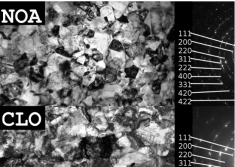
Figure 2 shows TEM images together with the corresponding SAED patterns obtained on Ni layers deposited from the two organic additive-free electrolytes NOA and CLO. The median, the square root of the log-normal variance and the mean of the grain size distribution obtained for the substrate and electrolyte sides by plane-view and cross-sectional TEM investigations are listed in Table 3. It can be seen that CLO has a slightly larger grain size than NOA. Large differences between the substrate and electrolyte sides as well as between the cross-sectional and plane views were not observed. For samples NOA and CLO, the TEM grain size is larger than the crystallite size determined by XLPA by a factor between 2 and 4 (see Table 3). This is a well-known phenomenon in the literature [4,6-8,21- 23] which is caused by the fragmentation of grains into smaller subgrains with slight misorientations which do not cause measurable contrast differences in the TEM images but could be noticed by XLPA as the latter method is very sensitive to small misorientations [8].
Figure2:Brightfield TEM images in plane view and the corresponding SAED patterns for the samples deposited from baths without organic additives: NOA (top) and CLO (bottom), with both images taken at the electrolyte side.
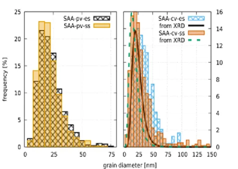
Plane-view TEM images for the samples with organic additives (SAA, CLS and TSC) are shown in Figs. 3 and 4. As an example, Fig. 5 shows the grain size distributions obtained for the substrate and electrolyte sides of the sample SAA. The median, the square root of the log-normal variance and the mean of the grain size distributions determined for the substrate and electrolyte sides are listed in Table 3. It can be seen that neither TEM grain nor XRD crystallite size changed significantly due to the addition of trisodium citrate as compared to sample NOA. At the same time, saccharin yielded a considerable grain refinement: samples SAA and CLS exhibited much smaller grain sizes of about 20 nm than for the additive-free specimens NOA and CLO.
Fig. 3: Bright-field TEM images in plane view and the corresponding SAED patterns, taken at the electrolyte side for the samples deposited from baths containing saccharin as organic additive: SAA (top) and CLS (bottom). Note the numerous, almost continuous diffraction rings in the SAED patterns, revealing the much finer grain structure in comparison with the additive-free samples (cf. Fig. 2).
Fig. 4: Bright-field TEM image in plane view and the corresponding SAED pattern for sample TSC, taken at the electrolyte side.
Fig. 5: Grain size distributions evaluated from the TEM images of the sample SAA. At left, plane-view data at electrolyte and substrate sides are displayed. At right, cross-sectional view data are shown and compared with XLPA crystallite size distribution.
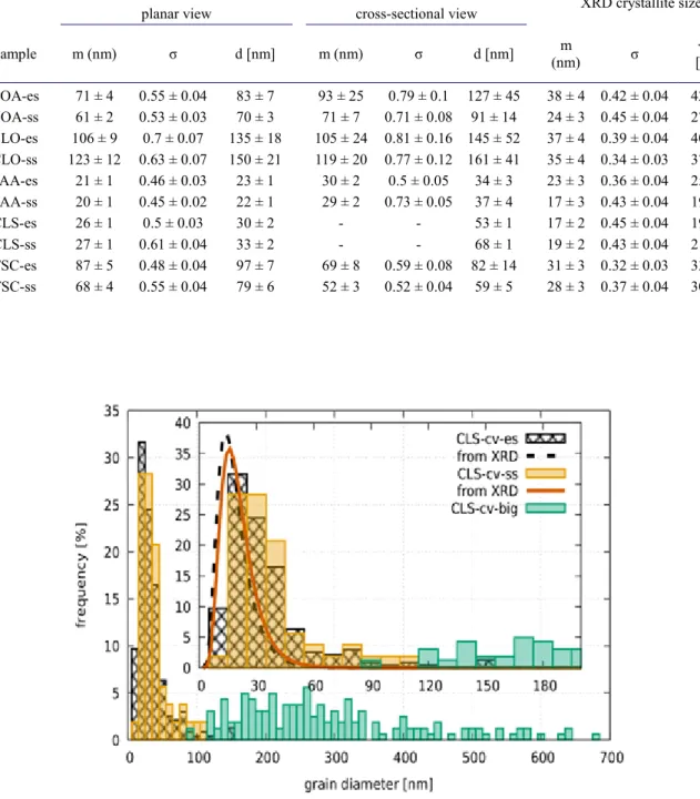
Figures 6-8 show cross-sectional TEM images for samples SAA, TSC and CLS. The grain size distributions obtained from the cross-sectional and plane-view images agree well for specimens SAA and TSC. At the same time, for specimen CLS large grains with the size of 100-600 nm are embedded in the fine-grained matrix which has an average grain size of ~30 nm. The number of the large grains decreases with increasing the distance from the substrate side of the layer. Due to their low number, the sizes of these grains were evaluated from TEM images with a magnification of 8800x. As a result of the embedded large grains, the grain size distribution has a bimodal character as shown in Fig. 9.
The bimodal grain size distribution may be the result of the combined coarsening and refining effects of nickel-chloride and saccharin, respectively. It should be noticed that the plane-view image in Fig. 3 does not show large grains which is most probably due to the smaller picture size compared to the cross-sectional image in Fig. 9. Accidentally, the area studied in the plane-view image was free of large grains. It is also noted that for sample CLS the crystallite size distribution determined by XLPA was not affected by the bimodality revealed by TEM. Most probably, the large grains are fragmented into subgrains which act as crystallites in the XLPA evaluation. In accordance with the generally accepted definition, the grains are separated from their neighbors by high-angle grain boundaries therefore they have significantly different contrasts in the TEM images. At the same time, the subgrains inside the grains are bounded by low-angle grain boundaries, thus the small misorientation between them may cause only slight contrast differences. However, XLPA is very sensitive to small misorientations, therefore the crystallite size obtained by this method often shows good agreement with the subgrain size [8].
Fig. 8: Cross sectional bright-field (left) and dark-field (right) TEM images for sample CLS. The bright- field and dark-field sides were composed from two images taken at the substrate and electrolyte sides. The arrow indicates the growth direction of the layer.
Fig. 6: Cross-sectional TEM image and the corresponding SAED pattern for sample SAA, taken at the substrate side. The arrow indicates the growth direction of the layer.
Fig. 7: Cross-sectional TEM image for sample TSC taken near to the substrate side. The arrow indicates the growth direction of the layer.
Table 3: The median (m), the square root of the lognormal variance (σ) and the mean of the grain size (d) and crystallite size (<x>) distributions obtained by TEM and XLPA, respectively. Both the electrolyte (es) and substrate (ss) sides of the samples were investigated. For the planar view of the specimen CLS, the values of m and σ are not shown due to the bimodal nature of the grain size distribution (see the text).
TEM grain size
XRD crystallite size
planar view cross-sectional view
Sample m (nm) σ d [nm] m (nm) σ d [nm] m
(nm) σ <x>
[nm]
NOA-es 71 ± 4 0.55 ± 0.04 83 ± 7 93 ± 25 0.79 ± 0.1 127 ± 45 38 ± 4 0.42 ± 0.04 42 ± 5 NOA-ss 61 ± 2 0.53 ± 0.03 70 ± 3 71 ± 7 0.71 ± 0.08 91 ± 14 24 ± 3 0.45 ± 0.04 27 ± 3 CLO-es 106 ± 9 0.7 ± 0.07 135 ± 18 105 ± 24 0.81 ± 0.16 145 ± 52 37 ± 4 0.39 ± 0.04 40 ± 5 CLO-ss 123 ± 12 0.63 ± 0.07 150 ± 21 119 ± 20 0.77 ± 0.12 161 ± 41 35 ± 4 0.34 ± 0.03 37 ± 5 SAA-es 21 ± 1 0.46 ± 0.03 23 ± 1 30 ± 2 0.5 ± 0.05 34 ± 3 23 ± 3 0.36 ± 0.04 25 ± 2 SAA-ss 20 ± 1 0.45 ± 0.02 22 ± 1 29 ± 2 0.73 ± 0.05 37 ± 4 17 ± 3 0.43 ± 0.04 19 ± 4 CLS-es 26 ± 1 0.5 ± 0.03 30 ± 2 - - 53 ± 1 17 ± 2 0.45 ± 0.04 19 ± 3 CLS-ss 27 ± 1 0.61 ± 0.04 33 ± 2 - - 68 ± 1 19 ± 2 0.43 ± 0.04 21 ± 3 TSC-es 87 ± 5 0.48 ± 0.04 97 ± 7 69 ± 8 0.59 ± 0.08 82 ± 14 31 ± 3 0.32 ± 0.03 33 ± 3 TSC-ss 68 ± 4 0.55 ± 0.04 79 ± 6 52 ± 3 0.52 ± 0.04 59 ± 5 28 ± 3 0.37 ± 0.04 30 ± 4
Fig. 9: Grain size distributions for the sample CLS evaluated from the TEM images taken in cross-sectional view. Electrolyte and substrate side TEM data are given and compared with the XLPA crystallite size distributions. In addition, the distribution of the larger grains is also shown.
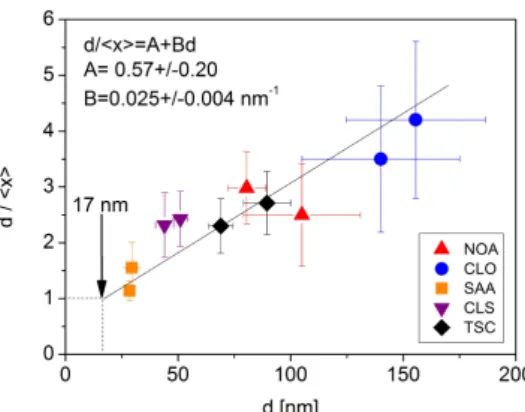
Fig. 10: The ratio of the grain (d) and crystallite (<x>) sizes determined by TEM and XLPA, respectively, as a function of the TEM grain size.
A general observation was that the ratio of the grain and crystallite sizes obtained by TEM and XLPA decreases with decreasing the grain size as shown in Fig. 10. The grain size was taken as the average of the sizes determined from the plane-view and cross-sectional images. A straight line was fitted to the data points in Fig. 10. This result revealed that the ratio between the grain and crystallite sizes varied between 1 and 4 and this ratio increased with increasing the grain size. Thus, the larger the grain size, the higher the number of crystallites per grain. Extrapolating to dx = 1 , a critical grain size of ~17 nm was obtained (see Fig. 10), which suggests that below this size limit the grain size agrees with the crystallite size due to the lack of subgrain structure.
Both X-ray and electron diffraction experiments revealed that the majority of the studied samples exhibit a crystallographic texture. Figure 11 shows X-ray pole figures of reflection (220) for the specimens NOA, CLO, SAA and CLS. It is revealed that the additive-free samples NOA and CLO have a strong (220) out-of-plane texture. The addition of saccharin to the basic electrolytes resulted in the suppression of texture in samples SAA and CLS. Fig. 11(d) suggests that sample CLS has a weak (10%) remaining (220) texture. Figure 12 reveals that sample TSC has a strong (200) out-of-plane texture.
Fig. 11: Pole figures for reflection (220) taken on the electrolyte sides of samples NOA (a), CLO (b), SAA (c), CLS (d). It is revealed that additive saccharin inhibits the formation of the strong (220) out-of-plane texture.
Fig. 12: Pole figures for reflections (200) and (220) taken on the electrolyte side of sample TSC. The pole figures indicate strong (200) out of plane texture.
3.3. Dislocations and twin faults
XLPA determined the defect densities for both substrate and electrolyte sides of the five studied layers. The dislocation density and the twin fault probability values are listed in Table 4. The twin fault probability (β) in percentage can also be evaluated from the TEM images as the ratio of the spacing between planes (111) in Ni (d111 =0.2034 nm) and the average width of the twinned regions in the grains (dtwin ):
100%
111 dtwin
= d
β .
(5)
The values of β determined by TEM are also listed
in Table 4. The twin fault probability values determined by XLPA and TEM show a good agreement except for the specimen SAA. For this specimen, XLPA shows very high values of β and TEM revealed a slightly lower twin fault probability than XLPA. This difference can be explained by the presence of nanotwins which contribute to β determined by XLPA but can hardly be measured by TEM [4]. In addition, the reliability of XLPA in the determination of β is higher than that for TEM as XLPA has six orders of magnitudes larger inspected volume than TEM. Some of the twin boundaries can be observed on Fig. 13 as an example.
Fig. 13: Bright-field TEM image in plane view for the sample deposited from bath containing saccharin as organic additive (SAA) taken at the electrolyte side. Arrows indicate some of the twin boundaries. It has to be noted, that grains which contain twin boundaries are typically larger than the average [4]
Table 4: The dislocation density (ρ) from XLPA and the twin fault probability (β) evaluated by XLPA and TEM for the electrolyte (es) and substrate (ss) sides of the samples.
Sample ρ (1014 m-2) β (%)
XRD TEM XRD
NOA-es 12 ± 1 - - NOA-ss 14 ± 2 - -
CLO-es 12 ± 1 0.4 ± 0.3 0.2 ± 0.1
CLO-ss 8 ± 1 - -
SAA-es 164 ± 16 1.6 ± 0.4 3.6 ± 0.1 SAA-ss 163 ± 25 1.8 ± 0.5 3.2 ± 0.3 CLS-es 98 ± 10 1.8 ± 0.6 2.0 ± 0.1 CLS-ss 105 ± 11 1.6 ± 0.6 2.3 ± 0.1 TSC-es 32 ± 3 - -
TSC-ss 21 ± 2 - -
The organic-additive-free sulfate-based (NOA) and nickel-chloride-containing Watts bath (CLO) samples have the lowest dislocation density with the values of about ~ 10 × 1014 m-2 (see Table 4).
Moreover, zero or very low twin fault probability values were observed in the microstructure. The addition of trisodium citrate to the bath (sample TSC) yielded an increase of the dislocation density by a factor of about two; however, it did not result in considerable twin fault formation. The layers deposited using saccharin (samples SAA and CLS) have the largest probability of twin faults (2-3.6 %) and also contain an extremely high dislocation density of 100-160 × 1014 m-2. In addition, a significant difference between the substrate and electrolyte sides was not observed, indicating a high level of homogeneity of the microstructure along the growth direction for these layers.
3.4. Hardness
The hardness values obtained for the substrate and electrolyte sides of the layers are listed in Table 5. The lowest hardness values were obtained on the additive-free samples NOA and CLO (HV = 2000-3000 MPa). The addition of trisodium citrate to the bath (sample TSC) yielded an increase of the hardness to ~3800 MPa. The highest hardness values of ~5900 MPa were obtained for the layer deposited from the sulfate-type bath with saccharin (sample SAA) due to the very small grain size and the large defect densities (dislocations and twin faults). The addition of saccharin to the Watts-type bath resulted in a smaller hardness (4500-4600 MPa) due to the embedded coarse grains (see Fig. 9).
Table 5: The Vickers hardness (HV) determined for the electrolyte (es) and substrate (ss) sides of the samples.
Sample HV (MPa) NOA-es 1877 ± 211 NOA-ss 2837 ± 344 CLO-es 2874 ± 363 CLO-ss 3031 ± 353 SAA-es 5961 ± 808 SAA-ss 5887 ± 945 CLS-es 4487 ± 363 CLS-ss 4700 ± 793 TSC-es 3713 ± 504 TSC-ss 3794 ± 377
4. Discussion
4.1 Influence of bath composition on the grain size and texture
The basic mechanism of electrodeposition is the following: metal ions attach one by one to the surface of the cathode substrate which may result in (i) an extension of the existing grains (crystal growth) or (ii) a formation of a new grain (nucleation). Basically, the ratio of these two competitive processes determines the crystallite size since at low temperatures the coalescence of crystallites is negligible.
Since the equilibrium potential of nickel(II)/nickel redox system, E0(Ni2+/Ni), is more negative than that of hydrogen, nickel electrodeposition is always accompanied by simultaneous hydrogen evolution (or hydrogen codeposition) at the cathode surface. Since the applied current density was far from the diffusion-limited conditions, hydrogen had no effect on the metal deposition rate. However, adsorbed hydrogen atoms decrease the surface energy of metal deposits [24,25], which has an effect on the texture formation.
Due to the surface energy anisotropy of nickel, the different crystal planes grow at different rates, thereby causing texture. The order of formation rate of crystalline planes in face-centered cubic (fcc) Ni is (111)>(100)>(110) [24]. On the other hand, quantum mechanical calculations [25-27] proved that different lattice planes have different hydrogen adsorption rate, therefore different hydrogen coverage.
The lower the planar density of a crystal plane, the higher the hydrogen adsorption rate and the faster the decrease of surface energy. Thus, the effect of hydrogen codeposition on the growth rate of lattice planes decreases in the order of (110)>(100)>(111). As a result of this effect, even at a low current density, a (220) texture forms in nickel due to hydrogen codeposition. As samples NOA and CLO exhibited (220) texture (see Figure 12), in these specimens the texture formation is most probably controlled by the hydrogen evolution.
Foreign atoms and molecules also have an effect on the texture in different ways. They influence the total overpotential and can change the texture determined by the surface anisotropy energies and hydrogen codeposition as discussed above. For instance, trisodium citrate decreases the rate of hydrogen gas detachment [28]. Sodium adsorbed from trisodium citrate, similarly to potassium, has a strongly selective effect on the surface energies of crystal planes [29]. These two effects could turn the texture into direction (200) as it was observed in the case of sample TSC.
Sulfur adatoms also have an effect on the texture in Ni films. As shown in section 3.1, the incorporated sulfur originates from saccharin through the formation of NiS and benzamide [19]. The strong Ni-S covalent bond and its preferred bonding angles [30] can increase the probability of grain boundary formation, thereby contributing to the grain refinement and the reduction of texture. In addition, quantum mechanical calculations proved that during coadsorption of S and H, the adsorption of S at a three-fold site on plane (111) in Ni has a tendency to block the adsorption of H at the nearby surface sites [31], thus suppressing the texture-increasing effect of hydrogen codeposition.
Consequently, sulfur has a tendency to assist the formation of a texture-free, nano-grained nickel structure as it was observed in samples deposited from solutions containing saccharin as a sulfur source (in the cases of the specimens SAA and CLS). Although these quantum mechanical calculations assume perfectly flat crystalline surfaces, the effect of sulfur on the hydrogen codeposition may occur even if sulfur is absorbed at kinks or edges.
According to former studies [4,32], all additives have a common effect on the nucleation and grain growth rate: additives with a hydrophilic functional group can form an “organic shield” between the water in the electrolyte solution and the deposited metal surface, especially at the kink sites and step edges, thereby hindering the ion transfer, but not blocking the electron transfer. Since these crystal sites are the most active parts during grain growth, the ratio of nucleation and grain growth increases and grain refinement occurs. As there is no epitaxial relationship between the old and the newly formed grains, this shielding mechanism inhibits the development of texture as well.
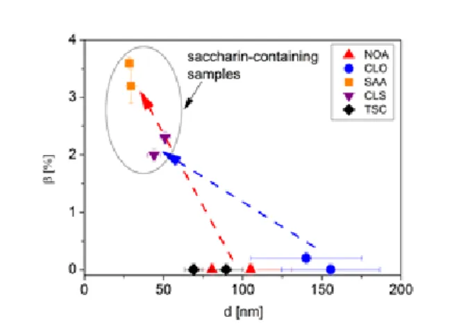
Fig. 14: The twin fault probability (β) versus the grain size (d). The grain size was calculated as the average of the size values determined from the plane- and cross- view images. Dashed arrows indicate the difference between the corresponding saccharin-free and saccharin-containing samples.
Fig. 15: The dislocation density (ρ) as a function of the grain size. The grain size was calculated as the average of the size values determined from the plane- and cross-view images.
Dashed arrows indicate the difference between the corresponding saccharin-free and saccharin- containing samples.
4.2. The effect of additives on twin faults and dislocations
Table 4 shows that significant twin fault probability was detected in the samples CLO, SAA and CLS.
Twin faults have the lowest energy among the grain boundaries in fcc materials, therefore it is energetically favorable if the growing grains in the deposited Ni films are separated by twin boundaries. Statistically, if a constant fraction of twin boundaries is assumed in the grain boundary distribution, the smaller the grain size, the higher the amount of twin boundaries. Figure 14 shows the twin fault probability determined by XLPA as a function of grain size. The grain size was calculated as the average of the size values determined from the plane-view and cross-sectional TEM images.
Indeed, the highest twin fault probabilities were detected in the samples having the smallest grain size, although there is no strict correlation between the twin fault probability and the grain size. The arrows in Fig. 14 indicates that the addition of saccharin resulted in a large increase in twin fault probability for both the sulfate-type and Watts-type baths. The increased rate of twin fault formation may be partly due to the preferred adsorption sites of sulfur: both experimental [33-35] and theoretical [30,31]
results demonstrated that S is usually adsorbed in the three-fold fcc hollow sites on (111) surfaces in Ni. Let us denote the fcc stacking of (111) planes as …ABCABCABC.... Then, we can imagine that the sulfur atoms occupy a layer C while layers A and B (and other C layers) contain only Ni atoms.
Then, the following sequence of (111) planes forms: …ABCABCABCS.... where CS indicates a layer C containing sulfur atoms. According to the results of different experimental and theoretical studies [33,34,36-39], the distance between the absorbed S atoms and the (111) surface is smaller by 10-30%
than the ordinary distance between (111) planes in a perfect Ni crystal. Due to this decreased layer spacing, the electron orbits of NiB-S and S-NiA bonds (where NiB-S represents the bond between an S atom in the CS layer and a Ni atom in the B layer before the CS layer and S-NiA represents the bond between an S atom in the CS layer and a Ni atom in the A layer after the CS layer in the layer sequence) can interact with each other and a local hexagonal close-packed (hcp) stacking (i.e., stacking BCB) is more favorable [40]. When the BCB layer stacking was formed, the long-range fcc order is restored and a twin fault forms in accordance with the sequence …ABCABCSBACBA.... This effect results in an increase in twin fault probability for the samples containing sulfur. It is noted that sulfur may occupy any layer from planes A, B and C, and in the description given above layer C was selected arbitrarily. After a few layers, there is no reason for sulfur to occupy a layer C again. For example, two twin faults can be formed by substituting Ni atoms by sulfur in layers A and C, resulting in the following sequence: …ABCABCSBACBASBCABC...
As shown in Table 4, the additives increased the dislocation density. As the interiors of nanograins usually do not store dislocations [41], the majority of dislocations is assumed to be located in the grain/subgrain boundaries. These dislocations may form in order to reduce the elastic
incompatibility stresses developed between the grains/subgrains at their boundaries. Therefore, the smaller grain size is expected to be accompanied by an increased dislocation density. Indeed, Fig. 15 shows that although there is a scattering in the data points, the dislocation density scales fairly well with the grain size. It should be noted, however, that there is no strict correlation between the grain size and the dislocation density. For samples NOA and TSC, the grain sizes are only slightly different while the dislocation density in the latter sample is 2-3 times larger (see Table 4). It should be noted that in Fig. 15 the grain size was taken as the average of the sizes determined from the plane-view and cross-sectional images. The smallest grain size and the highest dislocation density were achieved in the layer deposited from the sulfate-type bath containing saccharin (sample SAA). The arrows in Fig.
15 indicate that saccharin addition was more effective in the increase of the dislocation density for the samples deposited from the sulfate-type bath than for the layer grown from the Watts electrolyte.
4.3. Change of the hardness due to the additives
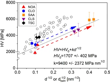
The hardness test results (see Table 5) suggest that the Vickers hardness is in accordance with the grain size and the defect density. Generally, the samples deposited from the additive-free sulfate-type and Watts electrolytes (specimens NOA and CLO) were the softest samples (HV = 2000-3000 MPa) corresponding to the largest grain sizes and the lowest dislocation densities. Although the specimen grown from the trisodium-citrate based electrolyte (specimen TSC) had nearly the same grain size as sample NOA, it showed higher hardness (~3800 MPa) due to the larger dislocation density. The samples deposited using saccharin (specimens SAA and CLS) had the highest hardness values, due to the combined effect of grain refinement and the increase of defect density (both dislocations and twin faults). Sample SAA was the hardest sample (~5900 MPa), while sample CLS had a smaller hardness value (4500-4600 MPa) in accordance with the bimodal nature of the microstructure caused by the combined effect of nickel-chloride and saccharin. Assuming that the grain boundaries have a major contribution to the strength of the studied Ni films, the hardness was plotted as a function of the inverse square root of the grain size in Fig. 16 (Hall-Petch plot). During this analysis, the twin boundaries were also considered as grain boundaries, therefore when the average twin spacing determined from eq. (5) was smaller than the grain size, the former quantity was used in the Hall- Petch plot. The linear fit on the data points yielded the following relationship:
2 / 1 0
d
k + HV
=
HV , (6)
where HV0 = 1707 ± 402 MPa and k = 9400 ± 2372 MPa·nm1/2. The scattering of the data points around the best fit line can be explained by the various strengthening effects of dislocations and impurities in the different samples. It can be concluded that the addition of saccharin to the sulfate- type bath resulted in a larger increase of hardness than in the case of Watts-type electrolyte.
Fig. 16: Hall-Petch plot for the hardness (HV) versus the inverse square root of the grain size (d). If the twin fault spacing (dtwin) was smaller than the grain size for a sample, the former quantity was used in the Hall-Petch plot. Dashed arrows indicate the increase of the hardness due to the addition of saccharin.
The open circles show the hardness values determined formerly on electrodeposited Ni layers in the literature (see Refs. [43-49]).
Figure 16 also shows hardness data for electrodeposited Ni films studied formerly in the literature [42-48]. In these investigations, the grain size was also determined from TEM images similar to our study, however without considering the strengthening effect of twin boundaries. For large grain sizes (i.e., for small d-1/2 values), there is a relatively good agreement between the hardness values obtained in the present study and the literature. At the same time, with decreasing the grain size a deviation is revealed between the data determined in the present investigation and the former studies.
The difference is caused by the fact that in the present study the strengthening effect of twin boundaries was also taken into account by substituting the grain size with the twin boundary spacing (dtwin) in the Hall-Petch equation. As high twin fault probability was detected in the samples with small grain sizes, therefore this modification was more pronounced for large d-1/2 values. It should be noted that twin faults inside the grains have similar strengthening effect as the other grain boundaries [49], therefore the modification of Hall-Petch plot in the present study was reasonable.
5. Conclusions
The effect of additives (saccharin and trisodium citrate) on the microstructure of electrodeposited nanocrystalline Ni films produced from sulfate-based electrolytes was investigated. In addition, the combined effect of nickel-chloride and saccharin was also investigated for a film deposited in a Watts bath. The following conclusions were drawn from the results:
1. In the films deposited without organic additives, a grain size of ~70-160 nm was observed without considerable twinning. In addition, a crystallographic texture was detected where the planes (220) were parallel to the film surface. The organic additive saccharin eliminated the texture, yielded fine-grained microstructures (~20-100 nm) and increased the density of lattice defects (dislocations and twin faults). The efficiency for grain refinement of saccharin as additive was larger for the sulfate- type bath than for the Watts electrolyte.
2. It was found that the addition of nickel-chloride to the electrolyte (Watts bath) increased the grain size. The combined effect of nickel-chloride and saccharin led to a bimodal grain size distribution. Trisodium citrate did not result in a considerable grain refinement but increased the dislocation density. Although there was no strict correlation between the dislocation density and the grain size, the highest dislocation densities were observed for the samples having the smallest grain sizes in the studied Ni films. These specimens were processed from saccharin-containing electrolytes.
3. It was found that in addition to the small grain size, the incorporating sulfur was also responsible for the enhanced formation of twin faults in the samples processed from saccharin- containing baths. It was proposed that the formation of twin boundaries was partly due to the sulfur codeposition on (111) planes during electrodeposition.
4. The samples deposited from the additive-free sulfate-type and Watts-type baths exhibited similar hardness values (2000-3000 MPa). The layer grown from the trisodium-citrate based electrolyte showed higher hardness (~3800 MPa) due to the larger dislocation density. Saccharin yielded the largest hardness values due to the superimposed effect of the grain refinement and the increase of defect density (both dislocations and twin faults). The highest hardness was achieved for the sample deposited from the sulfate-type bath with saccharin additive (~5900 MPa). The combined effect of nickel chloride and saccharin yielded a smaller hardness value (4500-4600 MPa) in accordance with the bimodal nature of the microstructure.
Acknowledgements
This work was financially supported by the Hungarian Scientific Research Fund, OTKA, Grant Nos.
K-109021 and PD-121049.
References
[1]
M.J. Aus, B. Szpunar, A.M. EI-Sherik, U. Erb, G. Palumbo, K.T. Aust, Magnetic properties of bulk nanocrystalline nickel, Scripta Metall. Mater. 27 (1992) 1639-1643.[2]
I. Bakonyi, E. Tóth-Kádár, T. Tarnóczi, L.K. Varga, Á. Cziráki, I. Gerőcs, B. Fogarassy, Structure and properties of fine-grained electrodeposited nickel, Nanostruct. Mater. 3 (1993) 155-161.[3]
U. Erb, A.M. El-Sherik, G. Palumbo, K.T. Aust, Synthesis, structure and properties of electroplated nanocrystalline materials. Nanostruct. Mater. 2 (1993) 383-391.[4]
T. Kolonits, P. Jenei, B.G. Tóth, Zs. Czigány, J. Gubicza, L. Péter, I. Bakonyi, Characterization of Defect Structure in Electrodeposited Nanocrystalline Ni Films, J. Electrochem. Soc. 2016 163(3): D107-D114; doi:10.1149/2.0911603jes[5]
M. Schlesinger, M. Paunovic, Modern Electroplating, Ch. 3.3.3, Wiley (2010)[6]
J. Gubicza, Defect Structure and Properties of Nanomaterials, 2nd and Extended Edition, Woodhead Publishing, Duxford, 2017.[7]
C. B. Carter, D. B. Williams, Transmission Electron Microscopy – Diffraction, Imaging and Spectrometry, Springer Science, 2016.[8]
T. Ungár, G. Tichy, J. Gubicza, R. J. Hellmig: Correlation between subgrains and coherently- scattering-domains, Powder Diffraction 20 (2005) 366-375.[9]
B.G. Tóth, L. Péter, Á. Révész, J. Pádár, I. Bakonyi, Temperature dependence of the electrical resistivity and the anisotropic magnetoresistance (AMR) of electrodeposited Ni-Co alloys, Eur.Phys. J. B 75 (2010) 167-177.
[10]
K.S. Kumar, S. Suresh, M.F. Chisholm, J.A. Horton, P. Wang, Deformation of electrodeposited nanocrystalline nickel. Acta Materialia 51 (2003) 387–405[11]
T.A. Green, A.E. Russell, S. Roy, The Development of a Stable Citrate Electrolyte for the Electrodeposition of Copper-Nickel Alloys. J: Electrochem. Soc. 150 (1998) 875-881.[12]
V. Weihnacht, L. Péter, J. Tóth, J. Pádár, Z. Kerner, C.M. Schneider, I. Bakonyi, Giant magnetoresistance in Co-Cu/Cu multilayers prepared by various electrodeposition control modes, J. Electrochem. Soc. 150 (2003) C507-C515; L. Péter, J. Pádár, E. Tóth-Kádár, Á.Cziráki, P. Sóki, L. Pogány, I. Bakonyi, Electrodeposition of Co-Ni-Cu/Cu multilayers. 1.
Composition, structure and magnetotransport properties, Electrochim. Acta 52 (2007) 3813- 3821.
[13]
G. Ribárik, J. Gubicza, T. Ungár, Correlation between strength and microstructure of ball-milled Al–Mg alloys determined by X-ray diffraction, Mater. Sci. Eng. A 387–389 (2004) 343-347.[14]
L. Balogh, G. Ribárik, T. Ungár, Stacking faults and twin boundaries in fcc crystals determined by x-ray diffraction profile analysis, J. Appl. Phys. 100 (2006) 023512/1-10[15]
Á. Barna, Topographic kinetics and practice of low angle ion beam thinning, Materials Research Society Symp. Proc. 254 (1992) 3-22.[16]
U. Klement, M. da Silva, G. Hibbard, Thermal stability of nanocrystalline Ni- and Co-based pulsed current electrodeposits: correlation of calorimetric measurements and microstructure development upon annealing, Transact. IMF, I 95 (2017) 20-24.[17]
J.L. Lábár, Electron Diffraction Based Analysis of Phase Fractions and Texture in Nanocrystalline Thin Films, Part II: Implementation", Microsc. Microanal. 15 (1) (2009), 20-29[18]
J. L. Lábár, Electron Diffraction Based Analysis of Phase Fractions and Texture in Nanocrystalline Thin Films, Part III: Application Examples, Microsc. Microanal. 18 (3) (2012), 406-420[19]
K. Pearson, X. On the criterion that a given system of deviations from the probable in the case of a correlated system of variables is such that it can be reasonably supposed to have arisen from random sampling, The London, Edinburgh, and Dublin Philosophical Magazine and Journal of Science Series 5, 50(302) (1900) 157–175.[20]
M. Kouncheva, G. Raichevski, St. Vitkova, The effect of sulphur and carbon inclusion on the corrosion resistance of electrodeposited Ni-Fe alloy coatings, Surf. Coat. Technol. 31 (1987) 137-142[21]
B. Akbari, M. Pirhadi Tavandashti, M. Zandrahimi, Particle size characterization ofnanoparticles – A practical approach, Iran. J. Mater. Sci. Eng. (2011) 48-56.
[22]
V. D. Mote, Y. Purushotham, B. N. Dole, Williamson-Hall analysis in estimation of lattice strain in nanometer-sized ZnO particles, Journal of Theoretical and Applied Physics 6:1 (2012) 1-6.[23]
T.C. Prathna, N. Chandrasekaran, Ashok M. Raichur, Amitava Mukherjee, Biomimetic synthesis of silver nanoparticles by Citrus limon (lemon) aqueous extract and theoretical prediction of particle size, Colloids and Surfaces B: Biointerfaces, 82(1) (2011) 152-159.[24]
A.K.N. Reddy, Preferred orientations in nickel electro-deposits I. The mechanism of development of textures in nickel electro-deposits, J. Electroanal. Chem. 6 (1963) 141-152.[25]
D.Y. Li, J.A. Szpunar, Textural evolution in electrodeposits under the influence of adsorbed foreign species: Part I Textural evolution in iron electrodeposits affected by hydrogen co- deposition, J. Mater. Sci. 32 (1997) 5513-5523.[26]
L. Kristinsdóttir, E. Skúlason, A systematic DFT study of hydrogen diffusion on transition metal surfaces, Surf. Sci. 606 (2012) 1400-1404.[27]
P. Ferrin, S. Kandoi, A. U. Nilekar, M. Mavrikakis, Hydrogen adsorption, absorption and diffusion on and in transition metal surfaces: A DFT study, Surf. Sci. 606 (2012) 679-689.[28]
X. Wu, Q. Gao, Z. Li, Effects of additives on morphology and hydrogen evolution activities of nickel films prepared by electrodepositing, Int. J. Electrochem. Sci. 10 (2015) 8823-8833.[29]
D.Y. Li, K. Osseo-Asare, Textural evolution in electrodeposits under the influence of adsorbed foreign species: Part II A simulation study on effects of potassium chloride on textural evolution in copper electrodeposits, J. Mater. Sci. 32 (1997) 5525-5532.[30]
M. Neurock and R. A. van Santen, Theory of carbon-sulfur bond activation by small metal sulfide particles, Journal of the American Chemical Society 116(10) (1994) 4427-4439[31]
H. Yang and J. L. Whitten, Adsorption of SH and OH and coadsorption of S, O and H on Ni(111), Surface Science 370 (1997) 136-154[32]
H. Natter, R. Hempelmann, Nanocrystalline copper by pulsed electrodeposition: the effects of organic additives, bath temperature, and pH, J. Phys. Chem. 100 (1996) 19525-19532.[33]
J.E. Demuth, D.W. Jepsen, P. M. Marcus, Crystallographic dependence of chemisorption bonding for sulfur on (001), (110), and (111) nickel, Phys. Rev. Letter 32(21) (1974) 1182-1185[34]
Th. Fauster, H. Durr, D. Hartwig, Determination of the geometry of sulphur on nickel surfacesby low-energy ion scattering, Surface Science 178 (1986) 657-666
[35]
D.R. Mullins, D.R. Huntley, T. Tang, D. K. Saldin, W. T. Tysoe, The adsorption site and orientation of CH3S on Ni (111), Surface Science 380 (1997) 468-480[36]
Y.K. Wu, K.A.R. Mitchell, A refined LEED structural determination for the surface designated Ni (111)–(2 × 2)–S, Canadian Journal of Chemistry, 67(11) (1989) 1975-1979[37]
D.R. Warburton, P.L. Wincott, G. Thornton, F.M. Quinn, D. Norman, Incorporation of sulphur into the (111) surface of nickel?, Surf. Sci. 211/212 (1989) 71-81[38]
Y. Kitama, T. Yokoyama, T. Ohta, M. Funabashi, N. Kosugi, H. Kuroda, Surface EXAFS and XANES studies of (53×2)S/Ni(111): A pseudo-c(2×2)S/Ni(100) model with surface reconstruction, Surf. Sci. 214 (1989) L261-L269[39]
Y.S. Ku, S.H. Overbury, Structure analysis of S adsorbed on Ni(111) by low energy Li+ ion scattering, Surf. Sci. 276 (1992) 262-272[40]
J.M. Tyler, J.L. Fry, Energy Bands of Hexagonal NiS, Physical Review B 1(12) (1970) 4604- 4616[41]
M. Dao, L. Lu, R.J. Asaro, J.T.M. De Hosson, E. Ma, Toward a quantitative understanding of mechanical behavior of nanocrystalline metals, Acta Mater. 55 (2007) 4041-4065.[42]
A.M. El-Sherik, U. Erb , G. Palumbo, K.T. Aust, Deviations from hall-petch behaviour in as- prepared nanocrystalline nickel, Scripta Metall. Mater. 27 (1992) 1185-1188.[43]
D.H. Jeong, F. Gonzalez, G. Palumbo, K.T. Aust, U. Erb, The effect of grain size on the wear properties of electrodeposited nanocrystalline nickel coatings, Scripta mater. 44 (2001) 493-499.[44]
J.X. Kang, W.Z. Zhao, G.F. Zhang, Influence of electrodeposition parameters on the deposition rate and microhardness of nanocrystalline Ni coatings, Surf. Coat. Technol. 203 (2009) 1815- 1818.[45]
A. Godon, J. Creus, S. Cohendoz, E. Conforto, X. Feaugas, P. Giraulta, C. Savalla, Effects ofgrain orientation on the Hall–Petch relationship in electrodeposited nickel with nanocrystalline grains, Scripta Mater. 62 (2010) 403-406.