DEVELOPMENT, TESTING AND APPLICATION OF LAMINAR MULTIELECTRODES AND
BIOCOMPATIBLE COATINGS FOR INTRACORTICAL APPLICATIONS
Ph.D. dissertation
László Bálint Grand
Scientific advisors:
Prof. György Karmos, M.D., Ph.D.
István Ulbert, M.Sc., M.D., Ph.D.
Interdisciplinary Technical Sciences Doctoral School Faculty of Information Technology
Pázmány Péter Catholic University Budapest 2010
DOI:10.15774/PPKE.ITK.2010.004
To my loving parents, family and friends.
DOI:10.15774/PPKE.ITK.2010.004
DEVELOPMENT, TESTING AND APPLICATION OF LAMINAR MULTIELECTRODES AND BIOCOMPATIBLE
COATINGS FOR INTRACORTICAL APPLICATIONS
by László Bálint Grand Abstract
Simultaneous observation of the activity of a large number of cells might be the key factor for a better understanding of neuronal systems [1]. Modus operandi of different neuronal networks, communication between various neuronal populations and functional connectivity between different brain areas can be uncovered by using simultaneous multisite recording techniques [2-5]. Within the frame of my dissertation, I present the design process, manufacturing and testing of a novel multichannel extracellular silicon microprobe for research applications. Since the utility of an implanted neural interface depends crucially on its biocompatibility and long term viability I addressed this question by investigating the short and long-term effects of various coatings on foreign body reactions emerging around implanted silicon microprobes. Multielectrodes that can be implanted into the central nervous system for long-term are essential tools to study physiological processes at the population level and to elucidate complex brain mechanisms. To prove the advantages of using multichannel cutting edge neural interfaces in basic research I lead the reader by the hand through a case study in which I reveal how I investigated the bioelectric signals of acoustic information processing recorded from the cat auditory cortical layers in different states of the natural sleep-wake cycle and during anesthesia by using a chronically implantable multielectrode array.
The research projects presented in my dissertation unite an engineer’s innovations with a neurobiologist’s investigations. I have a strong belief that these two different directions not only complete each other but are mutually beneficial to facilitate the successful research on both scientific fields.
DOI:10.15774/PPKE.ITK.2010.004
TABLE OF CONTENTS
4
TABLE OF CONTENTS
Chapter One
Introduction ...21
1. Preface...21
Chapter Two A novel multisite silicon probe for high quality laminar neural recordings...23
1. Introduction ...23
2. Design...25
2.1. Probe design ...25
2.2. Fabrication process...27
2.3. Contact formation...30
2.4. Probe shaping ...32
2.5. Packaging ...34
3. Results ...36
3.1. Impedance measurement ...36
3.2. Neural recordings ...39
4. Discussion and Conclusion ...45
Chapter Three Short and long term biocompatibility of silicon probes with various coatings ...48
1. Introduction ...48
2. Methods...50
2.1. Probe implantation and explantation ...50
2.2. Coating procedure ...52
2.3. Histology ...52
2.4. Transmission Electron Microscopy (TEM)...53
2.5. Scanning Electron Microscopy (SEM)...53
2.6. Cell counting ...53
2.7. Blood vessel analysis...54
2.8. Statistics...54
3. Results ...54
3.1. Neuronal and glial cell distribution in the rat neocortex ...54
3.2. Effect of bleeding during probe insertion...55
3.3. Effects of different coatings on neuron survival ...58
3.4. Glial reaction around the probes...64
3.5. Transmission electron microscopy of the probe tracks ...66
3.6. Neuronal cell bodies - tissue preservation...67
3.7. Synapses ...69
3.8. Scanning electron microscopy of the explanted probes ...70
4. Discussion ...72
4.1. Probe implantation...73
4.2. Effects of bleeding...73
4.3. Effects of coatings on neuron numbers ...74
4.4. Effects of coatings on glial response ...75
4.5. Surface of the probes ...76
4.6. Conclusions ...76
DOI:10.15774/PPKE.ITK.2010.004
5
Chapter Four
Information processing in the cat auditory cortex during the natural sleep-wake
cycle and anesthesia... 78
1. Introduction... 78
1.1. The auditory thalamocortical system ... 79
1.2. The auditory thalamocortical loop ... 80
1.3. The auditory thalamocortical pathway... 81
1.4. The auditory corticofugal pathway ... 82
1.5. The auditory corticocortical pathways... 82
1.6. The cat auditory cortex (AC) ... 83
1.7. The Auditory Evoked Potential (AEP) ... 84
1.8. Sleep states and related oscillations... 86
1.9. The slow oscillation (SO) ... 88
2. Methods ... 92
2.1. Surgical procedure and electrodes ... 92
2.2. Acoustic stimulation ... 95
2.3. Data acquisition ... 95
2.4. Data analysis ... 96
2.5. Current Source Density (CSD) analysis ... 96
2.6. Time-frequency analysis... 97
2.7. Up- and down-state detection ... 97
2.8. Peri or Post-Stimulus Time Histograms (PSTH) ... 98
2.9. Statistical methods ... 99
3. Results... 99
3.1. Distinguishing the different states of the natural sleep-wake cycle... 100
3.2. AEPs in different states of the natural sleep-wake cycle and anesthesia... 100
3.3. Comparing evoked and spontaneous down-states of SWS... 105
3.4. Cortical oscillatory dynamics in SWS and anesthesia... 106
3.5. Double click stimuli evoked responses in the cat AC in SWS and wakefulness 108 4. Discussion... 110
Chapter Five Summary ... 116
1. Novel scientific results ... 116
2. Application of the results... 118
The author’s publications ... 120
Bibliography... 122
DOI:10.15774/PPKE.ITK.2010.004
ACKNOWLEDGMENT
6
ACKNOWLEDGMENT
First, I would like to thank Professor György Karmos that he piqued my interest in electrophysiology by giving us interesting and outstanding lectures and choosing me to be his participant for the Scientific Student Conference. During the six years we have been working together, I had the chance to learn from him professionally but more importantly, his humaneness taught me every day.
I would like to thank István Ulbert that he always found time for teaching me even though he had lots of work. He gave me the opportunity not only to join his researches, but also supported my new ideas as well. I am thankful for sponsoring my participation on conferences that allowed me to get acquainted with several novelties.
I am much obliged to Lucia Wittner for the possibility of working together at the Institute of Experimental Medicine of the Hungarian Academy of Sciences and for teaching me immunohistochemical methods. I got to know her as a learned and excellent teacher and a kind person.
I also owe these persons for the help to win the Professional Internship Program of the Hungarian American Enterprise Scholarship Fund (HAESF), thanks to their letters of recommendation, and for giving me the possibility to carry-on after my return. I am also grateful to the HAESF for awarding me with their prestigious scholarship. I thank my colleagues, Balázs Dombovári and Richárd Csercsa for the good mood and inspiring collaboration during our Ph.D. studies. I could always rely on them no matter what problems we had to solve.
I would like to thank the Faculty of Information Technology of the Pázmány Péter Catholic University and especially professor Tamás Roska for giving me the possibility to achieve my research goals. Both the Faculty of Information Technology and the Laboratory for Electrophysiology opened the door for me to pursue interdisciplinary research.
I thank to Dr. László Acsády, the head of the Thalamus research group of the Institute of Experimental Medicine of the Hungarian Academy of Sciences, for providing me his laboratory for the immunohistochemical studies of my research. I thank to Dr. István Czigler, the director of the Institute of Psychology of the Hungarian Academy of Sciences and to Dr. István Bársony, the director of the Research Institute for Technical
DOI:10.15774/PPKE.ITK.2010.004
ACKNOWLEDGMENT 7
Physics and Materials Science of the Hungarian Academy of Sciences for providing me facilities for the work at the institutes led by them.
The Hungarian multisite silicon probe could not come into existence without the Institute for Technical Physics and Materials Science of the Hungarian Academy of Sciences. Their knowledge, patience and enthusiasm motivated me to work to the best of my ability. My special thanks go to Dr. Gábor Battistig who made it possible to begin the research without external financial resources and to Anita Pongrácz who helped me a lot in organizing the research project. I also thank the other members of the silicon probe developing group, Éva Vázsonyi, Gergely Márton, Dorottya Gubán, Károlyné Payer and István Réti for their ideas and help. I thank to Gergely Márton for the wonderful 3D pictures.
Last but not least, I would like to thank to my parents, my sister and my fiancée, to the whole family and my friends. Without their unconditional love, encouragement and support I would not have succeeded. I am thankful for everything and apologize for all inconveniences I caused them in these years.
DOI:10.15774/PPKE.ITK.2010.004
LIST OF FIGURES
8
LIST OF FIGURES
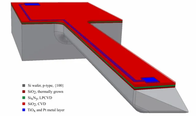
Figure 2.1. Simplified and non-proportional 3D model of the silicon probe with one site (close to its tip), the corresponding lead and a contact pad. Note that thin film layers deposited on the bulk silicon are magnified to make them visible.
Figure 2.2. (A) Back side mask for the first anisotropic etching. (B) Frontside mask for making holes above the sites and contact pads. (C) Back side mask for the second anisotropic etching. (D) Frontside mask for defining Pt pattern.
Figure 2.3. The plan view of the probe pattern.
Figure 2.4. Schematic representation of the probe fabrication process flow given in a cross-section through an electrode site (not to scale). A, B, C and D indicate the end of the 4 major processing steps with (A) thin film depositions and contact formation on the frontside, (B) defining the probe thickness by the first anisotropic etch, (C) Probe shaping with the combination of an anisotropic and isotropic wet etch from the back side and (D) removal of protecting layers and frame structure.
Figure 2.5. Optical micrograph of a probe shaft with thickness and width of 80 µm and 280 µm, respectively. The square shaped Pt contacts have a side length of 30 µm and are contacted to 4 µm wide leads.
Figure 2.6. The schematic illustration of a chip with the probe and the supporting frame from frontside (a) and backside (b). The four sites and corresponding leads are only the illustrations of the 24 recording sites that can be found on the fabricated probes.
Figure 2.7. Scanning Electron Microscopic (SEM) pictures of the silicon probe. Upper part of the figure shows the probe tip and 3 out of 24 Pt recording sites. The enlarged yacht bow like tip is seen on the bottom figure. Note the rounded shape and smooth surface of the back side of the probe. The imaging was carried out in a LEO 1540 XB SEM equipped with field emission gun, Gemini lens system and in-lens detector.
DOI:10.15774/PPKE.ITK.2010.004
LIST OF FIGURES 9
Figure 2.8. Light microscopic picture of a wafer with 25 probes in holder frames. Note that wet etching is not always immaculately accomplished resulting in residuals around the probe shaft (third row in the first column from left). Based on visual inspection for defects (short and open circuits, etching and insulator defects) the fabrication yield was about 40%.
Figure 2.9. Packaging of the acute silicon probe. Inset on the right side of the upper picture shows micro grids before bonding.
Figure 2.10. Impedance was measured before the acute experiments at 1 kHz with sine wave current less than 500 nA. The figure shows impedance values of 24 sites of 3 probes. Their average impedance was 1067.36±99.91 kΩ.
Figure 2.11. Result of a soak test of a probe with 2 bad sites (Nr. 2 and Nr. 5). Impedance measurement was carried out at 3 (blue), 6 (yellow), 9 (cyan), 12 (purple) and 24 (orange) hours after the first measurement while the probe was kept in Ringer solution.
The initial average impedance increased by 6.21% in 24 hours.
Figure 2.12. Activation resulted in decreased impedance on each site. The average impedance of this probe dropped from 1195.12±113.1 to 659.04±59.47, which is 55.14%
of the initial value. Before activation (green), after activation (purple).
Figure 2.13. LFP recorded from the MC and CPu of rat nr. 1. The 24th channel is allocated for indicating the time of stimuli if it is given. LFP gain: EEG (1k).
Figure 2.14. Outstanding MUA was recorded from the MC and CPu of rat Nr. 1. Unit activities could be isolated from 8 channels.
Figure 2.15. Magnified view of LFPs and MUAs belong to channels with good quality SUAs. The vertical scale bar represents 2 values, one belongs to MUA (+32 µV) and the other to LFP (+300 µV). Gain: EEG (1 k), MUA (50 k).
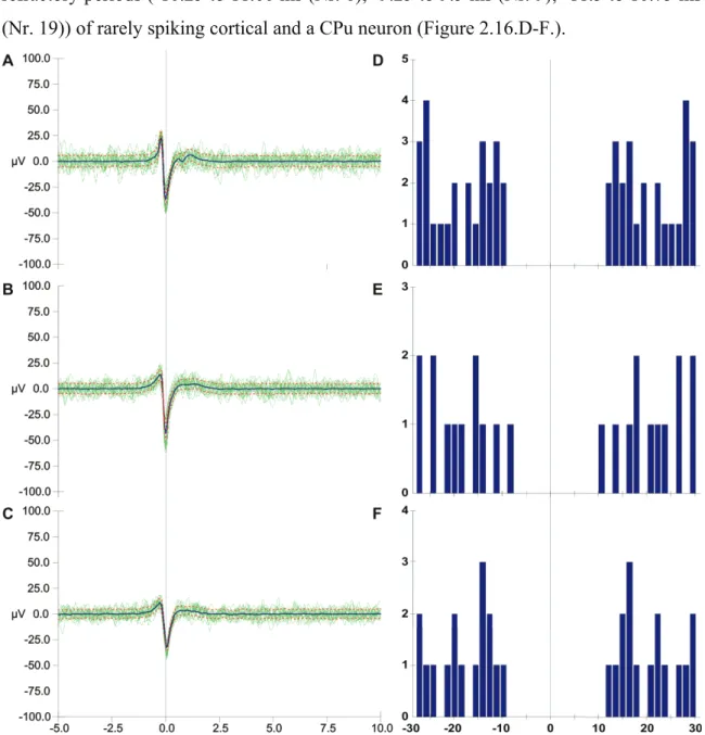
Figure 2.16. (A) 10 lowest and 10 highest amplitude spikes that belong to different neurons recorded on site Nr. 6 (A), Nr. 9 (B) and Nr. 19 (C) is depicted. Their averages (blue) and SDs (dotted orange lines) are presented. Auto-correlograms in the right column indicate refractory period of neuron recorded on site Nr. 6 (D), Nr. 9 (E) and Nr.
19 (F).
DOI:10.15774/PPKE.ITK.2010.004
LIST OF FIGURES
10
Figure 2.17. Good quality LFP and MUA characterized the recorded signal. Remarkable unit activity is seen in the signal that was acquired with the site located closest to tip (Nr.1). The vertical scale bar represents 2 values, one belongs to MUA (+32 µV) and the other to LFP (+300 µV) respectively. Gain: EEG (1k), MUA (50k).
Figure 2.18. A. 10 smallest and 10 highest amplitude firing activities of the same unit, the average of total 1249 spikes (orange) and their SD (dotted black line) are represented.
The recording site was located in the CPu. B. Histogram of the first channel unit shows no activity in the -1.6 ms and 1.6 ms range that means clearly distinguishable SUA was recorded on site Nr. 1. 60 bins with 0.5 ms resolution shows count numbers related to auto-correlogram.
Figure 3.1. Schematic drawing of implanted probe types (see details in [85]. Probes E100P had shanks with a cross section of 100 µm x 100 µm at the tip, 5 Pt electrode contacts on each shank, and a thin probe base for platform-based assembly (A). Probes D100C had shanks of 100 µm x 100 µm, no electrode contacts on the shafts, and a wider, 300 µm thick probe base for cable assembly (B). Probes D150C had shanks of 150 µm x 100 µm, no electrode contacts, and the wide probe base for cable assembly (C). A scanning electron micrograph shows a D100C probe in the silicon wafer (D). Sizes of the probes are indicated. Tracks of D100C and D150C probes are compared on light micrographs from the neuronal marker NeuN-stained sections (E).
Figure 3.2. Rat neocortex stained with the neuron marker NeuN (A) and the astroglial marker GFAP (B). The layers are indicated by dashed lines.
Figure 3.3. Effects of bleeding during implantation. Signs of serious bleeding during implantation were evident at both 1 week (A, B, arrows) and 12 weeks (C). The tissue was damaged around the probe tracks: a dark unspecific staining masked neuronal (A) and glial (B) immunostaining (DexM coated probe). In some cases, patches with severe neuron loss (asterisk) were observed near damaged tissue (C, Si probe) or next to the probe track without the signs of tissue damage (D, Dex coated probe).
DOI:10.15774/PPKE.ITK.2010.004
LIST OF FIGURES 11
Figure 3.4. Blood vessel distribution in rat neocortex. Photos (A, B) and drawings (C, D) show the cross section area of blood vessels in supragranular (A, C) and infragranular (B, D) layers of the cortex. Both small and large size blood vessels are more abundant in the supragranular layers (E); the average size (F) and the total area covered by the vessels (G) are also larger.
Figure 3.5. Effect of coating on neuronal densities. Light micrographs show similar neuron numbers around tracks made by probes with different coatings (A). The most serious neuron loss was observed at 1 week survival, in the vicinity of the track (<100 µm), neuron numbers ranging from 50% to 76% compared to control (B). The neuronal density increases with distance from the track, and with survival time, reaching 80% to 102% at 8 weeks (C). Different coatings affect neuronal survival at 1 week survival, but effects become less significant at longer intervals. The efficacy of the different coatings Hya<Dex<Si<Hya/DexM<DexM is similar for short or long term survival (D). Neuronal loss observed at short term decreases with survival time (E). Error bars represent mean±S.E.M. * p<0.001
Figure 3.6. Glial reaction around the probe tracks. In general, only moderate gliosis occurred at short (A, middle) and long (B, middle) term survival. Compared to control, larger and darkly stained reactive astroglial cells were visible around the tracks at 1 week survival (A, middle, right). At longer delays (12 weeks, B) glial cell numbers and shape returned to control levels (B, middle). In some cases, lower and higher glial reaction occurred around different shanks of the same probe (A, B), sometimes related to a serious bleeding (A, right).
Figure 3.7. Light micrographs show good preservation of neurons (A) and a slight gliosis (B) around native silicon probes after 1, 2, 4 and 12 weeks of survival.
Figure 3.8. Transmission electron micrographs of the probe tracks shown in Figure 3.6.
at 1 week (A, B) and 12 weeks (C, D) survival. Large caverns (asterisks) and damaged membranes were found next to the tracks at 1 week survival (A, B), whereas the tissue was not damaged at 12 weeks (C, D). In all cases, neuronal cell bodies (N on A, C, D) were found within 100 µm from the border of the probe tracks. Numerous neurons were observed at less than 20 µm from the track.
DOI:10.15774/PPKE.ITK.2010.004
LIST OF FIGURES
12
Figure 3.9. Transmission electron micrographs show the ultrastructure of the neural tissue 1 week after probe implantation. In case of no bleeding (A) signs of tissue damage were observed up to 30 µm from the track (arrows). When bleeding occurred (B) the tissue was damaged in a considerably higher radius (up to 130 µm in this case, arrows).
Figure 3.10. Transmission electron micrographs show synapses found close to the probe tracks at 1 week (A, B) and 12 weeks (C-F) survival. Membranes of the pre- and postsynaptic elements were discontinuous when the tissue was damaged around the probes (A, B), but the synaptic cleft seemed to be preserved (arrows). Numerous synapses were found in the close vicinity of the track, at both with low (C, D) and high (E, F) glial reaction. Squares on C and E are enlarged on D and F, respectively. Asterisk indicates part of the track.
Figure 3.11. Scanning electron micrographs of explanted probes. Low magnification photo shows the tissue residue partly covering the probe surface (A). Usually activated microglia-like, small round cells formed a densely packed layer on the explanted probes (B). Astroglia-like large (C), and small fusiform cells (D) were also observed. In some cases, electrode contacts were free of tissue residue (E), but totally covered contacts were also observed (F).
Figure 4.1. Auditory cortical fields on the temporal cortex of the cat [131]. (A) Lateral view. (B) Lateral view that is unfolded to show the part of the field that are normally hidden within the sulci (orange shading), as well as the high- and low-frequency limits of the tonotopic fields.
Figure 4.2. The thalamocortical loop. The CT cell sends excitatory synapses to TC and nRT cells. The CT cells excite CT and nRT cells. nRT neurons inhibit TC cells. TC:
thalamocortical, CT: corticothalamic; nRT: thalamic reticular cell [119].
Figure 4.3. Areas of the cat auditory cortex [164]
Figure 4.4. Shape and latencies of the main components of the auditory evoked potential (AEP) recorded from the median ectosylvian gyrus of an alert cat. The click stimulus was presented at 0 ms.
DOI:10.15774/PPKE.ITK.2010.004
LIST OF FIGURES 13
Figure 4.5. Cortical intracellular correlates of natural SWS, REM and waking states.
Parts indicated by arrows are expanded below (arrows). Note cyclic hyperpolarizations in SWS and diminished firing rate during ocular saccade in REM sleep [185].
Figure 4.6. Chronically implantable stainless steel laminar multielectrode with 24 Pt-Ir recording contacts.
Figure 4.7. A 5x5 guide tube matrix for chronic implantation.
Figure 4.8. Up- and down-state detection method based on linear filtering (B) and Hilbert transformation (C) of the recorded field potential (A).
Figure 4.9. LFP and unit responses to click stimuli in wakefulness and SWS. a, Continuous LFP traces in the wake state from representative depths of the AC covering superficial - top traces - and deep layers - bottom traces - respectively. b, Simultaneously recorded unit activity. Click stimulation is indicated by the trigger line below the unit traces. c, LFP traces in SWS. d, Unit traces in SWS. Translucent red marker strips indicate the time of AEPs in wake, while blue strips indicate the time evoked down- states. Note the large deep positive wave evoked by click stimulus only in SWS.
Figure 4.10. Click stimuli evoked LFP averages. The data was recorded from layer IV of the AC during SWS (blue), REM (red) and wakefulness (green). Click stimuli was given at 0 ms.
Figure 4.11. Averaged CSD, MUA and spectral responses time locked to click stimuli in wakefulness and SWS. a, CSD map of stimulus locked activity in wakefulness. Time: x- axis, stimulus is presented at 0 ms, cortical depth: y-axis. Sinks are depicted in red, sources in blue, arbitrary units. Laminarization is indicated by Roman numerals. b, Simultaneously recorded MUA map. Red indicates firing rate increase, blue decrease compared to baseline activity, arbitrary units. c, CSD map in SWS. d, Simultaneous MUA map in SWS. Note the large source and neuronal firing silence in SWS. e, LFP spectrogram (1-200Hz) from representative depths of the cortex in response to click stimuli in wakefulness. Each elongated rectangle represents different channel. Red indicates increased, blue decreased activity in arbitrary units compared to baseline. f, LFP spectrogram in response to the click in SWS. Grey rectangle shows the time frame of the down-state.
DOI:10.15774/PPKE.ITK.2010.004
LIST OF FIGURES
14
Figure 4.12. Time-frequency analyses (Morlet wavelet) of evoked activities (3/sec click) in SWS, REM and wakefulness. The timing of each stimulus is indicated with short black lines on time-axis. Intensive power increase is seen in every frequency band after the click stimuli in SWS, especially in the low frequency ranges. Note the long-lasting power decrease in SWS that is absent in REM or waking states. The wavelet maps were calculated using recordings derived from the same contact.
Figure 4.13. CSD and MUA maps of evoked and spontaneous down-states in SWS. a, Click evoked down-state (only if a down-state was detected within 15-35 ms interval post stimulus) onset locked CSD map. b, Stimulus evoked down-state onset locked MUA map. c, Spontaneously occurring down-state onset locked CSD map (the stimulus was switched off). d, Spontaneously occurring down-state onset locked MUA map. e, Difference CSD map of evoked and spontaneous down-states. Green indicates no significant differences (t-test, Bonferroni corrected to multiple comparison, p>0.2). f, Difference MUA map of evoked minus spontaneous down-states. Green indicates no significant differences (t-test, Bonferroni corrected to multiple comparison, p>0.2).
During the approximate time of the down-state (grey box) there are no significant differences between evoked and spontaneous activity.
Figure 4.14. MUA and CSD maps related to averages of down-states evoked with click stimuli in SWS and spontaneously occurring in KX anesthesia. Cortical layers are represented with roman numbers. Sinks on CSD maps are depicted with red, sources with blue, arbitrary unit. Red on MUA maps indicates increased, blue decreased activity in arbitrary units compared to baseline. Laminarization is indicated by Roman numerals.
Figure 4.15. CSD and MUA averages related to down-states evoked with click stimuli in SWS and spontaneously occurring in KX anesthesia.
DOI:10.15774/PPKE.ITK.2010.004
LIST OF FIGURES 15
Figure 4.16. CSD and MUA responses to double click stimuli in wakefulness and SWS.
a, CSD map in response to a short delay (40 ms) double click stimuli in wakefulness. b, CSD map in response to the short delay stimuli in SWS. c, CSD map in response to a long delay (80 ms) double click stimuli in wakefulness. d, CSD map in response to the long delay stimuli in SWS. Note that the CSD response to the second click on b, is highly suppressed and even the 80 ms delayed second stimulus on d can evoke a clear down-state. e, MUA (arbitrary units) from layer III of another cat time locked to the stimulus in wakefulness. Single click response in green, short (20 ms) delay double click response in red, long (100 ms) delay response in blue. f, MUA responses in SWS. Note the large difference at short delays (red trace) between wakefulness and SWS. Note also that the evoked down-state is present even in response to the 100 ms delayed second click in SWS.
DOI:10.15774/PPKE.ITK.2010.004
LIST OF TABLES
16
LIST OF TABLES
Table 2.I. Main steps of the probe fabrication process flow.
Table 2.II. Comparison of different properties of various probes Table 3.I. Implanted probe types and survival times.
Table 3.II. Percentage of neurons at certain distances from the probe track, compared to control, at short term (1 week) survivals. Data are presented in mean±S.E.M.
Table 3.III. Neuron numbers at certain distances from the probe track at 1 and 8 weeks survival. Data are given in mean±S.E.M.
Table 3.IV. Statistical significances for the different locations around the different probes, at 1 week survival.* p<0.05, ns= not significant
Table 3.V. Percentage of neurons at certain distances from the probe track, compared to control, at long term survivals (DexM>Hya/DexM>Si>Dex>Hya). Data are presented in mean±S.E.M.
Table 3.VI. Percentage of neurons at certain distances from the probe track, compared to control, at different time points, around E100P uncoated Si probes. Data are presented in mean±S.E.M.
DOI:10.15774/PPKE.ITK.2010.004
LIST OF ABBREVIATIONS 17
LIST OF ABBREVIATIONS
µ -WEMS: Micro-wire electrical discharge machining A: Anisotropy
AAF: Anterior auditory field
ABC: Avidin-biotinylated horseradish peroxidase complex AC: Auditory cortex
Ach: Acethylcholine
AEP: Auditory evoked potential AES: Anterior ectosylvian field AI: Primary auditory cortex AII: Secondary auditory cortex Al: Aluminum
AP: Anteroposterior BHF: Buffered HF BP filter: Band-pass filter CH3COOH: Acetic acid CSD: Current source density CT: Corticothalamic cells
CVD: Chemical vapor deposition
D100C: Dummy probe, 100 µm, Cable assembly D150C: Dummy probe, 150 µm, Cable assembly DAB: 3,3’-diaminobenzidine tetrahydrochloride dB: Decibel
Dex: Dextran
DexM: Dexamethasone
DRIE: Deep reactive ion etching DV: Dorsoventral
DWL: Direct write laser DZ: Dorsal auditory zone
E100P: Probe with electrodes, 100 µm, Platform assembly ED: Posterior ectosylvian gyrus
EEG: Electroencephalograph
DOI:10.15774/PPKE.ITK.2010.004
LIST OF ABBREVIATIONS
18
EI: Intermediate part of the posterior ectosylvian gyrus EMG: Electromyelography
EOG: Electrooculogram
EPSP: Excitatiry postsynaptic potential ERP: Event related potential
EV: Ventral part of the ectosylvian gyrus FFT: Fast Fourier transformation
fMRI: Functional magnetic resonance imaging FP: Field potential
GABA: γ-aminobutyric acid
GFAP: Glial fibrillary acidic protein H2N2: Hydrogen peroxide
H2SO4: Sulfuric acid H3PO4:Phosphoric acid Hc: Hippocampus HF: Hydrogen-fluoride HNO3: Nitric acid
Hya/DexM: Hyaluronic acid and Dexamethasone Hya: Hyaluronic acid
IC: Inferior colliculus In: Insular cortex
IPSP: Inhibitory postsynaptic potential IrOx: Iridium oxide
K+: Potassium
KOH: Potassum hydroxide KX: Ketamine-xylazine LFP: Local field potential
LPCVD: Low-pressure chemical vapor deposition MC: Motor cortex
MCFA: Multiple channel frequency analyzer ME: Multielectrode
MEMS: Micro-electro-mechanical systems MGB: Medial geniculate body
ML: Mediolateral
DOI:10.15774/PPKE.ITK.2010.004
LIST OF ABBREVIATIONS 19
MMN: Mismatch negativity MUA: Multiple unit activity
N1: Surface negative late component of the AEP NaOCl: Sodium hypochlorite
NaOH: Sodium hydroxide NeuN: Neuronal marker
nRT: Thalamic reticular nucleus OsO4: Osmium tetroxide
P: Posterior auditory cortex
P1: The first surface positive depth negative component of AEP P2: The second surface positive component of AEP
PAF: Posterior auditory field PB: Phosphate buffer
PCB: Printed circuit board PS: Paradoxical sleep
PSTH: Peri/Post-stimulus time histogram Pt: Platinum
REM: Rapid eye movement RF: Receptive field
RIE: Reactive ion etching
S.E.M.: Standard error of the mean SD: Standard deviation
SEM: Scanning electron microscopy Si: Silicon
SiNx ; SixNy:: Silicon nitride SiO2: Silicon dioxide SiOx: Silicon oxide SO: Slow oscillation SOI: Silicon-on-insulator SPL: Sound pressure level SPW-R: Sharp wave ripple SUA: Single unit activity SWS: Slow wave sleep TB: Tris buffer
DOI:10.15774/PPKE.ITK.2010.004
LIST OF ABBREVIATIONS
20
TC: Thalamocortical cell Te: Temporal cortex
TEM: Transmission electron microscopy Ti: Titanium
TiOx: Titanium oxide
TMAH: Tetramethylammonium hydroxide Ve: Ventral auditory area
VP: Ventral posterior auditory area
DOI:10.15774/PPKE.ITK.2010.004
Preface 21 C h a p t e r O n e
INTRODUCTION
1. Preface
When I started working in the Comparative Psychophysiology group at the Institute for Psychology of the Hungarian Academy of Sciences (IP-HAS) as an undergraduate student I always felt that air was full with mysticism because electrophysiology is a kind of science which medical aspects are barely understandable for an engineer. It was obvious for me from the very first moment that the first project I joined to and which related to development of various signal processing methods for neural signal analysis is only the entrance ticket to the wonderful and manifold world of electrophysiology.
Various cutting edge neural probes implantation and recording techniques and emerging biocompatibility issues thus material science and pharmacology related questions, as well as trying to find the answer to the question how a specific neural loop works with abstract thinking after measuring the local neural activities, were and still are compelling to me.
During the one-year lasting fellowship of the Hungarian American Enterprise Scholarship Fund (HAESF) at the middle of oldest beating heart of silicon based neural interface technology, the Neural Engineering Laboratory of the University of Michigan and the NeuroNexus Technologies Inc., I understood the limits of at that time the cutting- edge neural interfaces and emerging issues of their application. After my returning to Hungary I started to work on a novel extracellular multisite silicon probe at the Research Institute for Technical Physics and Materials Science of the Hungarian Academy of Sciences, with keeping in view the limits of Michigan probes. After reviewing the cutting edge neural interface technologies in the second chapter of my dissertation, I present the fabrication technology, packaging process and in vivo characterization of a novel multisite silicon probe. At the end of chapter two, discussion of difficulties and my future plans in connection with probe development are presented.
Emerging short and long-term biocompatibility issues draw the line for long-term applications of neural prosthesis. Within the frame of the NeuroProbes project I had the possibility to investigate what kinds of coating can reduce inflammatory responses around implanted inactive multishank silicon probes on short and long-terms. After a
DOI:10.15774/PPKE.ITK.2010.004
INTRODUCTION
22
brief introduction to different pharmacological agents currently used in neural interface technology to suppress immunological response in chapter three, my research methods and results on this project are presented with discussion and conclusion.
Multichannel neural probes are vital tools to advance understanding of cellular and system level functions in the central nervous system. To prove it, in chapter four I present the results of an experiment in which a chronically implantable multisite probe played a key role. Since the electrodes spanned the whole depth of the cortex and neural activities of cortical layers could be recorded from freely moving cats, I revealed how information processing changes in different states of the natural sleep-wake cycle as well as in ketamine-xylayine (KX) anesthesia. These results are put into the context of others’
findings in the discussion section.
In chapter five my main findings and novel scientific results are summarized. The author’s publication list and bibliography is presented at the end of this dissertation.
DOI:10.15774/PPKE.ITK.2010.004
Introduction 23 C h a p t e r T w o
A NOVEL MULTISITE SILICON PROBE FOR HIGH QUALITY LAMINAR NEURAL RECORDINGS
1. Introduction
Different approaches have been reported about various multisite probes or arrays.
Stereotrodes [6], tetrodes [7, 8] and micro-wire bundles [9, 10] were used first to record neural signals with many sites in acute and in chronic experiments. These technologies are still in use for ensemble recording. Their limitations, such as imprecise implantation, low recording resolution and low reproducibility are also well known [11]. Another big step towards the high spatial resolution recording was made by the introduction of wire based laminar microelectrode arrays. The micro-wire based thumbtack probe [12, 13] is a good example for that because it contains up to 24 contacts on one polyimide shank and its site spacing is precisely reproducible. A similar laminar array with a stainless steel shank is also known and used in experimental neuroscience [14, 15] as it is presented in chapter three. Another microwire based array approach was published by Nicolelis et al.
in 2003 [16]. Their fine wires are placed and fixed close to each other that yield high resolution data in long-term recordings. These measurements however, are limited to a cortical layer only since each wire, which cut end gives a recording contact, has the same length.
In contrast to the previously mentioned recording techniques, the silicon based multisite structures are not only precise and suitable for batch fabrication and have reproducible, small dimensions, but numerous contacts can be placed at different points along each probe. Moreover, they offer the potential of integrated signal processing circuits on them and the applied silicon dioxide and silicon nitride thin films have good biocompatible properties [17].
The first photoengraved brain microelectrode fabrication process based on wet etching was published early by Wise et al. [18]. This technology was further developed in order to fabricate fork-like shapes by using a combination of high temperature boron diffusion and wet etching [19]. However, the slow boron diffusion limits the maximum probe thickness to about 15µm that results in a fragile but less invasive probe with maximum
DOI:10.15774/PPKE.ITK.2010.004
A NOVEL MULTISITE SILICON PROBE FOR HIGH QUALITY LAMINAR NEURAL RECORDINGS
24
length of around 10 mm. Its modified version with on-chip integrated circuit [20] and 3D array configuration have also been developed [21-23].
Since the 1970s a wide variety of probes have been constructed by using different silicon fabrication methods. Besides the Michigan probes [18-24] the Utah array [25]
also became well known. It consists of 10×10 isolated silicon needles with tips exposed for potential recording. Since only a single tip-electrode is available per shaft, laminar recording from the cortex with this array is not feasible. An interesting micro-wire electrical discharge machining (µ-WEMS) based MEMS method for producing arrays has been developed recently by Rakwal et al. [26].
Plasma etching was also applied to define desired probe outlines rather than anisotropic wet etching [27-29]. Double-sided Deep Reactive Ion Etching (DRIE) processes were developed by different groups in order to produce probes with silicon-on- insulator (SOI) technology [30, 31]. A Direct Write Laser (DWL) based method was introduced by Kindlundh et al. [32] to realize fast custom design probe fabrication. The combination of Reactive Ion Etching (RIE) and DRIE methods was applied by the NeuroProbes consortium [33, 34] to form the desired probe thickness and shape. Within the frame of that project, various single shank, four shank [35], drug delivery [36], chemical sensor probes [37] and 3D arrays [38, 39] have been fabricated for acute and chronic use. Alternatives to silicon such as polyimide [11, 40, 41], parylene [42], glass [43] or thin film ceramic [44, 45] as possible probe substrates have also been investigated.
I present a novel wet chemical etching based process [46] that yields a highly reproducible silicon multi-electrode device that was fabricated at the Institute for Technical Physics and Materials Science of the Hungarian Academy of Sciences. This sensor contains 24 platinum recording contacts. The rounded probe with sharp and yacht- bow like tip provides high resolution, good quality recording. The maximum length and thickness of such a probe can be varied in a large scale. The body of the probe can easily be cleaned and reused because of its mechanical properties. The multichannel probe presented here could easily penetrate the dura and pia mater without bending, breaking or causing serious bleeding.
DOI:10.15774/PPKE.ITK.2010.004
Design 25
2. Design
2.1. Probe design
Each probe contains a single shaft, which can be inserted into the brain tissue, supported by a more robust connector part. Both the shaft and the connector part were made of the same single crystal silicon wafer, with bulk micromachining. On the surface of the connector part bonding pads have been placed, while on the 7 mm long, 280 µm wide and 80 µm thick shaft 24 square-shaped (30 µm × 30 µm) sites have been located for extracellular potential recording. The center-to-center distances of the neighbouring sites were chosen to be 100 µm, and the distance between the tip and the middle of the first contact window is 660 µm. The length of the tip is basically defined by the fabrication process, since yacht bow like and sharp tip was an elementary requirement from the very first stage of the design. The tip angle is approximately 26 degrees. Each site has been electronically connected to a bonding pad with 4 µm wide and 4 µm spaced wiring. The sites, the wires and the pads have been made of the same, 300 nm thick TiOx
and Pt layers. Figure 2.1. shows a simplified and non-proportional 3D model of the probe with one site, the corresponding lead and a contact pad.
Figure 2.1. Simplified and non-proportional 3D model of the silicon probe with one site (close to its tip), the corresponding lead and a contact pad. Note that thin film layers deposited on the bulk silicon are
magnified to make them visible.
DOI:10.15774/PPKE.ITK.2010.004
A NOVEL MULTISITE SILICON PROBE FOR HIGH QUALITY LAMINAR NEURAL RECORDINGS
26
A series of masks have been designed on the basis of the calculation considering the size effect of the silicon bulk etching processes. 4 masks (Figure 2.2.) are needed to form the 3 dimensional geometry as well as the electrodes, corresponding leads and contact pads on the microprobes. I designed these 4 masks with the Mask Edit software in 5x magnification compared to the real dimensions of the desired neural microprobes. The master masks corresponding to different photolithographic steps included the magnified version of a chip. The mask pattern was made out of 0.1 µm thin chrome layer on glass.
The pattern is then covered with 0.5 µm thin positive photoresist. The pattern is selectively developed by exposing the mask with light at 354 nm wavelength. I had to take into consideration that the maximum size of the diaphragm, which is used to flash the photoresist, is 3000 x 3000 µm in open position. The mask resolution is limited by the precise positioning abilities of the desk underneath the diaphragm. This is 1µm in x and y dimensions. The masks were manufactured at the MTA MFA.
The masks, which have been used in the fabrication process can be sorted into two categories: back side and frontside masks (Figure 2.2.). The two back side masks define the 3D structure of the probes. They have been designed on the basis of the calculation considering the size effect of the silicon bulk etching processes. The two frontside masks specify the patterns of the platinum and insulator layers.
Figure 2.2. (A) Back side mask for the first anisotropic etching. (B) Frontside mask for making holes above the sites and contact pads. (C) Back side mask for the second anisotropic etching. (D) Frontside
mask for defining Pt pattern.
DOI:10.15774/PPKE.ITK.2010.004
Design 27
Key features in the fabrication process include a sequence of wet etching processes to shape the probes from the back side. CVD silicon dioxide films and low stress LPCVD silicon nitride films are applied for insulating and protecting layers and one metal layer is deposited for the formation of electrodes, output leads and bonding pads. The plan view of the probe pattern is shown on Figure 2.3. A patent application that describes our method in details was submitted [46].
Figure 2.3. The plan view of the probe pattern.
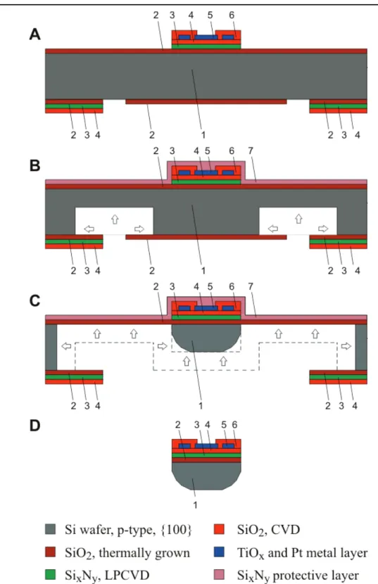
2.2. Fabrication process
Standard <100> oriented, p-type silicon wafer with a diameter of 3 inches and thickness of 200 µm polished on both sides were used for the probe fabrication (denoted by 1 on Figure 2.4.), that proceeded in 4 steps (Figure 2.4.). In initial thin-film deposition steps the bottom insulating layers (2,3,4), the electrodes and output leads (5), the passivation layer (6) are formed and the contact holes and bonding pads are opened (Figure 2.4.A.). The subsequent 2 steps consisted of different types of wet chemical etching processes for the probe shaping in order to obtain sharp tip with rounded edges (Figure 2.4.B-C.). The final phase of the probe fabrication process consisted of the removal of the protecting and masking layers and packaging of the probe (Figure 2.4.D.).
Residual stress in the passivation layers (i.e. bending) or other mechanical stress had no visible signs on the probe. The process flow is presented on Figure 2.4. and its summary is shown on Table 2.I.
DOI:10.15774/PPKE.ITK.2010.004
A NOVEL MULTISITE SILICON PROBE FOR HIGH QUALITY LAMINAR NEURAL RECORDINGS
28
Figure 2.4. Schematic representation of the probe fabrication process flow given in a cross-section through an electrode site (not to scale). A, B, C and D indicate the end of the 4 major processing steps with
(A) thin film depositions and contact formation on the frontside, (B) defining the probe thickness by the first anisotropic etch, (C) Probe shaping with the combination of an anisotropic and isotropic wet etch
from the back side and (D) removal of protecting layers and frame structure.
DOI:10.15774/PPKE.ITK.2010.004
Design 29 TABLE 2.I. MAIN STEPS OF THE PROBE FABRICATION PROCESS FLOW.
DOI:10.15774/PPKE.ITK.2010.004
A NOVEL MULTISITE SILICON PROBE FOR HIGH QUALITY LAMINAR NEURAL RECORDINGS
30
2.3. Contact formation
Silicon wafers were oxidized in steam atmosphere at 1150°C for 140 minutes in order to grow 900 nm thick SiO2 layers on both sides of the substrate. The thick oxide layer was removed from the frontside in buffered HF (BHF) while the back side was protected by photoresist (Microposit 1818). After that 100 nm thick SiO2 layer was grown using dry thermal oxidation at 1100°C for 40 minutes. Thermally grown SiO2 layers are denoted by 2 on Figure 2.4.A-D. 500 nm thick low stress (190 MPa) silicon nitride film was deposited by LPCVD at 830°C followed by a 200 nm thick CVD oxide deposition at 430°C, denoted by 3 and 4, respectively.
The metal layer (denoted by 5) was then deposited and patterned by lift-off process. In the photolithographic steps the axis of the mask pattern of the probe were aligned along the <100> and <010> crystallographic directions on both sides of the wafer. The lift-off structure composed of 1.8 µm thick photoresist (Microposit 1818) layer over patterned Al thin film of 500 nm. Al etching was performed in a 4 component etching solution, consisted of H2O, CH3COOH, H2SO4, H3PO4, and HNO3 in a ratio of 70:20:30:32:20, respectively. The metal layer consisted of a 15 nm thick adhesion layer of TiOx and Pt.
TiOx was formed by reactive sputtering of Ti in oxygen (Ar/O2 ratio was 80:20) atmosphere. In the same vacuum cycle 270 nm thick Pt was sputtered on top of TiOx.
The lift-off process was optimized by using water-cooled substrate holder which diminished the resist distortion during TiOx/Pt sputtering. It was followed by dissolving the photoresist pattern in acetone.
Subsequently, the removal of Al patterns in 4 component etching solution and chemical vapor deposition of SiO2 insulating layer (denoted by 6) of 1 µm thickness occurred. Contact holes through the CVD SiO2 were created by selective wet etching process. By these processing steps, Pt lines insulated by SiO2 layer and formation of Pt contacts have been carried out (Figure 2.5.).
DOI:10.15774/PPKE.ITK.2010.004
Design 31
Figure 2.5. Optical micrograph of a probe shaft with thickness and width of 80 µm and 280 µm, respectively. The square shaped Pt contacts have a side length of 30 µm and are contacted to 4 µm wide
leads.
In the next steps back side masking patterns were formed by photolithography and wet etching. The first back side lithography defines the supporting frame structure, followed by oxide wet etch in BHF from all the unmasked area. The second back side lithographic step defines the initial shape of the probe and protects the supporting frame, too. Figure 2.6. shows the schematic illustration of a chip with the probe and the supporting frame from frontside (a) and backside (b).
In the following process step SiNx is selectively etched from the front and back sides of the wafer in hot phosphoric acid.
A 500 nm thick low stress LPCVD (190MPa) SiNx layer was deposited on the frontside (denoted by 7) in order to use it as a protective coating during the following wet etching on the back side. Insulating and protecting SiNx and CVD SiO2 layers were deposited in 2 steps to avoid soaking via pin holes.
DOI:10.15774/PPKE.ITK.2010.004
A NOVEL MULTISITE SILICON PROBE FOR HIGH QUALITY LAMINAR NEURAL RECORDINGS
32
Figure 2.6. The schematic illustration of a chip with the probe and the supporting frame from frontside (a) and backside (b). The four sites and corresponding leads are only the illustrations of the 24 recording sites
that can be found on the fabricated probes.
2.4. Probe shaping
Steps #19-22 in Table 2.I., give an overview about the probe shaping as well as Figure 2.4.B-C. On the schematic cross section of Figure 2.4.B. the body of the probe was formed by using back side wet chemical etching in 3 steps. Each probe was connected to a larger Si frame, which made the handling of the probes easier. The frame was protected against corrosion during the etching processes.
On Figure 2.4. and Figure 2.6. the frame is shown on the left- and right-hand sides.
900 nm SiO2, 500 nm SixNy and 500 nm CVD SiOx multilayer stacks were used as a masking structure to protect the probe-holding frame (layer 2, 3, 4 on the back side) and the thicker area below the bonding pads, while a 900 nm SiO2 layer was used in the formation of the body and tip of the probe (layer 2 on the back side).
The anisotropic etching process was performed in 2 steps. The thickness of the probe was determined by the first step, where the side walls with <100> and <010> orientation had been developed, except on the probe tip where the side walls had different orientations. In the next step the SiO2 masking layer was removed from the back side of the probe, consequently, the top plane of the etched relief silicon pattern was exposed to the etching solution. The etching front propagated parallel to the etched planes having orientation of <100>, <010> and <001> until the whole thickness of silicon was removed between the probe bodies. The applied anisotropic etching solution contained a mixture of saturated sodium hypochlorite (NaOCl) and sodium hydroxide (NaOH) in aqueous
DOI:10.15774/PPKE.ITK.2010.004
Design 33
solution. This composition differed from the common alkaline etching baths (NaOH, KOH, TMAH) by the addition of a strong oxidizing agent. This etching solution provided a mirror-like, defect-free silicon surface, even after long etching periods.
Additionally, a reduction of the anisotropy (A) occurred, i.e. the ratio of the etch-rates (R<001>/R<111>) decreased. Anisotropy strongly depended on the NaOCl content of the solution. During the long anisotropic etching process, a reflux column was used in order to maintain the concentration level at 78°C. The applied novel type of anisotropic etching formed vertical walls, when the pattern alignment followed the <100> directions on the
<100> oriented wafer [47]. In summary, in the first step, around 100 µm of Si was removed, followed by the SiO2 mask dissolution by BHF. In the second step, the final formation i.e. the maskless etching of the needle was carried out, while the chip frame was protected by SiNx.
The sharp edges of the probe were removed by the next etching step that is isotropic polishing etching. A solution containing concentrated acids have been applied namely, HF and HNO3 for Si dissolution and H3PO4 for the reduction of the etching rate to 7- 8µm/min. An additive (non-ionic wetting agent) was also mixed with the etching solution. The volume ratio of HF and HNO3 has been chosen to 1:4 in order to have a forced etching rate at the edges of the samples. By using this etching step around 15 µm was removed from each side walls of the probe body. The combination of these different etching methods resulted in a probe shaft having rounded edges and yacht-bow-like sharp tip (Figure 2.7.).
DOI:10.15774/PPKE.ITK.2010.004
A NOVEL MULTISITE SILICON PROBE FOR HIGH QUALITY LAMINAR NEURAL RECORDINGS
34
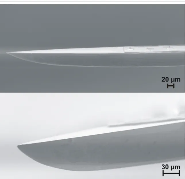
Figure 2.7. Scanning Electron Microscopic (SEM) pictures of the silicon probe. Upper part of the figure shows the probe tip and 3 out of 24 Pt recording sites. The enlarged yacht bow like tip is seen on the bottom figure. Note the rounded shape and smooth surface of the back side of the probe. The imaging was
carried out in a LEO 1540 XB SEM equipped with field emission gun, Gemini lens system and in-lens detector.
The residual stress of the passivation layers is so low that it could not bend the probes significantly. To measure the angle of the bending, shafts have been analyzed with optical microscope. The angle difference on the total length of the shaft (7200 µm) was less than 1 degree.
2.5. Packaging
After the removal of the SiO2 and SixNy protective layers, Pt contacts became uncovered and the probes could be flipped out of the holder frame (Figure 2.8.) one-by-
DOI:10.15774/PPKE.ITK.2010.004
Design 35
one. A special thinner connection was developed on the back side of the wafer in order to make the flipping out of the probe easier.
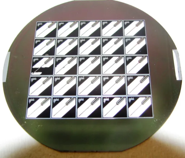
Figure 2.8. Light microscopic picture of a wafer with 25 probes in holder frames. Note that wet etching is not always immaculately accomplished resulting in residuals around the probe shaft (third row in the first column from left). Based on visual inspection for defects (short and open circuits, etching and insulator
defects) the fabrication yield was about 40%.
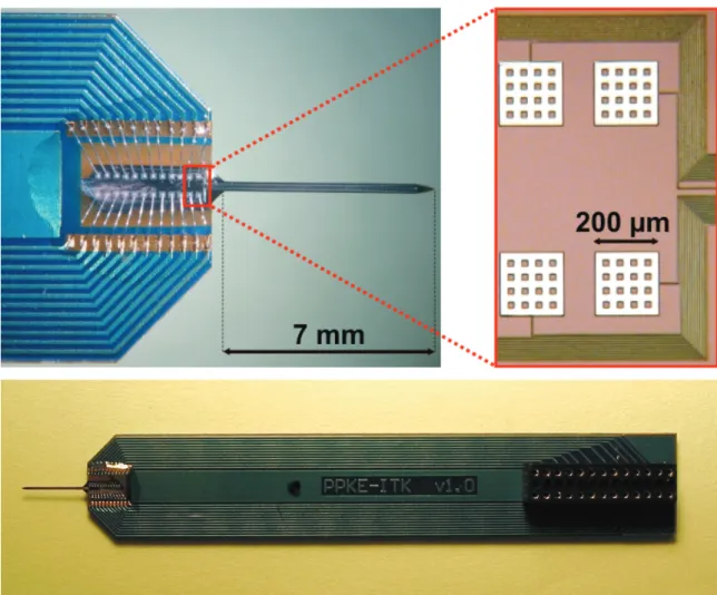
A Printed Circuit Board (PCB) specifically designed for this purpose was used for packaging (Figure 2.9.). The PCB I designed has a length and width of 6.8 cm and 1.2 cm, respectively. On one end of the PCB a 3x5 mm square is found that is not covered with lacquer. 24 gold contact pads are formed on longer sides of that square. The back of the silicon probe base had been glued to that square part of the PCB first with a 2 component epoxy resin (Araldit AY103/HY956). Connection between the silicon probe and the PCB was established via ultrasonic wire bonding (Kulicke-Soffa) using 50 µm thick Al wires. Since Al formed better bonding on SiO2 than on Pt, SiO2-Pt micro grids (200 µm x 200 µm) were designed to form the bonding pads (Figure 2.9. inset). After bonding, the vicinity of bonding area was covered by a drop of epoxy resin to protect it
DOI:10.15774/PPKE.ITK.2010.004
A NOVEL MULTISITE SILICON PROBE FOR HIGH QUALITY LAMINAR NEURAL RECORDINGS
36
from damaging. A 26 pole Preci-dip connector was soldered to the opposite end of the PCB but only 24 slots were functional.
Figure 2.9. Packaging of the acute silicon probe. Inset on the right side of the upper picture shows micro grids before bonding.
3. Results
3.1. Impedance measurement
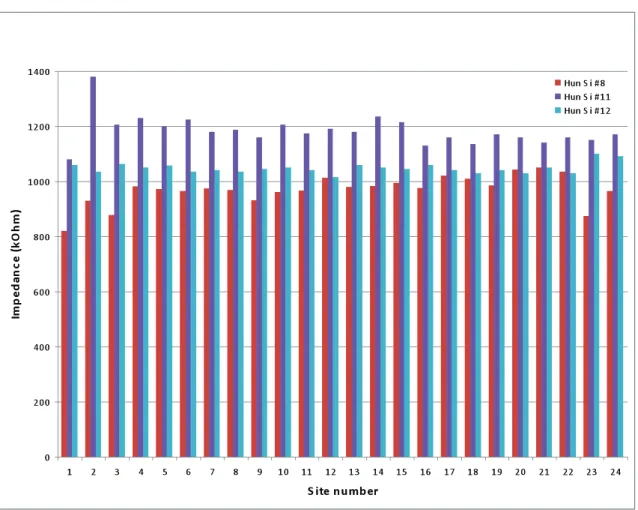
Before the acute animal experiments were conducted, impedance between each probe site and a counter platinum electrode had been measured in Ringer’s lactate solution (Teva Inc., Hungary). Every probe had been cleaned with absolute ethanol first then immersed into Ringer solution. An electroanalytical activation and sensing instrument (BAK model EASI-1, BAK Electronics) was used which measured the impedance at 1 kHz, with sine wave and current less than 500 nA. Average site impedance and standard deviation were calculated using data derived from 3 probes (Figure 2.10.). The average site impedance, calculated by taking into account of 3*24=72 sites, was 1067.36±99.91 kΩ that is consistent with previous results [39].
DOI:10.15774/PPKE.ITK.2010.004
Results 37
Figure 2.10. Impedance was measured before the acute experiments at 1 kHz with sine wave current less than 500 nA. The figure shows impedance values of 24 sites of 3 probes. Their average impedance was
1067.36±99.91 kΩ.
The upper SiO2 layer must perfectly insulate the extracellular space from leads otherwise the cross-talk between adjacent and even distant channels might increase, moreover shorts can develop. In case of shorts the impedance of participant sites and corresponding leads became similar and decrease significantly.
To investigate whether or not the upper passivation layer leaks I carried out a soak test. I immersed a probe with 2 bad sites into Ringer solution and left it in there for 24 hours. I measured the site impedances in every 3 of the first 12 hours, then 24 hours after the beginning of the experiment. No significant change was observed during the 24 hours timeframe (Figure 2.11.). Average at the beginning continuously increased from 1118.18±41.91 kΩ to 1204.27±65.66 kΩ (at 3 hours), 1248.68±33.91 kΩ (at 6 hours), 1231.86±32.88 kΩ (at 9 hours), 1206.046±44.94 kΩ (at 12 hours) to 1262±63.28 kΩ (at 24 hours). The initial average impedance increased by 6.21% in 24 hours. Given this fact using this probe for acute recording, that rarely takes longer than 12 hours, is safe.
DOI:10.15774/PPKE.ITK.2010.004
A NOVEL MULTISITE SILICON PROBE FOR HIGH QUALITY LAMINAR NEURAL RECORDINGS
38
Figure 2.11. Result of a soak test of a probe with 2 bad sites (Nr. 2 and Nr. 5). Impedance measurement was carried out at 3 (blue), 6 (yellow), 9 (cyan), 12 (purple) and 24 (orange) hours after the first measurement while the probe was kept in Ringer solution. The initial average impedance increased by
6.21% in 24 hours.
Decreasing the impedance of Pt is possible by a simple electrochemical etching method. This process makes the smooth surface of Pt sites coarse and therefore extending their overall surfaces. During this electrochemical etching Pt ions leave the metal layer subsequent upon an applied electric field [48]. I applied positive voltage (+ 2V) with the BAK EASI device through an electrode immersed into Saline and negative voltage (- 2V) through the probe for 10 seconds. The passing current did not exceed 30 µA. The average impedance of this probe dropped from 1195.12±113.1 kΩ to 659.04±59.47 kΩ, which is 55.14% of the initial value (Figure 2.12.). By repeating this process impedance could be reduced to the 300kΩ-400kΩ range. Impedances remained stable, i.e. no significant change was observed in 2-3 consecutive surgeries.
DOI:10.15774/PPKE.ITK.2010.004
Results 39
Figure 2.12. Activation resulted in decreased impedance on each site. The average impedance of this probe dropped from 1195.12±113.1 to 659.04±59.47, which is 55.14% of the initial value. Before
activation (green), after activation (purple).
3.2. Neural recordings
Wistar rats (200-300g) were used for the experiments. For initial anesthesia I administered a mixture of 37.5 mg/ml ketamine and 5 mg/ml xylazine at an injection volume of 0.2 ml/100 g body weight via intraperitoneal injections. Sleep-like state was maintained with consecutive updates of the same mixture (0.2 ml/hour). Animals (n=2) were mounted in a stereotaxic frame (David Kopf) and craniotomy was performed over the motor cortex (MC) (AP: [0.0 +3.0], ML: [1.0 +4.0], Reference point: Bregma). The PCB part of the probe was attached to a micromanipulator first, then the probe was inserted into the MC and down to the caudate-putamen (CPu, AP: +1.5 ML: +3.0) in 100 μm steps. Probes could easily penetrate the dura and pia mater without bending or breaking or causing serious bleeding. After recording from MC and CPu for 4 hours, the probe had been explanted, and the rat was sacrificed. All procedures were done according to Animal Care Regulations of IP HAS.
Wide bandwidth data (0.1 Hz - 7 kHz) with gain of 1000 was recorded with 20 kHz/channel sampling rate at 16bit precision (LabView, National Instruments) and stored
DOI:10.15774/PPKE.ITK.2010.004
A NOVEL MULTISITE SILICON PROBE FOR HIGH QUALITY LAMINAR NEURAL RECORDINGS
40
on hard drive. The low noise pre- and main-amplifiers, necessary for good quality signal recording, were custom designed and built in house [13].
Multichannel Local Field Potential (LFP, BP filter: 0.1Hz-500Hz, 24 dB/decade, zero phase shift) and Multiple Unit Activities (MUA, BP filter: 500Hz-5000Hz, 24dB/oct, zero phase shift) were separated offline from the recorded raw data via band-pass filtering. LFP and MUA data were analyzed with NeuroScan 4.3 software (Compumedics, El Paso, TX). Off-line analyses included zero phase shift filtering, thresholding, epoching, baselining and averaging of the signals.
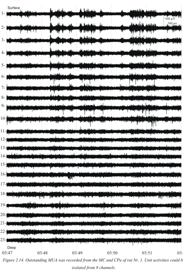
Good quality LFP (Figure 2.13) and MUA (Figure 2.14) was apparent on each channel recorded from rat Nr. 1. LFP was characterized by slow-wave components, a phenomenon typical for ketamine-xylazine (KX) anesthesia [49]. 8 sites located in MC and CPu recorded remarkable unit activities, high amplitude spikes well exceeded the background activity (Figure 2.14;Figure 2.15).
Figure 2.13. LFP recorded from the MC and CPu of rat nr. 1. The 24th channel is allocated for indicating the time of stimuli if it is given. LFP gain: EEG (1k).
DOI:10.15774/PPKE.ITK.2010.004
Results 41
Figure 2.14. Outstanding MUA was recorded from the MC and CPu of rat Nr. 1. Unit activities could be isolated from 8 channels.
Spikes with maximum amplitude higher than 3.5xSD had been detected first with the Spike 2 software [Cambridge Electronic Design, http://www.ced.co.uk/pru.shtml] then
DOI:10.15774/PPKE.ITK.2010.004
A NOVEL MULTISITE SILICON PROBE FOR HIGH QUALITY LAMINAR NEURAL RECORDINGS
42
sorted using the built in CEM sorter of DataView 4.7 demo and Klustawin [http://www.st-andrews.ac.uk/~wjh/klustawin/]. Single Unit Activity (SUA) on at least 6 channels had adequately high amplitude activity to be reliably separated from MUAs.
Sorted spikes on channel 6, 9 and 12 (n=500 on channel 6; n=438 on channel 9; n=215 on channel 19) are presented on Figure 2.16.A-C.
Figure 2.15. Magnified view of LFPs and MUAs belong to channels with good quality SUAs. The vertical scale bar represents 2 values, one belongs to MUA (+32 µV) and the other to LFP (+300 µV). Gain: EEG
(1 k), MUA (50 k).
DOI:10.15774/PPKE.ITK.2010.004
Results 43
On Figure 2.16.A-C. the 10 lowest and 10 highest amplitude spikes, that belong to 3 different neurons recorded on 3 sites (6, 9 and 19), are indicated. The average action potentials (blue) and standard deviations (SD, dotted orange lines) are also shown. The average amplitude of the spike peak is -37.60±4.95 µV (Nr. 6), -43.75±5.26 µV (Nr. 9) and -32.78±4.13 µV (Nr. 19). Auto-correlations (40 bins with 1.5 ms resolution) show refractory periods (-10.25 to 11.00 ms (Nr. 6); -9.25 to 9.5 ms (Nr. 9); -11.5 to 10.75 ms (Nr. 19)) of rarely spiking cortical and a CPu neuron (Figure 2.16.D-F.).
Figure 2.16. (A) 10 lowest and 10 highest amplitude spikes that belong to different neurons recorded on site Nr. 6 (A), Nr. 9 (B) and Nr. 19 (C) is depicted. Their averages (blue) and SDs (dotted orange lines) are presented. Auto-correlograms in the right column indicate refractory period of neuron recorded on site Nr.
6 (D), Nr. 9 (E) and Nr. 19 (F).
DOI:10.15774/PPKE.ITK.2010.004
A NOVEL MULTISITE SILICON PROBE FOR HIGH QUALITY LAMINAR NEURAL RECORDINGS
44
In the experiment with rat Nr. 2 another probe was used. In that case every contact recorded good quality LFPs and MUAs from the CPu. Recording site, located closest to the tip (Nr. 1), showed remarkable unit activity (Figure 2.17.) but SUAs on at least 2 channels had adequately high amplitude activity to separate. Other sites located more dorsal but still in CPu could also record clearly distinguishable population cellular firing (MUA) activity. LFP and MUA recorded from tip, middle and distal sites are shown on Figure 2.17.
Figure 2.17. Good quality LFP and MUA characterized the recorded signal. Remarkable unit activity is seen in the signal that was acquired with the site located closest to tip (Nr.1). The vertical scale bar represents 2 values, one belongs to MUA (+32 µV) and the other to LFP (+300 µV) respectively. Gain:
EEG (1k), MUA (50k).
Spikes (n=1249) with maximum amplitude higher than 3xSD = 25.5 µV had been detected. The average amplitude of the spike peak is -41.7±8.2 µV at 50 µs. Figure
DOI:10.15774/PPKE.ITK.2010.004