1
SECTION 5
HIGH SPEED ADC APPLICATIONS
Walt Kester, Brad Brannon, Paul Hendricks
D RIVING ADC I NPUTS FOR L OW D ISTORTION AND W IDE
D YNAMIC R ANGE
In order to achieve wide dynamic range in high speed ADC applications, careful attention must be given to the analog interface. Many ADCs are designed so that analog signals can be interfaced directly to their inputs without the necessity of a drive amplifier. This is especially true in ADCs such as the AD9220/21/23 family and the AD9042, where even a low distortion drive amplifier may result in some degradation in AC performance. If a buffer amplifier is required, it must be carefully selected so that its distortion and noise performance is better than that of the ADC.
Single-supply ADCs generally yield optimum AC performance when the common- mode input voltage is centered between the supply rails (although the optimum common-mode voltage may be skewed slightly in either direction about this point depending upon the particular design). This also eases the drive requirement on the input buffer amplifier (if required) since even "rail-to-rail" output op amps give best distortion performance if their output is centered about mid-supply, and the peak signals are kept at least 1V from either rail.
Typical high speed single-supply ADC peak-to-peak input voltage ranges may vary from about 0.5V to 5V, but in most cases, 1V to 2V peak-to-peak represents the optimum tradeoff between noise and distortion performance.
In single-supply applications requiring DC coupling, careful attention must be given to the input and output common-mode range of the driving amplifier. Level shifting is often required in order to center a ground-referenced signal within the allowable common-mode input range of the ADC.
Small RF transformers are quite useful in AC coupled applications, especially if the ADC has differential inputs. Significant improvement in even-order distortion products and common-mode noise rejection may be realized, depending upon the characteristics of the ADC.
An understanding of the input structure of the ADC is therefore necessary in order to properly design the analog interface circuitry. ADCs designed on CMOS processes typically connect the sample-and-hold switches directly to the analog input, thereby generating transient current pulses. These transients may significantly degrade performance if the settling time of the op amp is not sufficiently fast. On the other hand, ADCs designed on bipolar processes may present a relatively benign load to the drive amplifier with minimal transient currents.
The data sheet for the ADC is the prime source an engineer should use in designing the interface circuits. It should contain recommended interface circuits and spell out relevant tradeoffs. However, no data sheet can substitute for a fundamental
understanding of what's inside the ADC.
HIGH SPEED ADC INPUT CONSIDERATIONS
n
n Selection of Drive Amplifier (Only if Needed!) n
n Single Supply Implications n
n Input Range (Span): Typically 1V to 2V peak-to-peak for best distortion / noise tradeoff
n
n Input Common-Mode Range:
Vs / 2 (Nominally) for Single Supply ADCs n
n Differential vs. Single-Ended n
n AC Coupling Using Transformers n
n Input Transient Currents
a 5.1
Switched-Capacitor Input ADCs
The AD9220/21/23-series of ADCs are excellent examples of the progress that has been made in utilizing low-cost CMOS processes to achieve a high level of
performance. A functional block diagram is shown in Figure 5.2. This family of ADCs offers sampling rates of 1.25MSPS (AD9221), 3MSPS (AD9223), and 10MSPS (AD9220) at power dissipations of 60, 100, and 250mW respectively. Key
specifications for the family of ADCs are given in Figure 5.3. The devices contain an on-chip reference voltage which allows the full scale span to be set at 2V or 5V peak- to-peak (full scale spans between 2V and 5V can be set by adding two external gain setting resistors).
3
5.2 AD922X-SERIES ADC FUNCTIONAL DIAGRAM
a
VINA
CAPT CAPB
SENSE
OTR BIT 1 (MSB) BIT 12 (LSB) VREF
DVSS
AVSS CML
AD9221/23/20
SHA
DIGITAL CORRECTION LOGIC
OUTPUT BUFFERS VINB
1V
REFCOM 5 5
4 4
3
3 3
12
DVDD CLK AVDD
MODE SELECT
MDAC3 GAIN = 4 MDAC2
GAIN = 8 MDAC1
GAIN = 16
A/D A/D
A/D A/D
AD9220, AD9221, AD9223
CMOS 12-BIT ADCs KEY SPECIFICATIONS
n
n Family Members:
AD9221 (1.25MSPS), AD9223 (3MSPS), AD9220 (10MSPS) n
n Power Dissipation: 60, 100, 250mW, Respectively n
n FPBW: 25, 40, 60MHz, Respectively n
n Effective Input Noise: 0.1LSB rms (Span = 5V) n
n SINAD: 71dB n
n SFDR: 88dBc n
n On-Chip Reference n
n Differential Non-Linearity: 0.3LSB n
n Single +5V Supply n
n 28-Pin SOIC Package
a 5.3
The input circuit of the AD9220/21/23-series of CMOS ADCs contains the
differential sample-and-hold as shown in Figure 5.4. The switches are shown in the track mode. They open and close at the sampling frequency. The 16pF capacitors represent the effective capacitance of switches S1 and S2 plus the stray input capacitance. The Cs capacitors (4pF) are the sampling capacitors, and the CH capacitors are the hold capacitors. Although the input circuit is completely differential, the ADC can be driven either single-ended or differential. Optimum SFDR, however, is obtained using a differential transformer drive.
5.4 SIMPLIFIED INPUT CIRCUIT OF AD922X ADC FAMILY
VINB
a
+
-
SWITCHES SHOWN IN TRACK MODE A
VINA
CP 16pF
CP 16pF
S1
S2 S3
S4
S5
S7 S6
CS 4pF
CS 4pF
CH 4pF
CH 4pF
In the track mode, the differential input voltage is applied to the Cs capacitors.
When the circuit enters the hold mode, the voltage across the sampling capacitors is transferred to the CH hold capacitors and buffered by the amplifier A. (The switches are controlled by the appropriate phases of the sampling clock). When the SHA returns to the track mode, the input source must charge or discharge the voltage stored on Cs to the new input voltage. This action of charging and discharging Cs, averaged over a period of time and for a given sampling frequency fs, makes the input impedance appear to have a benign resistive component. However, if this action is analyzed within a sampling period (1/fs), the input impedance is dynamic, and hence certain precautions on the input drive source should be observed.
The resistive component to the input impedance can be computed by calculating the average charge that is drawn by CH from the input drive source. It can be shown that if Cs is allowed to fully charge to the input voltage before switches S1 and S2 are opened that the average current into the input is the same as if there were a
5
resistor equal to 1/(Csfs) connected between the inputs. Since Cs is only a few picofarads, this resistive component is typically greater than several kΩ for an fs = 10MSPS.
If one considers the SHA's input impedance over a sampling period, it appears as a dynamic load to the input drive source. When the SHA returns to the track mode, the input source should ideally provide the charging current through the Ron of switches S1 and S2 in an exponential manner. The requirement of exponential charging means that the source impedance should be both low and resistive up to and beyond the sampling frequency.
The output impedance of an op amp can be modeled as a series inductor and resistor. When a capacitive load is switched onto the output of the op amp, the output will momentarily change due to its effective high frequency output
impedance. As the output recovers, ringing may occur. To remedy this situation, a series resistor can be inserted between the op amp and the SHA input. The optimum value of this resistor is dependent on several factors including the sampling
frequency and the op amp selected, but in most applications, a 30 to 50Ω resistor is optimum.
The input voltage span of the AD922X-family is set by pin-strap options using the internal voltage reference (see Figure 5.5). The common-mode voltage can be set by either pin strap or applying the common-mode voltage to the VINB pin. Tradeoffs can be made between noise and distortion performance. Maximum input range allowable is 5V peak-to-peak, in which case, the common-mode input voltage must be one-half the supply voltage, or +2.5V. The minimum input range is 2V peak-to- peak, in which case the common-mode input voltage can be set from +1V to +4V. For best DC linearity and maximum signal-to-noise ratio, the ADC should be operated with an input signal of 5V peak-to-peak. However, for best high frequency noise and distortion performance, 2V peak-to-peak with a common-mode voltage of +2.5V is preferred. This is because the CMOS FET on-resistance is a minimum at this voltage, and the non-linearity caused by the signal-dependence of Ron (Ron modulation effect) is also minimal.
AD922X ADC INPUT VOLTAGE RANGE OPTIONS
SINGLE-ENDED INPUT Input Signal Range
(Volts)
Peak-to-Peak Signal (Volts)
Common-Mode Voltage (Volts)
0 to +2 2 +1
0 to +5 5 +2.5
+1.5 to +3.5 2 +2.5
DIFFERENTIAL INPUT
Input Signal Range Peak-to-Peak Signal Common-Mode Voltage
(Volts) Differential (Volts) (Volts)
+2 to +3 2 +2.5
+1.25 to +3.75 5 +2.5
a 5.5
Figure 5.6 shows the THD performance of the AD9220 for a 2V peak-to-peak input signal span and common-mode input voltage of 2.5V and 1V. The data was taken with a single-ended drive. Note that the performance is significantly better for Vcm
= +2.5V.
a
AD9220 THD VS. INPUT FREQUENCY: SINGLE-ENDED DRIVE 2V p-p INPUT, Vcm = +1V AND Vcm = +2.5V, fs = 10MSPS
5.6
THD (dBc)
INPUT FREQUENCY (MHz) Vcm = +1V
Vcm = +2.5V
50
60
70
80
90
0.1 0.2 0.5 1 2 5 10
A simple single-ended circuit for AC coupling into the inputs of the AD9220-family is shown in Figure 5.7. Note that the common-mode input voltage is set for +2.5V by the 4.99kΩ resistors. The input impedance is also balanced for optimum distortion performance.
7
5.7 SINGLE-ENDED AC-COUPLED
DRIVE CIRCUIT FOR AD922X ADC
33ΩΩ
+5V
a
4.99kΩΩ
0.1µµF
33ΩΩ 4.99kΩΩ
4.99kΩΩ
4.99kΩΩ 10µµF
0.1µµF +5V 10µµF
51.1ΩΩ INPUT
+
+5V
AD922X VINA
VINB
+
+2.5V
If the input to the ADC is coming from a long coaxial cable run, it may be desirable to buffer the transient currents at the ADC inputs from the cable to prevent
problems resulting from reflections, especially if the cable is not source-terminated.
The circuit shown in Figure 5.8 uses the low distortion AD8011 op amp as a buffer which can optionally provide signal gain. In all cases, the feedback resistor should be fixed at 1kΩ for best op amp performance, since the AD8011 is a current-feedback type. In this type of arrangement, care must be taken to observe the allowable input and output range of the op amp. The AD8011 input common-mode range (operating on a single +5V supply) is from +1.5 to +3.5V, and its output +1V to +4V. The ADC should be operated with a 2V peak-to-peak input range. The 33Ω series resistor is required to isolate the output of the AD8011 from the effective input capacitance of the ADC. The value was empirically determined to yield the best high-frequency SINAD.
5.8 BUFFERED AC-COUPLED INPUT DRIVE
CIRCUIT FOR AD922X ADC
+5V
a
4.99kΩΩ
33ΩΩ 4.99kΩΩ
4.99kΩΩ 10µµF
0.1µµF +5V
10µµF
51.1ΩΩ INPUT
+
+5V
AD922X VINA
VINB
+
- AD8011
+5V
4.99kΩΩ
0.1µµF 1kΩΩ 0.1µµF
1kΩΩ
33ΩΩ
10µµF +
2Vp-p 1Vp-p
+2.5V
Direct coupling of ground-referenced signals using a single supply requires the use of an op amp with an acceptable common-mode input voltage, such as the AD8041 (input can go to 200mV below ground). The circuit shown in Figure 5.9 level shifts the ground-referenced bipolar input signal to a common-mode voltage of +2.5V at the ADC input. The common-mode bias voltage of +2.5V is developed directly from an AD780 reference, and the AD8041 common-mode voltage of +1.25V is derived with a simple divider.
9
5.9 DIRECT-COUPLED LEVEL SHIFTER
FOR DRIVING AD922X ADC INPUT
a
10µµF +5V
52.3ΩΩ INPUT
+
+5V
AD922X VINA
VINB
+ - AD8041
+5V
0.1µµF 1kΩΩ
0.1µµF 1kΩΩ
33ΩΩ
AD780 2.5V REF.
1kΩΩ
±1V
+1.25V
+2.5V 1kΩΩ
10µµF
33ΩΩ +
+2.5V 1V±
Transformer coupling provides the best CMR and the lowest distortion. Figure 5.10 shows the suggested circuit. The transformer is a Mini-Circuits RF transformer, model #T4-6T which has an impedance ratio of four (turns ratio of 2). The schematic assumes that the signal source has a 50Ω source impedance. The 1:4 impedance ratio requires the 200Ω secondary termination for optimum power transfer and VSWR. The Mini-Circuits T4-6T has a 1dB bandwidth from 100kHz to 100MHz. The center tap of the transformer provides a convenient means of level shifting the input signal to the optimum common-mode voltage. The AD922X CML pin is used to provide the +2.5 common-mode voltage.
5.10 TRANSFORMER COUPLING INTO AD922X ADC
a
+5V
AD922X VINA
VINB
0.1µµF
+2.5V 33ΩΩ
CML
33ΩΩ
200ΩΩ 1:2
RF TRANSFORMER:
MINI-CIRCUITS T4-6T
2Vp-p 49.9ΩΩ
Transformers with other turns ratios may also be selected to optimize the performance for a given application. For example, a given input signal source or amplifier may realize an improvement in distortion performance at reduced output power levels and signal swings. Hence, selecting a transformer with a higher
impedance ratio (i.e. Mini-Circuits #T16-6T with a 1:16 impedance ratio, turns ratio 1:4) effectively "steps up" the signal level thus reducing the driving requirements of the signal source.
Note the 33Ω series resistors inserted between the transformer secondary and the ADC input. These values were specifically selected to optimize both the SFDR and the SNR performance of the ADC. They also provide isolation from transients at the ADC inputs. Transients currents are approximately equal on the VINA and VINB inputs, so they are isolated from the primary winding of the transformer by the transformer's common-mode rejection.
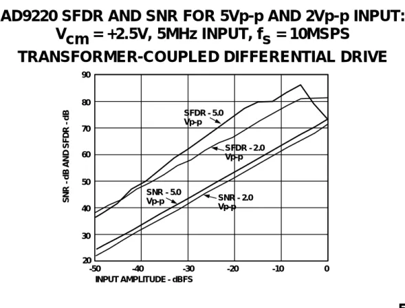
Transformer coupling using a common-mode voltage of +2.5V provides the maximum SFDR when driving the AD922X-series. By driving the ADC
differentially, even-order harmonics are reduced compared with the single-ended circuit. Figure 5.11 shows a plot of SFDR and SNR for the transformer-coupled differential drive circuit using 2V p-p and 5V p-p inputs and a common-mode voltage of +2.5V. Note that the SFDR is greater than 80dBc for input signals up to full scale with a 5MHz input signal.
11
5.11 AD9220 SFDR AND SNR FOR 5Vp-p AND 2Vp-p INPUT:
Vcm = +2.5V, 5MHz INPUT, fs = 10MSPS
TRANSFORMER-COUPLED DIFFERENTIAL DRIVE
a
INPUT AMPLITUDE - dBFS 90
50
20
-50 -40 -30 -20 -10 0
80
70
40
30 60
SNR - 5.0 Vp-p
SFDR - 5.0 Vp-p
SFDR - 2.0 Vp-p
SNR - 2.0 Vp-p
SNR - dB AND SFDR - dB
Figure 5.11 also shows differences between the SFDR and SNR performance for 2V p-p and 5V p-p inputs. Note that the SNR with a 5V p-p input is approximately 2dB to 3dB better than that for a 2V p-p input because of the additional dynamic range provided by the larger input range. Also, the SFDR performance using a 5V p-p input is 3 to 5dB better for signals between about –6dBFS and –36dBFS. This improvement in SNR and SFDR for the 5V p-p input range may be advantageous in systems which require more than 6dB headroom to minimize clipping of the ADC.
Driving Bipolar Input ADCs
Bipolar technology is typically used for extremely high performance ADCs with wide dynamic range and high sampling rates such as the AD9042. The AD9042 is a state- of-the-art 12-bit, 41MSPS two stage subranging ADC consisting of a 6-bit coarse ADC and a 7-bit residue ADC with one bit of overlap to correct for any DNL, INL, gain or offset errors of the coarse ADC, and offset errors in the residue path. A block diagram is shown in Figure 5.12 and key specifications in Figure 5.13. A proprietary gray-code architecture is used to implement the two internal ADCs. The gain
alignments of the coarse and residue, likewise the subtraction DAC, rely on the statistical matching of the devices on the process. As a result, 12-bit integral and differential linearity is obtained without laser trim. The internal DAC consists of 126 interdigitated current sources. Also on the DAC reference, there are an
additional 20 interdigitated current sources to set the coarse gain, residue gain, and full scale gain. The interdigitization removes the requirement for laser trim. The AD9042 is fabricated on a high speed dielectrically isolated complementary bipolar process. The total power dissipation is only 575mW when operating on a single +5V supply.
a
AD9042 12-BIT, 41MSPS ADC BLOCK DIAGRAM
5.12
+ - ANALOG
INPUT
7
12
ERROR CORRECTION LOGIC
OUTPUT REGISTERS SHA
1
SHA 2
6-BIT ADC
6-BIT DAC
7-BIT ADC SHA
3 GAIN
12 BUFFER
REGISTER 6
6
AD9042 12-BIT, 41MSPS ADC KEY SPECIFICATIONS
n
n Input Range: 1V peak-to-peak, Vcm = +2.4V n
n Input Impedance: 250ΩΩ to Vcm n
n Effective Input Noise: 0.33LSBs rms n
n SFDR at 20MHz Input: 80dB n
n SINAD at 20MHz Input = 66dB n
n Digital Outputs: TTL Compatible n
n Power Supply: Single +5V n
n Power Dissipation: 575mW n
n Fabricated on High Speed Dielectrically Isolated Complementary Bipolar Process
a 5.13
The outstanding performance of the AD9042 is partly due to the use of differential techniques throughout the device. The low distortion input amplifier converts the single-ended input signal into a differential one. If maximum SFDR performance is
13
desired, the signal source should be coupled directly into the input of the AD9042 without using a buffer amplifier. Figure 5.14 shows a method using capacitive coupling. Transformer coupling can also be used if desired.
5.14 INPUT STRUCTURE OF AD9042 ADC IS
DESIGNED TO BE DRIVEN DIRECTLY FROM 50 Ω Ω SOURCE FOR BEST SFDR
a
FROM 50ΩΩ SOURCE
RT 61.9ΩΩ
250ΩΩ
250ΩΩ
AD9042
INPUT = 1V p-p
+ -
The AD9050 is a 10-bit, 40MSPS single supply ADC designed for wide dynamic range applications such as ultrasound, instrumentation, digital communications, and professional video. Like the AD9042, it is fabricated on a high speed
complementary bipolar process. A block diagram of the AD9050 (Figure 5.15) illustrates the two-step subranging architecture, and key specifications are summarized in Figure 5.16.
a 5.15
AD9050 10-BIT, 40MSPS SINGLE SUPPLY ADC
ENCODE
AMP ARRAY
6-BIT ADC
DECODE LOGIC ERROR
CORRECTION DECODE
LOGIC AD9050
BANDGAP REFERENC
E
5-BIT ADC
10 AIN
AIN
VREFOUT
VREFIN REFBP
AD9050 10-BIT, 40MSPS ADC KEY SPECIFICATIONS
n
n 10-Bits, 40MSPS, Single +5V Supply n
n Selectable Digital Supply: +5V, or +3V n
n Low Power: 300mW on BiCMOS Process n
n On-Chip SHA and +2.5V reference n
n 56dB S/(N+D), 9 Effective Bits, with 10.3MHz Input Signal n
n No input transients, Input Impedance 5kΩΩ, 5pF n
n Input Range +3.3V ±0.5V Single-Ended or Differential n
n 28-pin SOIC / SSOP Packages n
n Ideal for Digital Beamforming Ultrasound Systems
a 5.16
The analog input circuit of the AD9050 (see Figure 5.17) is differential, but can be driven either single-endedly or differentially with equal performance. The input signal range of the AD9050 is ±0.5V centered around a common-mode voltage of
15
+3.3V, which makes single supply op amp selection more difficult since the amplifier has to drive +3.8V peak signals with low distortion.
5.17 AD9050 SIMPLIFIED INPUT CIRCUIT
GND
INPUT RANGE:
+3.3V ± 0.5V
INPUT BUFFER
+5V
AIN(A)
AIN(B)
8kΩΩ
16kΩΩ
8kΩΩ
16kΩΩ
a
The input circuit of the AD9050 is a relatively benign and constant 5kΩ in parallel with approximately 5pF. Because of its well-behaved input, the AD9050 can be driven directly from 50, 75, or 100Ω sources without the need for a low-distortion buffer amplifier. In ultrasound applications, it is normal to AC couple the signal (generally between 1MHz and 15MHz) into the AD9050 differential inputs using a wideband transformer as shown in Figure 5.18. The Mini-Circuits T1-1T
transformer has a 1dB bandwidth from 200kHz to 80MHz. Signal-to-noise plus distortion (SINAD) values of 57dB (9.2 ENOB) are typical for a 10MHz input signal.
If the input signal comes directly from a 50, 75, or 100Ω single-ended source, capacitive coupling as shown in Figure 5.18 can be used.
5.18 AC COUPLING INTO THE INPUT OF THE AD9050 ADC
TRANSFORMER COUPLING
16kΩΩ 16kΩΩ
50ΩΩ
CAPACITIVE COUPLING
8kΩΩ 8kΩΩ +5V
T1
T1:
MINI-CIRCUITS T1 - 1T
+5V
50ΩΩ
8kΩΩ 8kΩΩ
16kΩΩ
16kΩΩ
a
If DC coupling is required, the AD8041 (zero-volt in, rail-to-rail output) op amp can be used as a low distortion driver. The circuit shown in Figure 5.19 level shifts a ground-referenced video signal to fit the +3.3V ±0.5V input range of the AD9050.
The source is a ground-referenced 0 to +2V signal which is series-terminated in 75Ω.
The termination resistor, RT, is chosen such that the parallel combination of RT and R1 is 75Ω. The AD8041 op amp is configured for a signal gain of –1. Assuming that the video source is at zero volts, the corresponding ADC input voltage should be +3.8V. The common-mode voltage, Vcm, is determined from the following equation:
Vcm Rs RT R
Rs RT R R V
= +
+ +
= +
+ +
=
3 8 1
1 2 3 8 38 8 1000
38 8 1000 1000 194
. ||
|| . .
. .
The common-mode voltage, Vcm, is derived from the common-mode voltage at the inverting input of the AD9050. The +3.3V is buffered by the AD820 single-supply FET-input op amp. A divider network generates the required +1.94V for the AD8011, and a potentiometer provides offset adjustment capability.
The AD8041 voltage feedback op amp was chosen because of its low power (26mW), wide bandwidth (160MHz), and low distortion (–69dBc at 10MHz). It is fully
specified for both ±5V,+5V, and +3V operation. When operating on a single +5V supply, the input common-mode range is –0.2V to +4V, and the output swing is +0.1V to +4.9V. Distortion performance of the entire circuit including the ADC is better than –60dBc for an input frequency of 10MHz and a sampling rate of 40MSPS.
17
5.19 DC-COUPLED SINGLE-SUPPLY DRIVE CIRCUIT FOR AD9050 10-BIT, 40MSPS ADC USING AD8041 OP AMP
+ + -
R2
1000ΩΩ 80.6ΩΩ
1000ΩΩ +5V
1000ΩΩ
RT RS R1
75ΩΩ
+5V 0 TO
+2V
AD9050
0.1µµF 0.1µµF
VCM = +1.94V
+
-
+5V
OFFSET ADJUST 50ΩΩ
365ΩΩ 249ΩΩ
0.1µµF
+5V 8kΩΩ
16kΩΩ AIN(A)
AIN(B) 8kΩΩ
16kΩΩ +3.3V
3.8V TO 2.8V AD8041
0.1µµF 10µµF
AD820
a
72mV TO 1.072V
A PPLICATIONS OF H IGH S PEED ADC S IN CCD I MAGING
Charge coupled devices (CCDs) contains a large number of small photocells called photosites or pixels which are arranged either in a single row (linear arrays) or in a matrix (area arrays). CCD area arrays are commonly used in video applications, while linear arrays are used in facsimile machines, graphics scanners, and pattern recognition equipment.
The linear CCD array consists of a row of image sensor elements (photosites, or pixels) which are illuminated by light from the object or document. During one exposure period each photosite acquires an amount of charge which is proportional to its illumination. These photosite charge packets are subsequently switched simultaneously via transfer gates to an analog shift register. The charge packets on this shift register are clocked serially to a charge detector (storage capacitor) and buffer amplifier (source follower) which convert them into a string of photo- dependent output voltage levels (see Figure 5.20). While the charge packets from one exposure are being clocked out to the charge detector, another exposure is underway. The analog shift register typically operates at frequencies between 1 and 10MHz.
5.20 LINEAR CCD ARRAY
a
SHIFT CLOCKS TRANSFER CLOCKS EXPOSURE CLOCKS
RESET LEVEL
CCD OUTPUT
SAMPLE VIDEO/
SAMPLE RESET FET SWITCH TRANSFER GATE
PHOTO-SITES (PIXELS)
ANALOG TRANSPORT SHIFT REGISTER
+V
-V CH
The charge detector readout cycle begins with a reset pulse which causes a FET switch to set the output storage capacitor to a known voltage. Switching the FET causes capacitive feedthrough which results in a reset glitch at the output as shown in Figure 5.21. The switch is then opened, isolating the capacitor, and the charge from the last pixel is dumped onto the capacitor causing a voltage change. The difference between the reset voltage and the final voltage (video level) shown in Figure 5.21 represents the amount of charge in the pixel. CCD charges may be as
19
low as 10 electrons, and a typical CCD output sensitivity is 0.6µV/electron. Most CCDs have a saturation output voltage of about 1V (see Reference 1).
5.21 CCD OUTPUT WAVEFORM
a
RESET GLITCH
RESET
LEVEL RESET
LEVEL
RESET LEVEL
VIDEO LEVEL
VIDEO LEVEL VIDEO
LEVEL
PIXEL PERIOD
∆
∆V
t CCD
OUTPUT
Since CCDs are generally fabricated on MOS processes, they have limited capability to perform on-chip signal conditioning. Therefore, the CCD output is generally processed by external conditioning circuits.
CCD output voltages are small and quite often buried in noise. The largest source of noise is the thermal noise in the resistance of the FET reset switch. This noise may have a typical value of 100 to 300 electrons rms (approximately 60 to 180mV rms).
This noise occurs as a sample-to-sample variation in the CCD output level and is common to both the reset level and the video level for a given pixel period. A
technique called correlated double sampling (CDS) is often used to reduce the effect of this noise. Figure 5.22 shows two circuit implementations of the CDS scheme. In the top circuit, the CCD output drives both SHAs. At the end of the reset interval, SHA1 holds the reset voltage level. At the end of the video interval, SHA2 holds the video level. The SHA outputs are applied to a difference amplifier which subtracts one from the other. In this scheme, there is only a short interval during which both SHA outputs are stable, and their difference represents ∆V, so the difference amplifier must settle quickly to the desired resolution.
Another arrangement is shown in the bottom half of Figure 5.22, which uses three SHAs and allows either for faster operation or more time for the difference amplifier to settle. In this circuit, SHA1 holds the reset level so that it occurs simultaneously with the video level at the input to SHA2 and SHA3. When the video clock is applied simultaneously to SHA2 and SHA3, the input to SHA2 is the reset level, and the input to SHA3 the video level. This arrangement allows the entire pixel period (less the acquisition time of SHA2 and SHA3) for the difference amplifier to settle.
CORRELATED DOUBLE SAMPLING (CDS) MINIMIZES SWITCHING NOISE AT OUTPUT
a 5.22
CCD OUTPUT
CCD
OUTPUT OUTPUT
OUTPUT
RESET CLOCK
VIDEO CLOCK SHA 1
RESET CLOCK VIDEO CLOCK
METHOD #1
METHOD #2 -
+ - +
SHA 2
SHA 1 SHA 2
SHA 3
The AD9807 is a complete CCD imaging decoder and signal processor on a single chip (see Figure 5.23). The input of the AD9807 allows direct AC coupling of the CCD outputs and includes all the circuitry to perform three-channel correlated double sampling (CDS) and programmable gain adjustment (1X to 4X in 16 increments) of the CCD output. A 12-bit ADC quantizes the analog signal
(maximum sampling frequency 6MSPS). After digitization, the on-board DSP allows pixel rate offset and gain correction. The DSP also corrects odd/even CCD register imbalance errors. A parallel control bus provides a simple interface to 8-bit
microcontrollers. The device operates on a single +5V supply and dissipates 500mW.
The AD9807 comes in a space saving 64-pin plastic quad flat pack (PQFP). By disabling the CDS, the AD9807 is also suitable for non-CCD applications that do not require CDS. The AD9807 is also offered in a pin-compatible 10-bit version, the AD9805, to allow upgradeability and simplify design issues across different scanner models.
21
CONFI GURA TION REGISTER
CONFI GURA TION REGISTER
2
CSB RDB
WRB A0
A1 A2 OEB
DOUT<11:0>
CDS
CDS
CDS
PGA
PGA
PGA
3:1 MUX 12-BIT A/D
DIG ITAL
SUBTRACTOR
R G B
CDSCLK1 CDSCLK2 STRTLN ADCCLK
R G B
ROD D GO DD BOD D
RE V E N GE V E N
BE V E N DIGIT AL
MULTI PLIER
x
8-10 12-10
12 12 12 12
MPU PORT VINR
VING
VINB
INPUT OF FS ET REGISTER
GAIN<N:0>
OFFSET<M:0>
VREF CML DVDD
CAPB CAPT
AVSS DVSS
AVDD
BANDGAP REFERENCE
8 DRVDD DRVSS
a 5.23
H IGH S PEED ADC A PPLICATIONS IN D IGITAL
R ECEIVERS
Introduction
Consider the analog superheterodyne receiver invented in 1917 by Major Edwin H.
Armstrong (see Figure 5.24). This architecture represented a significant
improvement over single-stage direct conversion (homodyne) receivers which had previously been constructed using tuned RF amplifiers, a single detector, and an audio gain stage. A significant advantage of the superhetrodyne receiver is that it is much easier and more economical to have the gain and selectivity of a receiver at fixed intermediate frequencies (IF) than to have the gain and frequency-selective circuits "tune" over a band of frequencies.
a
U.S. ADVANCED MOBILE PHONE SERVICE (AMPS) SUPERHETERODYNE ANALOG RECEIVER
5.24
SAME AS ABOVE
CHANNEL 1 30kHz
CHANNEL n 30kHz RF
BPF
LNA LO1
TUNED
70MHz
1ST IF 2ND IF 3RD IF
10.7MHz 455kHz
LO2 FIXED
LO3
FIXED ANALOG
DEMOD, FILTER
AMPS: 416 CHANNELS ("A" OR "B" CARRIER) 30kHz WIDE, FM
12.5MHz TOTAL BANDWIDTH 1 CALLER/CHANNEL
The frequencies shown in Figure 5.24 correspond to the AMPS (Advanced Mobile Phone Service) analog cellular phone system currently used in the U.S. The receiver is designed for AMPS signals at 900MHz RF. The signal bandwidth for the "A" or
"B" carriers serving a particular geographical area is 12.5MHz (416 channels, each 30kHz wide). The receiver shown uses triple conversion, with a first IF frequency of 70MHz and a second IF of 10.7MHz, and a third of 455kHz. The image frequency at the receiver input is separated from the RF carrier frequency by an amount equal to twice the first IF frequency (illustrating the point that using relatively high first IF frequencies makes the design of the image rejection filter easier).
The output of the third IF stage is demodulated using analog techniques (discriminators, envelope detectors, synchronous detectors, etc.). In the case of AMPS the modulation is FM. An important point to notice about the above scheme
23
is that there is one receiver required per channel, and only the antenna, prefilter, and LNA can be shared.
It should be noted that in to make the receiver diagrams more manageable, the interstage amplifiers are not shown. They are, however, an important part of the receiver, and the reader should be aware that they must be present.
Receiver design is a complicated art, and there are many tradeoffs that can be made between IF frequencies, single-conversion vs. double-conversion or triple conversion, filter cost and complexity at each stage in the receiver, demodulation schemes, etc.
There are many excellent references on the subject, and the purpose of this section is only to acquaint the design engineer with some of the emerging architectures,
especially in the application of digital techniques in the design of advanced communications receivers.
A Receiver Using Digital Processing at Baseband
With the availability of high performance high speed ADCs and DSPs (such as ADSP-2181 and the ADSP-21062), it is now becoming common practice to use digital techniques in at least part of the receive and transmit path, and various chipsets are available from Analog Devices to perform these functions for GSM and other cellular standards. This is illustrated in Figure 5.25 where the output of the last IF stage is converted into a baseband in-phase (I) and quadrature (Q) signal using a quadrature demodulator. The I and Q signals are then digitized by two ADCs. The DSPs then perform the additional signal processing. The signal can then be converted into analog format using a DAC, or it can be processed, mixed with other signals, upconverted, and retransmitted.
CHANNEL 1
SIN
COS
Q I
Q I
QVCO
a
DIGITAL RECEIVER USING
BASEBAND SAMPLING AND DIGITAL PROCESSING
5.25
SAME AS ABOVE
CHANNEL n
DSP
CHANNEL 1
CHANNEL n LPF
ADC
ADC LPF
455kHz
3RD IF
At this point, we should make it clear that a digital receiver is not the same thing as digital modulation. In fact, a digital receiver will do an excellent job of receiving an analog signal such as AM or FM. Digital receivers can be used to receive any type of modulation standard including analog (AM, FM) or digital (QPSK, QAM, FSK, GMSK, etc.). Furthermore, since the core of a digital radio is its digital signal processor (DSP), the same receiver can be used for both analog and digitally modulated signals (simultaneously if necessary), assuming that the RF and IF hardware in front of the DSP is properly designed. Since it is software that
determines the characteristics of the radio, changing the software changes the radio.
For this reason, digital receivers are often referred to as software radios.
The fact that a radio is software programmable offers many benefits. A radio
manufacturer can design a generic radio in hardware. As interface standards change (as from FM to CDMA or TDMA), the manufacturer is able to make timely design changes to the radio by reprogramming the DSP. From a user or service-providers point of view, the software radio can be upgraded by loading the new software at a small cost, while retaining all of the initial hardware investment. Additionally, the receiver can be tailored for custom applications at very low cost, since only software costs are involved.
A digital receiver performs the same function as an analog one with one difference;
some of the analog functions have been replaced with their digital equivalent. The main difference between Figure 5.24 and Figure 5.25 is that the FM discriminator in the analog radio has been replaced with two ADCs and a DSP. While this is a very simple example, it shows the fundamental beginnings of a digital, or software radio.
An added benefit of using digital techniques is that some of the filtering in the radio is now performed digitally. This eliminates the requirement of tight tolerances and matching for frequency-sensitive components such as inductors and capacitors. In addition, since filtering is performed within the DSP, the filter characteristics can be implemented in software instead of costly and sensitive SAW, ceramic, or crystal filters. In fact, many filters can be synthesized digitally that could never be implemented in a strictly analog receiver.
This simple example is only the beginning. With current technology, much more of the receiver can be implemented in digital form. There are numerous advantages to moving the digital portion of the radio closer to the antenna. In fact, placing the ADC at the output of the RF section and performing direct RF sampling might seem attractive, but does have some serious drawbacks, particularly in terms of selectivity and out-of-band (image) rejection. However, the concept makes clear one key
advantage of software radios: they are programmable and require little or no component selection or adjustments to attain the required receiver performance.
Narrowband IF-Sampling Digital Receivers
A reasonable compromise in many digital receivers is to convert the signal to digital form at the output of the first or the second IF stage. This allows for out-of-band signals to be filtered before reaching the ADC. It also allows for some automatic gain control (AGC) in the analog stage ahead of the ADC to reduce the possibility of in- band signals overdriving the ADC and allows for maximum signal gain prior to the A/D conversion. This relieves some of the dynamic range requirements on the ADC.
25
Additionally, IF sampling and digital receiver technology reduce costs by elimination of further IF stages (mixers, filters, and amplifiers) and adds flexibility by the
replacement of fixed analog filter components with programmable digital ones.
In analyzing an analog receiver design, much of the signal gain is after the first IF stage. This prevents front-end overdrive due to out-of-band signals or strong in-band signals. However, in an IF sampling digital receiver, all of the gain is in the front end, and great care must be taken to prevent in-band and out-of-band signals from saturating the ADC, which results in excessive distortion. Therefore, a method of attenuation must be provided when large in-band signals occur. While additional signal gain can be obtained digitally after the ADC, there are certain restrictions.
Gain provided in the analog domain improves the SNR of the signal and only reduces the performance to the degree that the noise figure (NF) degrades noise performance.
Figure 5.26 shows a detailed IF sampling digital receiver for the GSM system . The receiver has RF gain, automatic gain control (AGC), a high performance ADC, digital demodulator/filter, and a DSP.
a
NARROWBAND IF SAMPLING GSM DIGITAL RECEIVER
5.26
SAME AS ABOVE
CHANNEL 1 900MHz
LO1 TUNED
70MHz
1ST IF
DSP
200kHz WIDE CHANNELS 16 CALLERS/CHANNEL
CHANNEL n DIGITAL
DEMODULATION AND DECIMATION
FILTER RSSI
ADC AGC
The heart of the system is the AD6600 dual channel, gain ranging 11-bit, 20MSPS ADC with RSSI (Received Signal Strength Indicator) and the AD6620 dual channel decimating receiver. A detailed block diagram of the AD6600 is shown in Figure 5.27 and key specifications in Figure 5.28.
a
AD6600 DUAL CHANNEL GAIN RANGING ADC WITH RECEIVED SIGNAL STRENGTH INDICATOR (RSSI)
5.27
IF A
IF B A/B
ATTEN
ATTEN
MUX PEAK
DETECTOR
RSSI CONTROL
EXTERNAL FILTER
T/H 11-BIT
ADC 11
3 +
+
- -
12dB
AD6600 KEY SPECIFICATIONS
n
n Dual Input, 11-bit, 20MSPS ADC Plus 3-bits RSSI n
n Dynamic Range > 100dB u
u 11-bit ADC →→ 62dB u
u 3-bits RSSI →→ 30dB (5 levels, 6dB / level) u
u Process Gain →→ 12dB (6.5MSPS Sampling, 200kHz Channel) n
n On-Chip Reference and Timing n
n Single +5V Supply, 400mW n
n 44-pin TQFP Package n
n Optimum Design for Narrowband Digital Receivers with IF Frequencies to 250MHz
a 5.28
The AD6600 is a mixed signal chip that directly samples narrow band signals at IF frequencies up to 250MHz. The device includes an 11-bit, 20MSPS ADC, input attenuators, automatic gain ranging circuitry, a 450MHz bandwidth track-and-hold,
27
digital RSSI outputs, references, and control circuitry. The device accepts two inputs (for use with diversity antennas) which are multiplexed to the single ADC.
The AD6600 provides greater than 92dB dynamic range from the ADC and the auto gain-ranging/RSSI circuits. The gain range is 36dB in 6dB increments (controlled by a 3-bit word from the RSSI circuit). This sets the smallest input range at 31mV peak-to-peak, and the largest at 2V peak-to-peak. SFDR is 70dBc @ 100MHz and 53dBc @ 250MHz. Channel isolation is 70dB @ 100MHz and 60dB @ 250MHz. The SNR performance of the AD6600 is shown in Figure 5.29. The dynamic range of the AD6600 is greater than the minimum GSM specification of 91dB.
AD6600 INPUT VS. SNR
0 4 8 12 16 20 24 28 32 36 40 44 48 52 56 60 +10
-2 -8 -14 -20 -26
-88 -83
Ain
SNR
RSSI=101, Vin>=.5Vpp RSSI=100, .25Vpp<=Vin<.5Vpp RSSI=011, .125Vpp<=Vin<.25Vpp RSSI=010, .0625Vpp<=Vin<.125Vpp RSSI=001, .03125Vpp<=Vin<.0625Vpp RSSI=000, Vin<.03125Vpp Input voltage range & RSSI
for AD6600 input ranges
a 5.29
The analog input to the AD6600 consists of two parallel attenuator stages followed by an output selection multiplexer. The attenuation levels can be set either by the on-chip automatic RSSI circuit (synchronous peak detector) or can be set digitally with external logic. The ADC T/H input can also be accessed directly by by-passing the front-end attenuators.
An external analog filter is required between the attenuator output and the track- and-hold input of the ADC section. This filter may be either a lowpass or a bandpass depending on the system architecture. Since the input bandwidth of the ADC is 450MHz, the filter minimizes the wideband noise entering the track-and-hold. The bandwidth of the filter should be set to allow sufficient settling time (1/2 the sampling period) during the RSSI peak detection period.
The ADC is based on the high dynamic range AD9042 architecture covered previously. The ADC input is designed to take advantage of the excellent small- signal linearity of the track-and-hold. Therefore, the full scale input to the ADC section is only 50mV peak-to-peak. The track-and-hold is followed by a gain block with a 6dB gain-select to increase the signal level for digitization by the 11-bit ADC.
This amplifier only requires enough bandwidth to accurately settle to the next value during the sampling period (77ns for fs = 13MSPS). Because of its reduced
bandwidth, any high frequency track-and-hold feed through is also minimized.
The RSSI peak detector function consists of a bank of 5 high speed comparators with separate reference inputs. Each reference input is 6dB lower than the previous one.
Each comparator has 6dB of built-in hysteresis to eliminate level uncertainty at the threshold points. Once one of the comparators is tripped, it stays in that state until it is reset by the negative-going edge of the sampling clock. The 5 comparator outputs are decoded into a 3-bit word that is used to select the proper input attenuation.
The RSSI follows the IF signal one clock cycle before the conversion is made. During this time period, the RSSI looks for the signal peaks. Prior to digitization, the RSSI word selects the correct attenuator factor to prevent the ADC from over-ranging on the following conversion cycle. The peak signal is set 6dB below the full scale range of the 11-bit ADC. The RSSI word can be read via the RSSI pins. The 11-bit ADC output functions as the mantissa, while the RSSI word is the exponent, and the combination forms a floating point number.
The AD6600 is ideal for use in a GSM narrowband basestation. Figure 5.30 shows a block diagram of the fundamental receiver. Two separate antennas and RF sections are used (this is often called diversity) to reduce the signal strength variations due to multipath effects. The IF output (approximately 70MHz) of each channel is digitized by the AD6600 at a sampling rate of 6.5MSPS (one-half the master GSM clock frequency of 13MHz). The two antennas need only be separated by a few feet to provide the required signal strength diversity (the wavelength of a 900MHz signal is about 1 foot). The DSP portion of the receiver selects the channel which has the largest signal amplitude.
29
a
NARROWBAND GSM BASESTATION WITH DIVERSITY
5.30
DSP
CHANNEL 1 IF
900MHz
CHANNEL LO n
TUNED
A
AD6600
LNA
IF CHANNEL A
ANTENNA
CHANNEL B ANTENNA
LNA
AD6620 ADSP-21062ADSP-2181,
CHANNEL n DUAL-CHANNEL
ADC, RSSI AND GAIN RANGING
DUAL-CHANNEL DEMODULATION
AND DECIMATION 69.875MHz
1ST IF
B
fs = 6.5MSPS PER CHANNEL
SAME AS ABOVE
The bandwidth of a single GSM channel is 200kHz, and each channel can handle up to 8 simultaneous callers for full-rate systems and 16 simultaneous callers for the newer one-half-rate systems. A typical basestation may be required to handle 50 to 60 simultaneous callers, thereby requiring 4 separate signal processing channels (assuming a one-half-rate system).
The IF frequency is chosen to be 69.875MHz, thus centering the 200kHz signal in the 22nd Nyquist zone (see Figure 5.31). The dual channel digital decimating receiver (AD6620) reverses the frequency sense of the signal and shifts it down to baseband.
a
NARROWBAND GSM RECEIVER BANDPASS SAMPLING OF A 200kHz CHANNEL AT 6.5MSPS
5.31
ZONE 1
12fs ZONE
2 ZONE
3 ZONE
22
fs 11fs
IF = 69.875MHz ± 100kHz
FREQUENCY (MHz) 0 3.25 6.50 9.75 68.25 71.50 74.75 78.00
We now have a 200kHz baseband signal (generated by undersampling) which is being oversampled by a factor of approximately 16 .
The signal is then passed through a digital filter (part of the AD6620) which removes all frequency components above 200kHz, including the quantization noise which falls in the region between 200kHz and 3.25MHz (the Nyquist frequency) as shown in Figure 5.32. The resultant increase in SNR is 12dB (processing gain).
There is now no information contained in the signal above 200kHz, and the output data rate can be reduced (decimated) from 6.5MSPS to 406.25kSPS, a data rate which the DSP can handle. The data corresponding to the 200kHz channel is
transmitted to the DSP over a simple 3-wire serial interface. The DSP performs such functions as channel equalization, decoding, and spectral shaping.
31
a
DIGITAL FILTERING AND DECIMATION OF THE 200kHz CHANNEL
5.32
fs = 406.25kSPS
fs/2
3.25MHz AFTER FREQUENCY TRANSLATION
3.25MHz 3.25MHz 3.25MHz
fs = 6.5MSPS
AFTER DIGITAL FILTERING PROCESSING GAIN = 12dB
AFTER DECIMATION (÷÷16) QUANTIZATION NOISE
0 0
0 0
200kHz
The concept of processing gain is common to all communications systems, analog or digital. In a sampling system, the quantization noise produced by the ADC is spread over the entire Nyquist bandwidth which extends from DC to fs/2. If the signal bandwidth, BW, is less than fs/2, digital filtering can remove the noise components outside this bandwidth, thereby increasing the effective SNR. The processing gain in a sampling system can be calculated from the formula:
Processing Gain = 10
log 2 fs
⋅BW
.
The SINAD (noise and distortion measured over fs/2 bandwidth) of the ADC at the bandwidth of the signal should be used to compute the actual SINAD by adding the processing gain determined by the above equation. If the ADC is an ideal N-bit converter, then its SNR (measured over the Nyquist bandwidth) is 6.02N + 1.76dB.
PROCESSING GAIN
n
n Measure ADC SINAD (6.02N + 1.76dB Theoretical) n
n Sampling Frequency = fs n
n Signal Bandwidth = BW n
n Processing Gain =
10log 2 fs
⋅⋅BW
n
n SINAD in Signal Bandwidth = SINAD +
10log 2 fs
⋅⋅BW
n
n SINAD (Theoretical) = 6.02N + 1.76dB +
10log 2 fs
⋅⋅BW
n
n Processing Gain Increases 3dB each time fs is doubled
a 5.33
Notice that as shown in the previous narrowband receiver example, there can be processing gain even if the original signal is an undersampled one. The only requirement is that the signal bandwidth be less than fs/2, and that the noise outside the signal bandwidth be removed with a digital filter.
Wideband IF-Sampling Digital Receivers
Thus far, we have avoided a detailed discussion of narrowband versus wideband digital receivers. A digital receiver can be either, but more detailed definitions are important at this point. By narrowband, we mean that sufficient pre-filtering has been done such that all undesired signals have been eliminated and that only the signal of interest is presented to the ADC input. This is the case for the GSM basestation example previously discussed.
Wideband simply means that a number of channels are presented to input of the ADC and further filtering, tuning, and processing is performed digitally. Usually, a wideband receiver is designed to receive an entire band; cellular or other similar wireless services such as PCS (Personal Communications Systems). In fact, one wideband digital receiver can be used to receive all channels within the band simultaneously, allowing almost all of the analog hardware (including the ADC) to be shared among all channels as shown in Figure 5.34 which compares the
narrowband and the wideband approaches.
33
a
NARROWBAND VERSUS WIDEBAND DIGITAL RECEIVER
5.34
CHANNEL 1 TUNED
LO
IF
BW: 30-200kHZ
DSP
CHANNEL n
ADC
NARROWBAND
CHANNEL 1
CHANNEL n RF
FRONT END
RF FRONT
END
BW: 5-25MHz TUNED
LO
IF
IF
ADC ADC
DIGITAL DECIMATION
FILTER
DIGITAL DECIMATION
FILTER
DSP DSP
WIDEBAND
DIGITAL CHANNELIZER
DIGITAL CHANNELIZER
DSP
DSP FIXED
LO
IF IF
Note that in the narrowband digital radio, there is one front-end LO and mixer required per channel to provide individual channel tuning. In the wideband digital radio, however, the first LO frequency is fixed, and the "tuning" is done in the digital channelizer circuits following the ADC.
A typical wideband digital receiver may process a 5 to 25MHz band of signals
simultaneously. This approach is frequently called block conversion. In the wideband digital receiver, the variable local oscillator in the narrowband receiver has been replaced with a fixed oscillator, so tuning must be accomplished digitally. Tuning is performed using a digital down converter (DDC) and filter chip frequently called a channelizer. The term channelizer is used because the purpose of these chips is to select one channel out of the many within the broadband spectrum actually present in the ADC output. A typical channelizer is shown in Figure 5.35.
DATA FROM
WIDEBAND ADC
SIN
COS Q
a
DIGITAL CHANNELIZER IN WIDEBAND RECEIVER
5.35
I
Q I
TUNING NCO
TUNING CONTROL DECIMATION
FILTER
DECIMATION FILTER
LOWPASS FILTER
LOWPASS FILTER
SERIAL DATA
TO DSP
It consists of an NCO (Numerically Controlled Oscillator) with tuning capability, dual mixer, and matched digital filters. These are the same functions that would be required in an analog receiver, but implemented in digital form. The digital output from the channelizer is the demodulated signal in I and Q format, and all other signals have been filtered and removed. Since the channelizer output consists of one selected RF channel, one channelizer is required for each channel. The channelizer also serves to decimate the output data rate such that it can be processed by a DSP such as the ADSP-2181 or the ADSP-21062. The DSP extracts the signal
information from the I and Q data and performs further processing. Another effect of the filtering provided by the channelizer is to increase the SNR by adding processing gain.
In the case of an AMPS signal, there are 416 channels, each 30kHz wide, for a total bandwidth of 12.5MHz (each of the two carriers in a given region are allocated 12.5MHz of the total 25MHz cellular band). Each channel carries one call, so there is a clear advantage in using the wideband approach versus the narrowband one in an AMPS basestation which must handle between 50 and 60 simultaneous calls. On the other hand, a 200kHz GSM channel can carry 16 calls simultaneously (for half- rate systems), so only three or four channels are required in the typical GSM basestation, and the narrowband approach is more cost-effective. Using today's technology (1996), the break-even cost point between narrowband and wideband ranges from two and eight channels.
In an ADC used for narrowband applications, the key specifications are SINAD, SFDR, and SNR. The narrowband ADC can take advantage of automatic gain ranging (as in the AD6600) to account for signal amplitude variations between individual channels and thereby achieve extra dynamic range.
35
On the other hand, an ADC used in a wideband receiver must digitize all channels simultaneously, thereby eliminating the possibility of per-channel analog gain ranging. For example, the GSM (European Digital Cellular) system specification requires the receiver to process signals between –13dBm and –104dBm (with a noise floor of –114dBm) in the presence of many other signals. This