Development of Complex Curricula for Molecular Bionics and Infobionics Programs within a consortial* framework**
Consortium leader
PETER PAZMANY CATHOLIC UNIVERSITY
Consortium members
SEMMELWEIS UNIVERSITY, DIALOG CAMPUS PUBLISHER
The Project has been realised with the support of the European Union and has been co-financed by the European Social Fund ***
**Molekuláris bionika és Infobionika Szakok tananyagának komplex fejlesztése konzorciumi keretben
***A projekt az Európai Unió támogatásával, az Európai Szociális Alap társfinanszírozásával valósul meg.
VLSI Design Methodologies
Manufacturing process
(VLSI tervezési módszerek)
(Integrált Áramkörök Gyártási folyamata)
PÉTER FÖLDESY
The topics are covered in this chapter:
• Manufacturing process
• How pure silicon and other substrates are created
• How the patterns of transistor and wires appear on it
• Masking, doping process
• What are the physical dimensions of them
• Design process from manufacturing prospective
• Design goal and difficulties, restrictions
The manufacturing of integrated circuits is a highly complex process. Iterative process of design with
CAD tools, material sciences of processes, physics of operational principles and modeling, complex
factories and materials with extreme purity, and
finally logistics, packaging.
Section I
Manufacturing process
from silicon to ready integrated circuits
Basic steps of manufacturing
• Creation of thin wafers (thin slices of highly pure semiconductor)
• Translation of design information to dark-light photomasks of each processing steps
• Processing and masking of processing steps with the masks to make structures
• Active devices are formed in the top thin portion of the semiconductor wafer by doping, etching
• Metalization is formed above the semiconductor as dielectric separated metal wires and connectors
• Masking is performed by lithograpy and photosensitive dyes
Silicon wafer Metal connections
Active devices
Basic planar structure: wafer, thin active region, and metallization
http://commons.wikimedia.org/wiki/File:MOSFET_Manufacture_-_7_-_metalisation.svg
Silicon wafer manufacturing
• More than 90% of the earth's crust is composed of Silica (SiO2) or Silicate
• Metallurgic silicon (95% pure only) is made by reduction of SiO2 with Carbon in an electric furnace from 1500 to 2000oC
• MG-Si is reacted with HCl to form trichlorosilane (TCS)
• Si + 3HCl --> SiHCl3 + H2.
• TCS is cleaned and vaporized (distilling the TCS achieves higher level of purity), diluted with H2, and flowed into a deposition reactor where it is retransformed into silicon (still poly-Si)
Creation of single crystal silicon:
• Crystal Growing transforms polycrystalline silicon into singular crystal orientation (small pieces only)
• Polysilicon is broken into small chunks and undergoes stringent surface etching and cleaning.
• These chunks are then packed and melted (at 1420oC)
• The monocrystalline silicon seed is placed and lowered ~1-2 mm into the Silicon melt.
• Seed is pulled up and it pulls the Silicon from the melt that is rotated slowly
Creation of single crystal silicon by Czochralski Process
Doping to make semiconductor useful in electronics
• The doping process is a replacement of atoms in the crystal.
• Group IV semiconductors such as Si, Ge, and silicon carbide, the most common dopants are acceptors from Group III or donors from Group V elements. B, As, P, Ga.
http://commons.wikimedia.org/wiki/File:Schema_-_n-dotiertes_Silicium.svg
Doping methods
• Grown together with the substrate, typically low doping level is achieved by this process, before single crystal growth, the melted silicon is doped. The quality is high, and the dopant atoms are placed very evenly.
• Ion-implanted by high energy dopant atoms (diffusion depth depends on the energy, and followed by thermal handling). Shallow and well defined structures can be implanted (like MOST drain and source).
• Diffused, by placing the dopant layer on top of the wafer and use thermal bath.
Doping by ion implant
• Ion-implant is based on high energy bombarding of the wafer. The ions are generated by different ways, e.g.
sputtering, than they are accelerated and separated before reaching the substrate.
Doping by ion implant
• The depth and profile of the doping is a function of the dopant atoms and their energy (in the figure: Boron in Si)
Doping by ion implant
• The high energy ion transfers its energy to lattice atoms and thus produces a large number of defects. Often the
implanted layer becomes amorphous. The order must be restored. Si crystal lattice defects generally not good for devices, but dopant atoms, which have become
incorporated as substitutional impurities, will be electrically active.
• Solution: very short times (about 1 s), very high temperatures, say (1100 – 1200C) annealing.
Doping by ion implant
• The high energy bombarding destroyed Si lattice.
Single crystal „Destroyed”, dopped lattice
Becomes amorphous
Typical values of thickness, doping level, other facts to know:
• Wafer size varies from 1 inch to 18 inches (25 mm to 450 mm)
• The size has increased to improve throughput and reduce cost
• The most advanced fabs (IC manufacturing factories) use 12-18 inches for technologies below 65 nm.
• Wafer thickness is from 275-725 um (thinned wafers can be 20-50 um as well for special technologies)
• Active device depth does not exceed 1-2 um (usually 10- 100 nm).
Typical values of thickness, doping level, other facts to know:
• Doping level is up to a few 1018-19 per cm3 (1 cm3 of crystaline Si contains atoms in the order of 5x10²²)
• The metal layers on the top of the semiconductor varies from 1 to 12 layers typically
• Minimal width of the transistors’ gate is roughly the width defined in the technology (e.g. 22 nm means drawn width of the gate!).
Task:
Calculate how many Si atom and dopant atoms will be in a minimal sized transistor? The dimensions of the transistor’s gate:
• length of the channel 100 nm,
• width 22 nm,
• depth 10 nm,
• doping level 1019 per cm3
Section II
Photolithograpy, its important role and its basic steps
Creating structures and patterns: Photolithography
• Photolithography is one of the most important technology in the production of integrated circuits (and most expensive, the optics in tools are expensive where a single lens can
cost a $1 million or more and weights hundreds kilograms)
• Manufacturing is a process in which the substrate is doped, contacts, wires are created separately, etc. so to create
different layers of materials masks are defined
• Each structured step is governed by its mask
• Typically from 10-50 masks are used
• The master mask is generated by CAD programs and scaled and projected to the wafer by optical means
Photolithography
• Basic steps:
• Step 1. The wafer is spin coated with resist of uniform ~1 µm thickness
• Step 2. The wafer is exposed with ultraviolet light through a mask which contains the desired pattern.
• Step 3. The photoresist is developed and the lighted area is washed away (positive resist) or the unirradiated area is washed away (negative resist).
• Step 4. Processing (etching, deposition etc.)
• Step 5. Remaining resist is cleaned
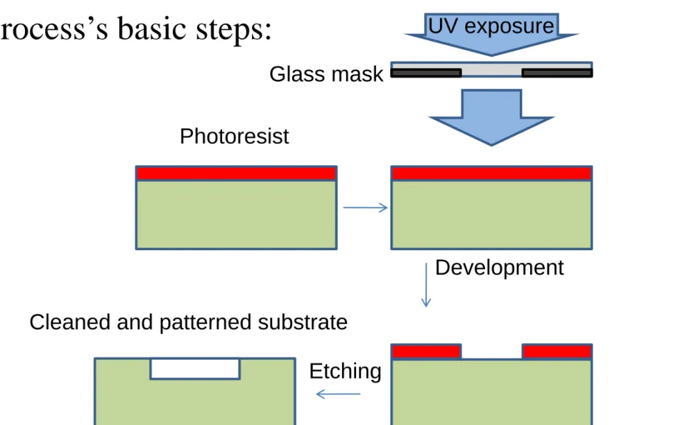
Illustration of the additive process’s basic steps:
Silicon wafer
Masking film (SiO2, Si3N4) Photoresist
Glass mask
UV exposure
Spin coat softbake
Development
Etching Cleaned and patterned film
Illustration of the subtractive process’s basic steps:
Photoresist
Glass mask
UV exposure
Development
Etching Cleaned and patterned substrate
Difficulties in lithography
• The features are smaller than the wavelength
• Diffraction limited resolution is the Rayleigh limit, as k1
*wavelength/NA, k1~0.61
• Solutions:
• Usage of local coherence (~0.5* wavelength / NA) for fine interference patterns – OPC
• Multiple exposure on the resists – double exposure and double patterning
• Phase shifting masks
• Solutions:
• Off-axis lighting (annular, dipole)
• Immersion lithography (larger NA)
• Multiple etching/lithography cycles
• Simply smaller wavelength light
• All of this solutions increase mask generation and processing, alignment, use extra steps and new
materials (like the photoresist).
• Immersion lithography (larger NA)
mask lithography
Without PSH With PSH
• Challenges
• Optical system is bulky, needs special optics, N2 atmosphere – optics of 0.10 nm rms
• Preprocessed or pre-distorted masks are needed, which requires large computational power
• Clean and low defect materials
• Above 45 nm node, the 248 nm wavelength must be used, powered by FrF lasers.
• The lithography below uses 193 nm wavelength, coming from ArF lasers. That is the practical limit (~22 nm) of this wavelength.
• State of the art of photolitography
• The next step is the extreme UV light. The next big step is to 13.5 nm.
• In EUV lithography the source (e.g. infrared laser bombarded tin droplets), the required power level is above 100W.
• High vacuum in the optical path.
• Mirrors instead of refractive optics. Polish surface precision:
100 pm across 300 mm, mirror positioning 1 um, even gravity a problem.
• Manufacturing and verification of masks (it needs the same EUV!)
Optical Proximity Correction (OPC)
• The Computational Lithography (CL) models the scanner, resist and etch process, and can correct for the deficiencies of the physical domain by correcting the shapes on the
mask.
• At 22 nm and below, the ability to draw circles and curvilinear shapes on a mask will become essential to enable OPC. That's very difficult because mask writing equipment draws rectangles and triangles.
Optical proximity correction
An illustration of optical proximity
correction. The blue shape is what is needed on the wafer, in green is the shape after applying optical
proximity correction, and the red contour is how the shape actually prints. The red shape is what would happened without predistorted mask.
Results of combining different techniques to form shapes under 65 nm
• OPC preprocessing, immersion optics
~60 nm
Alignment
• In order to make aligned patterns for different lithography steps that belong to a single structure must be correctly aligned to one another (nm precision over a 20-30 cm area!).
• The first pattern transferred to a wafer usually includes a set of alignment marks, which are high precision features that are used as the reference when positioning subsequent patterns. Often alignment marks are included in other
patterns,
Section III
Connection between manufacturing steps
and the design flow
Order of layer deposition:
1. Substrate doping during crystal growth
2. Well implants (single, dual, triple well structures) to form NMOST, PMOST, and floating noise free wells.
3. Highly doped metal to silicon contacts and active area.
4. Polysilicon gates.
5. Source/drain regions by polysilicon self-alignment.
6. Contacts on polysilicon and on substrate
7. Metal wires and contacts in between repetitively
Well implants
Polysilicon gates
Source/drain regions Highly doped active area.
Resulting in a very high density of wires. The SEM photo on the left shows a cross section of a 0.35 um technology with six metal layers.
Connection to drawing the desired layout in CAD tools.
• The low level design of devices and connections is equivalent to draw polygons of different materials.
• Several additional steps (masks) are generated automatically to help better alignment, easier drawing (e.g. where is no n-type doping is defined, automatically p-type will be applied).
Schematic of a circuit Layout of the circuit, as polygons
Connection to drawing the desired layout in CAD tools.
• There are tools that shows the 3D view of the drawn layout (all MEMS and 3D IC design tools)
Layout of the circuit, as polygons Cross-section of the wiring
3D IC process issues
• The true 3D integration is performed by through silicon vias (TSV), that connects thinned wafers.
• The difficulties arise from
• How to make thousands of deep holes and fill them with conductor?
• The solution is the Deep Reaction Ion Etching (DRIE), that capable of making 1:10…1:100 aspect ratio holes with 1-5 um aperture and 20- 100 um depth.
• 3D enabled CAD tools are limited in performance, and there is still no standardized handling of processes.
• Most successful solution is the predefined layer content, e.g.
Tezzaron Inc. offers such one.
Conclusions
• We went through the most important manufacturing steps of standard planar CMOS silicon technologies.
• Silicon wafer manufacturing
• Photolithography and its difficulties
• Visualization of the design flow at the bottom level
Recommended literature
IEEE Transactions on Semiconductor Manufacturing ISSN: 0894-6507
Published by: IEEE Solid-State Circuits Society
Semiconductor-Manufacturing.net
Your Guide to Semiconductor Manufacturing on the Web http://www.semiconductor-manufacturing.net/