Contents lists available atScienceDirect
Surface & Coatings Technology
journal homepage:www.elsevier.com/locate/surfcoat
Processing and characterization of a multibeam sputtered nanocrystalline CoCrFeNi high-entropy alloy film
P. Nagy
a,b,⁎, N. Rohbeck
a, G. Roussely
c, P. Sortais
c, J.L. Lábár
b,d, J. Gubicza
b, J. Michler
a, L. Pethö
aaEMPA Swiss Federal Laboratories for Materials Science and Technology, Laboratory for Mechanics of Materials and Nanostructures, Feuerwerkerstrasse 39, Thun CH- 3602, Switzerland
bDepartment of Materials Physics, Eötvös Loránd University, Budapest, Hungary
cPolygon Physics, 53 Rue des Martyrs, 38000 Grenoble, France
dInstitute for Technical Physics and Materials Science, Centre for Energy Research, Budapest, Hungary
A R T I C L E I N F O Keywords:
Physical vapor deposition High-entropy alloy Sputtering Microstructure Hardness
A B S T R A C T
Physical vapor deposition (PVD) is a well-known route for manufacturing hard coatings. In recent years, PVD has also been applied to create high-entropy alloy (HEA) thin films. HEAs are multicomponent alloys with nearly equal atomic fractions. To achieve the desired composition, typically alloy targets are used in the deposition process. The present work demonstrates that HEA thin films can also be processed using a multiple beam sputtering system in PVD, which does not require preliminary manufacturing of HEA targets, but rather uses commercially pure metal targets. The effectivity of this technique was demonstrated on a nanocrystalline CoCrNiFe HEA film with a thickness of about 1 μm. A part of the compositional gradient sample exhibited equal elemental fractions. The microstructure and the hardness of this part of the PVD film were studied in detail, and the results were compared with those obtained on a bulk nanocrystalline sample having the same chemical composition, but was prepared by the high pressure torsion (HPT) technique. The crystallite size and the texture were characterized by X-ray diffraction, while the hardness was measured by nanoindentation. The PVD film exhibited an exceptionally high hardness of 9.8 ± 0.3 GPa, a value that was notably higher than that de- termined for the HPT sample (7.3 ± 0.3 GPa). This study also demonstrated the capability of this new multiple beam sputtering technique for the production of compositional gradient samples with a wide range of elemental concentrations, enabling combinatorial analysis of multiple elements high-entropy alloy.
1. Introduction
High Entropy Alloys (HEAs) exemplify a recent development in materials science [1,2]. HEAs are intensively studied materials due to their impressive mechanical properties, such as very high strength even at high temperatures [3]. The synthesis of HEA materials exploits many different methods such as melt spinning [2], electromagnetic stirring [4], vacuum arc melting [5], or mechanical alloying [6]. In addition, severe plastic deformation (SPD) through high pressure torsion (HPT) technique was also applied on different HEA materials in order to ob- tain nanocrystalline microstructures [7–10].
In the last few years, some works reported successful synthesis of HEA thin films by physical vapor deposition (PVD) [11–13]. PVD is a well-known method to produce thin films and coatings. During this
process, atoms or molecules are deposited onto a surface from a solid or liquid source in a vacuum. Usually, the thickness of PVD thin films is between a few nanometers and a few micrometers. The main categories of PVD are ion plating, vapor deposition, arc deposition, vacuum de- position, and sputtering deposition. In the latter method, the deposited particles are vaporized from a surface (“target”) by a physical sput- tering process. Physical sputtering is a non-thermal vaporization pro- cess where the surface atoms are physically ejected from a solid surface by momentum transfer from atomic-sized energetic bombarding parti- cles, which are usually gaseous ions accelerated from a plasma [14].
Many industrial sectors and research fields apply versatile PVD tech- niques. Numerous PVD methods have been developed, such as in- ductively coupled plasma magnetron sputtering (ICP-MS), high power impulse magnetron sputtering (HIPIMS), self-sustained sputtering
https://doi.org/10.1016/j.surfcoat.2020.125465
Received 16 July 2019; Received in revised form 31 January 2020; Accepted 11 February 2020
⁎Corresponding author at: EMPA Swiss Federal Laboratories for Materials Science and Technology, Laboratory for Mechanics of Materials and Nanostructures, Feuerwerkerstrasse 39, Thun CH-3602, Switzerland.
E-mail address:nagyp@caesar.elte.hu(P. Nagy).
Available online 11 February 2020
0257-8972/ © 2020 The Author(s). Published by Elsevier B.V. This is an open access article under the CC BY license (http://creativecommons.org/licenses/BY/4.0/).
T
(SSS), and the hollow cathode magnetron (HCM) sputtering discharges.
For a detailed review, see [15] and the references therein.
Deposition of HEA thin films have already been demonstrated by different PVD methods in the literature. For instance, Gao et al. man- ufactured a CoCrNiAl HEA film via radio frequency (RF) magnetron sputtering PVD [11]. In another case, Nadutov et al. used cathodic arc evaporation (CEA) PVD to deposit AlFeCoNiCuCr HEA [12]. Tsau et al.
investigated the electrical resistance of HEA oxide thin films which were produced by oxidation of PVD HEA films [13]. The compositions of these HEA deposits were TiFeCoNiCu, TiFeCoNi and AlCrFeCoNiCu, where all targets were prepared by arc melting, and then vaporized by direct current (DC) PVD. In the work of Gao et al., the authors showed that HEA thin film samples had outstanding mechanical properties such as the high Young's modulus, and the hardness of the film was larger than the value measured on its bulk counterpart [11]. Moreover, the corrosion resistance of this PVD-processed HEA film was better than that for 304 stainless steel in a 3.5 wt% NaCl solution at room tem- perature [11]. Due to these impressive properties, HEA thin films pro- cessed by PVD are promising materials in many applications.
The effect of the chemical composition on the structure and prop- erties of HEA films can be studied on combinatorial samples. Recently, Marshal et al. reported the synthesis of a combinatorial HEA thin film by sputtering [16]. Formerly, PVD techniques developed for producing HEA layers used alloy targets in the deposition process. In this work, we aim to introduce a novel PVD method, which is suitable to create combinatorial HEA samples. Namely, a HEA thin film with the com- position of CoCrFeNi is produced using a multiple beam sputtering (MBS) system in PVD, which does not require preliminary manu- facturing of HEA targets, but rather uses commercially pure metal targets. The spatial distribution of the thickness and the chemical composition of the nanocrystalline CoCrFeNi thin film processed by MBS were also investigated. The grain and crystallite sizes as well as the texture for the equimolar CoCrFeNi composition were studied in detail.
The results were compared with those obtained on a bulk nanocrys- talline sample with the same chemical composition but processed by HPT.
2. Material and methods 2.1. The sputtering system
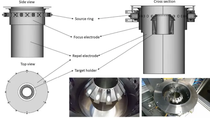
CoCrFeNi HEA thin film was processed by PVD using a Combimat Ion beam sputtering vacuum chamber manufactured by Polygon Physics. The experimental set up is exceptional among other PVD methods, because it can sputter twelve targets simultaneously (the number of targets can be increased up to twenty four). The vacuum chamber is a steel cube with the dimensions of 50 × 50 × 50 cm3, containing the sputtering system and the target holder. The diameter of the sputtering ring between the innermost electrodes is 32 cm. The
roots pump is capable of 15 m3/h pumping, and the turbomolecular pump capacity is 0.7 m3/s. The base vacuum in the chamber was 2 × 10⁻⁷ mbar. A schematic of the sputtering process is shown in Fig. 1.
The arrangement of the sputtering system is novel due to the compactness of the ion sources. The twelve ion sources form a ring, each one facing its own target, as shown inFig. 1. The ion energy is set by polarizing the source ring, and the ion beam shape can be controlled by polarizing the focus electrode. By controlling the ion beam shape, one can adapt the sputter spot size to the target size. These two po- larizations are obtained by using two independent high voltage supplies adjustable between 0 and 15 kV. In practice, the energy of the mono- charged ions produced by the sources can be tuned from 7 to 15 keV. At lower energy, the ion beams diverge and become wider than the targets used in the present experiment (it is possible to install larger targets).
The repel electrode is polarized to −400 V in order to deflect secondary electrons produced by the ions hitting the target (seeFig. 2). Without this repel electrode, the secondary electrons are accelerated backwards to the ion sources and could damage them. The targets are fixed on the target holder, which is a massive cooled aluminum block. The sample to be coated was placed 15 cm above the target holder.
In the present study, thin CoCrFeNi HEA layer was sputtered on a Si single crystal substrate with the diameter of 10 cm. The substrate was on ground potential during deposition to avoid charge accumulation.
The silicon wafer substrate exhibited good flatness and surface purity.
The deposition lasted 21 h. The present investigation focuses primarily on multiple beam sputtering as a candidate technology for combina- torial deposition of multicomponent thin films. Therefore, we did not investigate the adhesion between the substrate and the layer nor the effect of the substrate material on the layer microstructure in this study.
2.2. The ion source
The schematic of the ion source is shown inFig. 3. Each source is connected to an individual solid state high frequency generator sup- plying the power necessary to form the plasma. The typical power feeding of each source is in the order of 3 W. By tuning this power, the extracted ion current can be set within the range of 100–500 μA. The plasma sources utilize the phenomenon of electron cyclotron resonance (ECR) [17]. Three targets from each metal were placed nearby each other to create well-defined gradients in the sample.
The microstructure and mechanical characterization of the sput- tered film were carried out only on the part of the sample that has an equimolar CoCrFeNi composition. The results were compared with the properties of a bulk nanocrystalline CoCrFeNi HEA sample processed by HPT. The latter sample was prepared by vacuum induction melting and drop casting of a mixture of pure metals (purity > 99.9 wt%). A disk with a diameter of 10 mm and a thickness of ~0.85 mm was processed by HPT using a conventional facility with quasi-constrained set-up. The Fig. 1.Schematic showing the sputtering process. Only one source and one target are shown for the simplicity.
P. Nagy, et al. Surface & Coatings Technology 386 (2020) 125465
processing was performed at room temperature under the pressure of 6.0 GPa and at a rotation speed of 1 rpm for 20 turns [18].
2.3. Analysis of the chemical composition and the film thickness
The thickness and the chemical composition of the thin film sample were measured by an X-ray fluorescence (XRF) spectrometer (type: X- ray xdv-sdd, manufacturer: Fischerscope). The studied elements ranged from aluminum to uranium. The X-ray source was a microfocus tube with a tungsten anode. The detector was a Peltier-cooled Silicon Drift Detector (SDD). The thickness and the material composition were
investigated in 225 spots. Measurements were taken in a pattern con- sisting of 15 concentric circles with different radii. Each circle con- tained 15 measuring points. The diameter of each examined point was 1 mm.
2.4. Investigation of the microstructure
In the region of the PVD sample with equimolar composition, the microstructure was investigated by X-ray line profile analysis (XLPA) using an X-ray diffractometer operating at 30 kV and 25 mA with CoKα1 radiation (wavelength: 0.1789 nm) and a single crystal Ge Fig. 2.Schematic picture of the sputtering system.
Fig. 3.Schematic picture of the ion sources.
monochromator. The X-ray beam size was only 0.2 × 1 mm2. The microstructure was also studied by transmission electron mi- croscopy (TEM). A TEM-lamella was cut from the sample by focused ion beam (FIB) technique using Ga ions. First, a trench around the lamella was dug using 30 keV and 30 nA until a lamella thickness of about 4 μm was obtained. Then, a thinning process was performed at a voltage of 30 keV and a current of 7 nA until a lamella thickness of 1.5 μm was achieved. Finally, the lamella was cut and transferred to a grid, where it was further thinned at 16 keV and 50 pA, followed by polishing at 5 keV and 48 pA, and finished at 2 keV and 27 pA. TEM bright-field (BF) and dark-field (DF) images were taken by a Titan Themis G2 200 trans- mission electron microscope. The TEM images were recorded at 200 keV with a 4k*4k CETA 16 CMOS camera controlled by VELOX software.
The crystallographic texture of the sample was characterized by pole figure measurements using a Smartlab X-ray diffractometer (manufacturer: Rigaku, Japan) with CuKα radiation (wavelength:
0.15418 nm) and parallel-beam optics.
2.5. Nanoindentation
Nanoindentation measurements were performed using a Hysitron Ubi nanoindenter equipped with a diamond Berkovich tip. The max- imum load applied in these experiments was 3 mN in order to avoid exceeding a maximum penetration depth of 100 nm. The loading and unloading parts of indentation took 5–5 s and the holding time at the maximum load was 2 s. The hardness and the elastic modulus were determined by applying the Oliver-Pharr method [19]. The area func- tion for the tip had been calibrated carefully before the start of the measurements for the relevant measurement range. 25 indents were made on both the PVD film and the bulk sample to obtain a conclusive average.
3. Results and discussion
3.1. The spatial distribution of the film thickness and the chemical composition
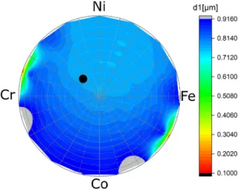
Fig. 4shows the thickness map of the thin film obtained by XRF. The average thickness of the sample was 0.799 μm with a standard devia- tion of 0.086 μm. The maximum thickness was measured as 0.916 μm close to the edge of the sample near the Co source. The variation of the thickness of the PVD film results from the different sputtering rates of the various targets.
The distribution of the concentrations of the constituents on the
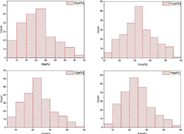
surface of the sample obtained by XRF is shown inFig. 5. Owing to the circular arrangement of the targets around the substrate and the plume shape sputtering, the elements show a gradient distribution. It is im- portant to note that due to the different sputtering rates, the place having equimolar composition slightly moved from the center towards the Co source as indicated by the black spot inFig. 5. The concentration distributions of the different elements are shown inFig. 6. The con- centration of each element varies in a range between ~5 and ~50 at.%.
The peaks of the concentration distributions can be found at ~25 at.%
for Cr and Fe while these peaks are at about 30 and 20 at.% for Co and Ni, respectively. The higher peak concentration for Co can be explained by its higher sputtering rate. The Ni source was located on the opposite side of the PVD chamber, which can explain its lower peak con- centration.
The equimolar concentration point can be found between the center of the wafer and the Co source. In this work, we investigate the mi- crostructure only in the spot corresponding to the equimolar CoCrFeNi because the results are intended to compare with the data available in the literature for the same HEA composition but processed by a dif- ferent technique. The width of this “equimolar concentration” spot was 1 mm, with the condition that the concentration of each element must be within the range of 24–26 at.%.
3.2. Crystallite size and texture of the equimolar CoCrFeNi film
The X-ray diffraction pattern taken in the part of the sample with equimolar composition indicated that the material is a single phase face centered cubic (fcc) structure. The full width at half maximum (FWHM = cosθ∗Δ2θ/λ, where θ is the Bragg angle of the reflection, Δ2θ is the breadth of the peak in radians and λ is the wavelength of X- rays) was determined for each peak and plotted as a function of the magnitude of the diffraction vector (g = 2∗sinθ/λ). These Williamson- Hall plots for the samples processed by PVD and HPT are shown in Fig. 7. Only slight differences were observed between the Williamson- Hall plots of the two samples. X-ray diffraction peaks can broaden due to the small crystallite size, the lattice defects such as dislocations and stacking/twin faults, as well as chemical heterogeneities [19]. A small spot size of the X-ray beam was selected (seeSection 2.4), and hence, the influence of chemical heterogeneities can be assumed to be mar- ginal. The contribution of lattice defects to peak broadening increases with increasing the magnitude of the diffraction vector. Thus, the ap- parent crystallite size (d) was determined as the reciprocal of the breadth of the first diffraction peak with the indices111(FWHM111) in accordance with the Scherrer formula [20]:
= d FWHM
1 .
111 (1)
The crystallite size for both, the PVD- and HPT-processed samples was determined to be around 20 nm, i.e., the two essentially different top-down and bottom-up methods gave similar microstructures.
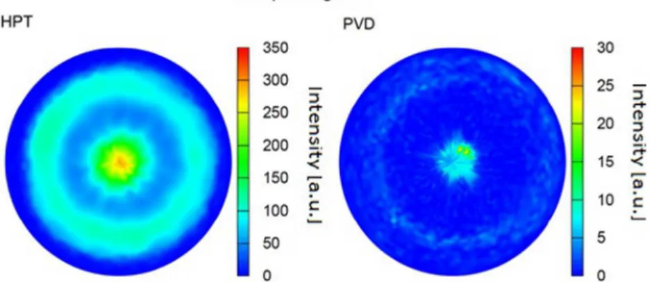
The 111 pole figures inFig. 8reveal that both PVD- and HPT-pro- cessed specimens exhibit similar textures where planes {111} are lying parallel to the sample surface. In the case of the HPT specimen, this texture was formed due to severe plastic deformation occurring during the 20 turns. For the PVD film, the 111 texture can be explained by the lowest surface energy if planes 111 are oriented parallel to the layer surface. The lower overall intensity in the pole figure of the PVD sample was caused by the smaller studied volume since the film thickness (~1 μm) was lower than the penetration depth of X-rays. Nevertheless, it is evident fromFig. 8that the texture is sharper for the PVD film than in the case of the HPT-processed CoCrFeNi HEA.
3.3. Study of the microstructure by TEM
Fig. 9a shows a BF image for the cross section of the PVD-processed HEA film at the equimolar concentration spot. The average thickness of Fig. 4.The thickness map of the thin film. The equimolar space is indicated by
a black spot.
P. Nagy, et al. Surface & Coatings Technology 386 (2020) 125465
the layer as determined from the TEM images was 720 nm, which is in good agreement with the value obtained by XRF technique (seeFig. 4).
The surface of the film was relatively smooth as revealed by the TEM image in Fig. 9a. The uncertainty of the layer thickness was about 10 nm which reflects the roughness of the film surface. The DF mi- crograph inFig. 9b reveals that the layer consists of columns perpen- dicular to the film surface with the thickness varying between 20 and 100 nm. The inset in Fig. 9b shows the corresponding selected area diffraction pattern. The development of the columnar grain structure can be explained by the oriented film growth perpendicular to the substrate surface during PVD. Fig. 9c and d show BF and DF TEM images, respectively, with higher magnification. The bright and dark spots inFig. 9d suggest that the columns are fragmented into grains/
subgrains. Their average size was found to be ~17 nm after studying about one hundred grains/subgrains. This value is in reasonable agreement with the crystallite size determined from the X-ray diffrac- tion peak breadth (~20 nm, seeSection 3.2).
Figs. 10a and b show BF and DF micrographs obtained for the bulk CoCrFeNi HEA sample processed by HPT. The average grain size was about 80 nm as determined from the TEM images. The inset inFig. 10b shows the corresponding selected area diffraction pattern. A part in Fig. 10b was magnified inFig. 10c, revealing that the grains consist of subgrains with a similar size as the crystallite size obtained by the analysis of the X-ray diffraction peak breadth (~20 nm). Thus, it seems that for both PVD- and HPT-processed samples the microstructure is fragmented into crystallites and the sizes of these crystallites are very similar for the two materials.
3.4. Comparison of the nanohardness obtained for PVD- and HPT- processed CoCrFeNi HEAs
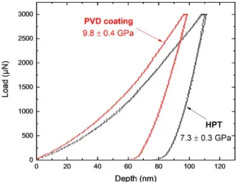
Fig. 11shows the load – penetration depth curves from the na- noindentation measurements. The Hysitron nanoindenter operates in load control mode and before starting the hardness tests, measurements with different loads have been performed in order to establish the load related to a maximum penetration depth of 100 nm. This depth value is about one order of magnitude smaller than the film thickness which guarantees to avoid any substrate effect on the measured hardness and elastic modulus.
The average hardness of the PVD film was 9.8 ± 0.4 GPa which is notably higher than that obtained for the bulk counterpart processed by HPT (7.3 ± 0.3 GPa). The higher hardness of the PVD sample cannot be attributed to any difference in the crystallite size or the defect densities (e.g., dislocation density or stacking fault and twin fault probabilities) since the PVD and HPT samples have very similar Williamson-Hall plots. TEM also revealed that the average size of the smallest microstructural units, i.e., the subgrains, is very similar for the two materials. At the same time, the pole figures inFig. 8indicate a significant difference between the textures of the two samples. Al- though, both samples have a 111 texture, the PVD film shows a sharper texture compared to the sample processed by HPT. This difference may cause the higher hardness of the PVD sample as 111 texture yields the highest hardening effect among all of the possible crystallographic di- rections if the material is loaded perpendicular to the investigated surface [21]. Indeed, former studies (e.g., [22]) showed that 111 Fig. 5.Color maps of the distribution of the concentrations of the constituents in the sample. The equimolar space is indicated by a black spot.
texture in fcc films yields a higher hardness compared to other pre- ferred crystallographic orientations. The Young's moduli determined from the present nanoindentation were 233 GPa and 276 GPa for the PVD film and the bulk HEA sample. Considering the error of these values (~10%), significant difference was not found between the moduli of the two samples. Moreover, these Young's moduli are close to the values calculated and measured for bulk CoCrFeNi HEA (250 ± 30 GPa) in the literature [23]. It seems that the elastic modulus is less sensitive to the 111 texture than the hardness for the present HEA which is in line with former studies. Indeed, it has been revealed that the weakening of 111 texture has a more pronounced effect on the flow stress through the variation of the Taylor factor than on the Young's modulus (compareFigs. 4 and 6in Ref. [21]). In addition, indentation
testing is a multiaxial deformation which also moderates the influence of texture on the measured modulus.
It should be emphasized that the present PVD sample exhibited a higher hardness than the values reported for CoCrFeNi HEA in previous studies. InTable 1, a direct comparison between the results obtained here and the literature data is given. Huo et al. [24] measured the hardness of equimolar CoCrFeNi samples processed by arc melting and subjected to tensile deformation. The obtained values were between 3.4 and 3.8 GPa, which are much lower than the hardness determined for the present PVD film. This difference can be explained by the much larger grain size (200–300 μm) of the arc melted samples compared to that of the films studied here (about 20 nm). In another study, Sa- thiyamoorthi et al. [25] fabricated CoCrFeNi composite samples with chromium-oxide and carbide particles using a combined approach of mechanical alloying (MA) of powders and subsequent spark plasma sintering (SPS). The grain size of the as-consolidated composite was
~120 nm and the hardness was measured to be about 5.7 GPa. In the present study, the much higher hardness can be attributed to the smaller grain size of ~20 nm and the 111 texture (see the previous paragraph). It should be noted, however, that the load applied during the hardness test also influences the measured hardness value. Due to the small thickness of the PVD film, only a low load (3 mN) could be applied during the hardness test. This force is orders of magnitude smaller than the loads used for bulk samples in the literature (see Table 1). Therefore, the so-called indentation size effect (ISE) might also contribute to the higher hardness measured in the present study.
The essence of this phenomenon is that the lower the load (and therefore the indentation size), the higher the hardness measured for the same material [26]. Nevertheless, the present study demonstrated the possibility of processing hard CoCrFeNi HEA film by multiple beam Fig. 6.The distribution of the concentrations of the four constituents in the PVD sample. These distributions were constructed from the color maps inFig. 5.
Fig. 7.The Williamson-Hall plot of the two CoCrFeNi HEA samples processed by PVD and HPT.
P. Nagy, et al. Surface & Coatings Technology 386 (2020) 125465
sputtering in PVD using commercially pure metal targets. As this novel technique produces combinatorial samples with a significant spatial distribution of constituents, the as-processed film allows to study the influence of chemical composition on the structure and properties of HEAs. Since the composition varies continuously in the as-processed samples, this method facilitates the effort towards finding the optimum composition with the required properties. This optimization process is easier and faster compared to other methods where for each composi- tion an individual sample must be prepared. It is also noted that the number of components can be scaled up to twelve as this PVD system can sputter twelve targets simultaneously. However, the main objective of this work was to demonstrate the ability of the present multi-beam sputtering technique to deposit HEA thin film systems. Therefore, only the spot with an equimolar composition was studied and compared
with a bulk counterpart processed by SPD. In our next study, the effect of the chemical composition on the structure and the hardness in the Co-Cr-Fe-Ni HEA system will be studied on a combinatorial sample processed with this new PVD technique.
4. Conclusions
The microstructure, the texture and the hardness of a CoCrFeNi HEA thin film processed by a novel multibeam sputtering PVD technique were investigated. This method does not require preliminary manu- facturing of HEA targets as it can sputter commercially pure metal targets. The following results were obtained:
1. The elements in the alloy have a well-defined gradient, which is the Fig. 8.111 pole figures for the two CoCrFeNi HEA samples processed by PVD and HPT.
Fig. 9.BF (a, c) and DF (b, d) TEM images taken on the cross section of the PVD-processed CoCrFeNi HEA film. The Si substrate is at the left side of the images in (a) and (b). The micrographs in (a) and (b) show the columnar microstructure while the images in (c) and (d) reveal the fragmentation of the col- umns into smaller grains/subgrains. The inset in (b) shows the corresponding selected area diffraction pattern. The arrow in the inset indicates the dif- fraction spot used for taking the DF images.
consequence of the specific geometry of the multiple beam sput- tering system. With the application of this PVD method, we created a CoCrFeNi HEA thin film with the thickness of about 1 μm. A spatial distribution of the elemental concentrations within the range of 5–50 at.% was observed. This new processing technique is cap- able of producing combinatorial samples that allows studying the effect of chemical composition on the structure and properties of multicomponent alloys (HEAs).
2. The hardness of the equimolar CoCrFeNi HEA thin film sputtered by this PVD method was 9.8 ± 0.4 GPa which is outstanding among the values obtained for similar CoCrFeNi HEAs processed by other
techniques in the literature. This exceptionally high hardness is likely due to the small grain size of ~20 nm. The reference sample was a HPT-processed bulk nanocrystalline CoCrFeNi HEA, which exhibited a lower hardness (7.3 ± 0.3 GPa) even though it had the same crystallite size. The significantly larger hardness of the PVD film was attributed to the sharper 111 texture developed due to the columnar growth of the layer.
Author contribution
P. Nagy: PVD, writing-original draft preparation N. Rohbeck: Nanoindentation
G. Roussely: Production of PVD equipment, Software for the PVD P. Sortais: Production of the PVD equipment
J.L. Lábár: TEM
J. Gubicza: XLPA, Pole figure, writing J. Michler: supervision
L. Pethö: PVD, writing
Data availability
The raw/processed data required to reproduce these findings cannot be shared at this time due to technical or time limitations.
Declaration of competing interest
The authors declare that they have no known competing financial interests or personal relationships that could have appeared to influ- ence the work reported in this paper.
Fig. 10.BF (a) and DF (b) TEM images taken on the bulk CoCrFeNi HEA sample processed by 20 turns of HPT. A magnified part of (b) is shown in (c) which suggests that the grains are fragmented into smaller subgrains. The inset in (b) shows the corresponding selected area diffraction pattern. The arrow in the inset indicates the diffraction spot used for taking the DF image.
Fig. 11.Load-penetration depth curves obtained by nanoindentation for the samples processed by PVD and HPT.
Table 1
Comparison between the grain sizes and the hardness values obtained in this study and the literature data for CoCrFeNi HEA. It is noted that the material listed in the second row of the table was a composite with HEA matrix and chromium-oxide and carbide particles which were formed during SPS sintering.
Reference Starting material Processing Grain size Hardness (load)
Huo et al. [22] Co-Cr-Fe-Ni high-purity metal Arc melting ~200–300 μm 3.4–3.8 GPa
(100 mN)
Sathiyamoorthi et al. [24] Co-Cr-Fe-Ni high-purity powder MA and SPS ~120 nm 5.7 GPa
(9.8 N)
Present work Co-Cr-Fe-Ni high-purity metal Multi ion beam sputtering ~20 nm 9.8 ± 0.4 GPa
(3 mN)
HPT ~20 nm (subgrain) 7.3 ± 0.3 GPa
(3 mN)
P. Nagy, et al. Surface & Coatings Technology 386 (2020) 125465
Acknowledgment
The authors are grateful to M. Kawasaki, J.-K. Han, Y. Zhao and Y.
Xue for the processing of the bulk sample by HPT, L. Illés for the pre- paration of the TEM lamella and to P.T. Hung for the X-ray diffraction measurement on the bulk sample. This work was carried out in the frame of the EUROSTARS programme through grant 10538 (COMBIMAT). This work was supported in part by the Ministry of Human Capacities of Hungary within the ELTE University Excellence program (1783-3/2018/FEKUTSRAT) and in part by the grant no.
VEKOP-2.3.3-15-2016-00002 of the European Structural and Investment Funds.
References
[1] J.-W. Yeh, S.-K. Chen, S.-J. Lin, J.-Y. Gan, T.-S. Chin, T.-T. Shun, C.-H. Tsau, S.- Y. Chang, Nanostructured high-entropy alloys with multiple principal elements:
novel alloy design concepts and outcomes, Adv. Eng. Mater. 6 (2004) 299–303, https://doi.org/10.1002/adem.200300567.
[2] B. Cantor, I.T.H. Chang, P. Knight, A.J.B. Vincent, Microstructural development in equiatomic multicomponent alloys, Mater. Sci. Eng. A 375–377 (2004) 213–218, https://doi.org/10.1016/j.msea.2003.10.257.
[3] Y. Zhang, T.T. Zuo, Z. Tang, M.C. Gao, K.A. Dahmen, P.K. Liaw, Z.P. Lu, Microstructures and properties of high-entropy alloys, Prog. Mater. Sci. 61 (2014) 1–93,https://doi.org/10.1016/j.pmatsci.2013.10.001.
[4] F. He, Z. Wang, S. Niu, Q. Wu, J. Li, J. Wang, C.T. Liu, Y. Dang, Strengthening the CoCrFeNiNb0.25 high entropy alloy by FCC precipitate, J. Alloys Compd. 667 (2016) 53–57,https://doi.org/10.1016/J.JALLCOM.2016.01.153.
[5] W.-R. Wang, W. Wang, S. Wang, Y. Tsai, C. Lai, J. Yeh, Effects of Al addition on the microstructure and mechanical property of AlxCoCrFeNi high-entropy alloys, Intermetallics 26 (2012) 44–51,https://doi.org/10.1016/J.INTERMET.2012.03.
[6] C. Wang, W. Ji, Z. Fu, Mechanical alloying and spark plasma sintering of005.
CoCrFeNiMnAl high-entropy alloy, Adv. Powder Technol. 25 (2014) 1334–1338, https://doi.org/10.1016/j.apt.2014.03.014.
[7] R. Valiev, Nanostructuring of metals by severe plastic deformation for advanced properties, Nat. Mater. 3 (2004) 511–516,https://doi.org/10.1038/nmat1180.
[8] A. Heczel, M. Kawasaki, J.L. Lábár, J. Jang, T.G. Langdon, J. Gubicza, Defect structure and hardness in nanocrystalline CoCrFeMnNi high-entropy alloy pro- cessed by high-pressure torsion, J. Alloys Compd. 711 (2017) 143–154,https://doi.
org/10.1016/j.jallcom.2017.03.352.
[9] D.H. Lee, M.Y. Seok, Y. Zhao, I.C. Choi, J. He, Z. Lu, J.Y. Suh, U. Ramamurty, M. Kawasaki, T.G. Langdon, J. Jang, Spherical nanoindentation creep behavior of nanocrystalline and coarse-grained CoCrFeMnNi high-entropy alloys, Acta Mater.
109 (2016) 314–322,https://doi.org/10.1016/j.actamat.2016.02.049.
[10] P.F. Yu, H. Cheng, L.J. Zhang, H. Zhang, Q. Jing, M.Z. Ma, P.K. Liaw, G. Liu, R.P. Liu, Effects of high pressure torsion on microstructures and properties of an Al0.1CoCrFeNi high-entropy alloy, Mater. Sci. Eng. A 655 (2016) 283–291,https://
doi.org/10.1016/j.msea.2015.12.085.
[11] L. Gao, W. Liao, H. Zhang, J. Surjadi, D. Sun, Y. Lu, Microstructure, mechanical and corrosion behaviors of CoCrFeNiAl0.3 high entropy alloy (HEA) films, Coatings 7 (2017) 156,https://doi.org/10.3390/coatings7100156.
[12] V.M. Nadutov, A.V. Proshak, S.Y. Makarenko, V.Y. Panarin, M.Y. Svavil’Nyj, Creation and Mössbauer studies of high-entropy physical vapor deposition by cathode arc evaporation (PVD CAE) coating AlFeCoNiCuCr, Mater. Werkst. 47 (2016) 272–277,https://doi.org/10.1002/mawe.201600489.
[13] C.H. Tsau, Y.C. Yang, C.C. Lee, L.Y. Wu, H.J. Huang, The low electrical resistivity of the high-entropy alloy oxide thin films, Procedia Engineering 36 (2012) 246–252, https://doi.org/10.1016/j.proeng.2012.03.037.
[14] D.M. Mattox, Handbook of Physical Vapor Deposition (PVD) Processing, William Andrew, New York, 1998,https://doi.org/10.1016/B978-081551422-0.50008-5.
[15] U. Helmersson, M. Lattemann, J. Bohlmark, A.P. Ehiasarian, J.T. Gudmundsson, Ionized physical vapor deposition (IPVD): a review of technology and applications, Thin Solid Films 513 (2006) 1–24,https://doi.org/10.1016/j.tsf.2006.03.033.
[16] A. Marshal, K.G. Pradeep, D. Music, L. Wang, O. Petracic, J.M. Schneider, Combinatorial evaluation of phase formation and magnetic properties of FeMnCoCrAl high entropy alloy thin film library, Sci. Rep. 9 (2019) 7864.
[17] T. Thuillier, L. Latrasse, J. Angot, J. Médard, T. Lamy, P. Sortais, Ultracompact/
ultralow power electron cyclotron resonance ion source for multipurpose applica- tions, Rev. Sci. Instrum. 81 (2010) 02B314, ,https://doi.org/10.1063/1.3272878.
[18] J. Gubicza, P.T. Hung, M. Kawasaki, J.-K. Han, Y. Zhao, Y. Xue, J.L. Lábár, Influence of severe plastic deformation on the microstructure and hardness of a CoCrFeNi high-entropy alloy: a comparison with CoCrFeNiMn, Mater. Charact. 154 (2019) 304–314,https://doi.org/10.1016/j.matchar.2019.06.015.
[19] G.M. Pharr, W.C. Oliver, An improved technique for determining hardness and elastic modulus using load and displacement sensing indentation experiments, J.
Mater. Res. 7 (1992) 1564–1583,https://doi.org/10.1557/JMR.1992.1564.
[20] J. Gubicza, X-ray Line Profile Analysis in Materials Science, IGI-Global, Hershey, 2014.
[21] B. Clausen, T. Lorentzen, T. Leffers, Self-consistent modelling of the plastic de- formation of F.C.C. polycrstals and its implications for diffraction measurements of internal stresses, Acta Mater. 46 (1998) 3087–3098,https://doi.org/10.1016/
S1359-6454(98)00014-7.
[22] L. Feng, Y.-Y. Ren, Y.-H. Zhang, S. Wang, L. Li, Direct correlations among the grain size, texture, and indentation behavior of nanocrystalline nickel coatings, Metals 9 (2019) 188.
[23] F. Tian, L.K. Varga, J. Shen, L. Vitos, Calculating elastic constants in high-entropy alloys using the coherent potential approximation: current issues and errors, Comput. Mater. Sci. 111 (2016) 350–358,https://doi.org/10.1016/j.commatsci.
2015.09.058.
[24] W. Huo, H. Zhou, F. Fang, X. Hu, Z. Xie, J. Jiang, Strain-rate effect upon the tensile behavior of CoCrFeNi high-entropy alloys, Mater. Sci. Eng. A 689 (2017) 366–369, https://doi.org/10.1016/j.msea.2017.02.077.
[25] P. Sathiyamoorthi, J. Basu, S. Kashyap, K.G. Pradeep, R.S. Kottada, Thermal sta- bility and grain boundary strengthening in ultrafine-grained CoCrFeNi high entropy alloy composite, Mater. Des. 134 (2017) 426–433,https://doi.org/10.1016/j.
matdes.2017.08.053.
[26] Y.V. Milman, A.A. Golubenko, S.N. Dub, Indentation size effect in nanohardness, Acta Mater. 59 (2011) 7480–7487,https://doi.org/10.1016/j.actamat.2011.08.
027.