hydrostatic pressure
Bálint Fülöp,1 Albin Márffy,1 Simon Zihlmann,2 Martin Gmitra,3 Endre Tóvári,1 Bálint Szentpéteri,1 Máté Kedves,1 Kenji Watanabe,4 Takashi Taniguchi,5 Jaroslav
Fabian,6 Christian Schönenberger,2 Péter Makk,1,∗ and Szabolcs Csonka1,†
1Department of Physics, Budapest University of Technology and Economics and Nanoelectronics “Momentum”
Research Group of the Hungarian Academy of Sciences, Budafoki út 8, 1111 Budapest, Hungary
2Department of Physics, University of Basel, Klingelbergstrasse 82, CH-4056 Basel, Switzerland
3Institute of Physics, Pavol Jozef Šafárik University in Košice, Park Angelinum 9, 040 01 Košice, Slovak Republic
4Research Center for Functional Materials, National Institute for Materials Science, 1-1 Namiki, Tsukuba 305-0044, Japan
5International Center for Materials Nanoarchitectonics,
National Institute for Materials Science, 1-1 Namiki, Tsukuba 305-0044, Japan
6Institute for Theoretical Physics, University of Regensburg, 93040 Regensburg, Germany (Dated: March 25, 2021)
Van der Waals heterostructures composed of multiple few layer crystals allow the engineering of novel materials with predefined properties. As an example, coupling graphene weakly to materials with large spin orbit coupling (SOC) allows to engineer a sizeable SOC in graphene via proxim- ity effects. The strength of the proximity effect depends on the overlap of the atomic orbitals, therefore, changing the interlayer distance via hydrostatic pressure can be utilized to enhance the interlayer coupling between the layers. In this work, we report measurements on a graphene/WSe2
heterostructure exposed to increasing hydrostatic pressure. A clear transition from weak localization to weak anti-localization is visible as the pressure increases, demonstrating the increase of induced SOC in graphene.
Keywords: hydrostatic pressure, spin orbit coupling, van der Waals heterostructure, graphene, WSe2
Graphene based van der Waals (vdW) heterostructures became one of the most studied physical systems in ma- terial science in recent years, which led to the emergence of designer electronics [1, 2]. Since the electrons are lo- calized at the surface for a single layer of graphene by definition, their properties can be easily modified by com- bining it with other few layer crystals leading to remark- able changes in its band structure. A prominent example is the moiré effect caused by the rotation (and possible small lattice mismatch) of the graphene and the underly- ing other lattice. This led to the Hofstadter physics and formation of secondary charge neutrality points (CNPs) when graphene is placed on hexagonal boron nitride (hBN) [3–10]; whereas correlated phases including su- perconductivity, correlated insulators or ferromagnetic states have been found if it is placed on another graphene sheet [11–14]. Graphene based heterostructures are also promising building blocks for spintronic devices [15–17].
Although graphene is known to provide very long spin lifetimes [18, 19], the absence of spin orbit coupling (SOC) also hinders electrical control and charge to spin conversion in it. However, a large SOC can be induced in graphene by proximity effect if placed on a transition metal dichalcogenide (TMDC) flake [20–22], which can lead to topologically nontrivial states and the quantum spin Hall effect [23]. Recently, a wide range of exper- iments demonstrated the presence of proximity-induced SOC in various heterostructures by weak-localization, ca- pacitance or spin transport measurements, and it has
d kerosene
hBN
WSe2 Cr/Au
SiO2 Si G
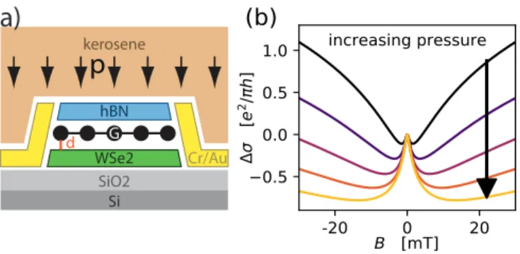
p a)
FIG. 1. (a) Schematic side view of a hBN/graphene/WSe2
heterostructure in kerosene pressure transfer medium. Hydro- static pressure reduces the distancedbetween the graphene and the WSe2 layers (among others), which leads to an en- hancement of the proximity-induced SOC in graphene. (b) Simulated weak anti-localization curves using realistic param- eters to demonstrate the potential effect of the application of ca. 2 GPa pressure on the heterostructure. The increased SOC leads to a more pronounced WAL peak in the magneto- conductivity curve. See the Supp. Mat. for the simulation details.
been found that Rashba and valley–Zemann-like SOC is induced in graphene leading to a large spin relaxation anisotropy [24–35]. Since this enhancement of SOC origi- nates from the hybridization of graphene’sπorbitals with the TMDC layer’s outer orbitals, the strength of the SOC depends strongly on the overlap of the orbital wavefunc- tions and, therefore, on the interlayer distance, which is
arXiv:2103.13325v1 [cond-mat.mes-hall] 24 Mar 2021
2
2.5 0.0 2.5 5.0 7.5 10.0 12.5 15.0
V
g[V]
2 4 6 8 10 12
G [e
2/h ]
no pr.
0.6 GPa 1.2 GPa 1.8 GPa
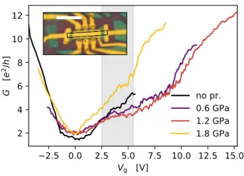
FIG. 2. Two-terminal conductance vs. back gate voltage measurements at different pressures. The curve minima, as- sumed to be the CNP, are shifted to Vg = 0 to maintain comparability of the curve shapes. The area considered for the comparison of the WAL signals, between 2.5 V and 5.5 V, is highlighted by the gray background. Inset: Optical micro- graph of the sample. Scale bar is 10 µm. The highlighted segment is measured in two-terminal measurements at 1.5 K for all pressures.
determined by the van der Waals force. Compressing such a heterostructure by applying an external pressure (see Figure 1a), is expected to increase the SOC, which can be captured by weak localization measurements, as shown by simulated magneto-conductivity curves in Fig- ure 1b [21, 36].
In this work we present experimental evidence of ma- nipulation of the interlayer coupling and the proximity SOC in a graphene/WSe2 heterostructure using hydro- static pressure. The pressure control adds another knob with which the electronic properties of 2D materials can be engineered, allowing to more robust proximity states or even engineer novel states of matter.
The illustration of the studied device is shown in Fig- ure 1a, whereas an optical image is given in the inset of Figure 2. The heterostructure is built on a Si/SiO2
substrate using the dry stacking assembly method [37], where the heavily-doped silicon layer was used as a global back gate. It consists of a monolayer graphene, which is on top of a very thin (3 nm) WSe2 flake providing the spin orbit coupling, and covered with a hexagonal boron nitride (hBN) flake to protect it from the kerosene pres- sure medium [38] (see Figure 1a). The heterostructure is shaped into a Hall bar and contacted using 1D Cr/Au electrodes [39] (see Figure 2 inset). The total length of the graphene segment was L = 8.3 µm, and the width was W = 1.1 µm. The device is also equipped with a top gate extending over the major part of the measured segment but it was grounded during the measurements.
Another sample, showing similar behaviour is shown in
the Supp. Mat.
The wafer carrying the device was cut tightly and bonded on a special high pressure sample holder, then placed in kerosene environment in a piston-cylinder hy- drostatic pressure cell. The setup is designed to overcome the technical difficulties of electronic measurements of nanocircuits in a hostile environment [38]. Low tempera- ture (1.5 K) measurements have been carried out at four different hydrostatic pressure settings in increasing order (no pressure, 0.6 GPa, 1.2 GPa, 1.8 GPa). Each pressure change involved warming up the sample to room tem- perature, applying the pressure using a hydraulic press, clamping the pressure cell, and cooling the sample down again. Measurements were carried out by standard lock- in technique at f = 177 Hz with an AC bias voltage VAC = 100 µV and an external low-noise current ampli- fier.
We characterized our devices by measuring the two- terminal conductance as a function of back gate voltage at each pressure, as shown in Figure 2. The measured segment is highlighted in the inset. The CNP position was found at slightly differentVg back gate voltages in each case but remained between -5.2 V and -0.6 V, which was corrected by shifting the curve minima to Vg = 0 for further use. The curves are quite similar in shape, with a minimum around the CNP. Using a simple paral- lel plate capacitor model for the estimation of the charge carrier densityn(Vg), field effect mobility was calculated based on a linear fit on the two-terminal conductance.
Electron mobility values were found between 11,000 and 24,000 cm2V−1s−1 without any systematic dependence on the applied pressure. A change in the scattering pro- cesses and the observed field effect mobility is not un- usual in case of vdW heterostructures during subsequent cooldowns even without applied pressure and can be at- tributed to the rearrangement of scattering centers. Thus we conclude that the sample conductance and quality is not significantly affected by the applied pressure.
Now we turn to low-field magneto-conductance mea- surements. Weak localization is a low temperature quantum correction to the magneto-conductance of dif- fusive samples and expected to show a conductance minimum (weak localization, WL) or maximum (weak anti-localization, WAL) at zero field depending on the strength of SOC[40].
We have recorded the two-terminal conductance curves as the B field was swept in a range of±30 mT for several gate voltages, both in the up and down magnet ramp- ing direction. At each gate voltage, we symmetrized the curves, then subtracted the zero-field conductance from the measured curve leading to 2D conductance maps
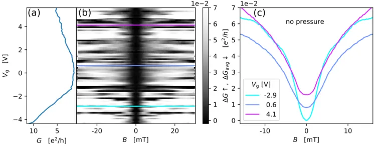
∆G(Vg, B). The zero-field conductance against the gate voltage for the no pressure case is plotted in Figure 3a.
The corresponding conductance map is shown in Figure 3b, where a vertical dark gray line alongB = 0 appears due to the correction method, and lighter gray tones on
5 10 G [e
2/h]
4 2 0 2 4
V
g[V ]
(a)
-20 0 20
B [mT]
(b)
-10 0 10
B [mT]
0 1 2 3 4 5 6 7
G , G
avg[e
2/h ]
1e 2
no pressure
(c)
V
g[V]
-2.9 0.6 0 4.1
1 2 3 4 5 6 1e 2 7
FIG. 3. Weak localization measurement at ambient pressure. (a) Zero-field conductance G(Vg, B = 0), used to extract D andτia, as detailed in the text. (b) 2D grayscale plot of the two-terminal conductance corrected by the zero-field conductance
∆G(Vg, B) =G(Vg, B)−G(Vg, B= 0). (c) Two-terminal magneto-conductance at fixed gate voltages marked in panel b with
±1.5 V averaging along the vertical axis to reduce the effect of UCF. The curves are shifted by 0.01e2/h for clarity. At small magnetic fields (B <5 mT) the well-formed conductance dip corresponds to weak localization (WL) effect that is present at all gate voltages, although the curve shape changes slightly. At higher fields (B >5 mT) the influence of UCF leads to irregular line shapes and were not analysed in the current work.
each side are a sign of positive magneto-conductance cor- responding to WL. At higher magnetic fields, universal conductance fluctuations [40] (UCF) of amplitude up to 0.4 e2/h across the gate voltage axis are also visible on the map as saturated horizontal lines. To increase visibility of WAL signal, an averaging on a gate range of ±1.5 V was applied on the conductance, noted as ∆Gavg(Vg, B).
Cuts of ∆Gavg at fixed Vg values are shown in fig 3c.
All these cuts show a WL dip with slight changes in the curve shape as a function of the gate voltage. Here, the absence of a WAL peak suggest a weak SOC, which will be discussed later. This is in agreement of previous mea- surements on this device in the Supp. Mat. of Ref. [31].
After having performed the above procedure for each pressure, we selected the curves at 4±1.5 V, i.e. aver- aging the ∆G(Vg, B) curves between 2.5 V and 5.5 V for all the pressures. We assume the characteristic times of the scattering processes do not change much across the gate range where the averaging is performed, while the contribution of UCF is reduced. The conductance was converted to conductivity for the extraction of scattering time scales by curve fitting. Background signal was also recorded simultaneously with the localization measure- ment and found to be constant, see the Supp. Mat. for details.
Our main findings are presented in Figure 4a, where the averaged magneto-conductivity ∆σavg(Vg = 4 V, B) for all four pressures is plotted for low magnetic fields.
The initial curve, at ambient pressure, shows a wide con- ductivity dip, which gets wider as the pressure increases
to 0.6 GPa, and a sharp central peak appears at higher pressures. This transition of WL to WAL is a clear sig- nature of the increasing proximity-induced SOC in the graphene layer. This tendency is robust for the entire gate voltage range as shown by the cuts at different gate voltages in Figure 4b. See the Supp. Mat. for the full comparison of all pressures at various gate voltages. To quantitatively demonstrate this transition, the data was fitted using the McCann-Falko weak anti-localization for- mula [41]:
∆σ(B) =−1 2
e2 πh
F
τB−1 τϕ−1
−F
τB−1 τϕ−1+ 2τasy−1
−2F τB−1 τϕ−1+τasy−1+τsym−1
,
(1)
where ∆σ(B) = σ(B)−σ(B = 0) is the correction to the magneto-conductivity. We introduced the function F(x) = ln(x) +ψ(0.5 +x−1) withψbeing the digamma function and h being the Planck’s constant. The rate τB−1 = 4eDB/~ is associated to the magnetic field with D, the diffusion constant. τϕis the phase-breaking time, τasy is the scattering time due to SOC terms that are asymmetric upon z/-z inversion, andτsym is the corre- sponding time due to terms invariant under z/-z inver- sion. Using the previously calculated charge carrier den- sityn(Vg), the Fermi velocity of graphene, and the Ein- stein relation, the diffusion constant and the momentum relaxation time can be extracted from the gate voltage
4
-2 0 2
B [mT]
1 0 1 2 3 4
avg
[e
2/h ]
1e 1 (a) no pr.
0.6 GPa 1.2 GPa 1.8 GPa Fit
-20 -10 0 10 20
B [mT]
1 0 1 2 3 4 5
G
avg[e
2/h ]
1e 2 (b) 1.8 GPa -2 V 1 V 4 V 7 V
no pr. 0.6 GPa 1.2 GPa 1.8 GPa 250
300 350 400 450 500
R
[ eV ]
(e)
3-parameter 5-parameter no pr. 0.6 GPa 1.2 GPa 1.8 GPa
10
1210
810
4sym
[s] (d)
0.2 0.4 0.6 0.8 1.0
[s]
1e 11
(c)
asy
FIG. 4. (a) Comparison of averaged ∆σavg(B) measurement curves for each pressure at 4 V. Clear signature of the WL→ WAL evolution is visible. Solid blue lines forB >0: fits using Equation 1. (b) Two-terminal magneto-conductance for 1.8 GPa pressure at fixed gate voltages with±1.5 V averaging to reduce the effect of UCF, similarly to 3c. The WAL peak observed in panel a is present at all gate values with changing amplitude but the width staying approximately the same. At higher fields (B > 5 mT) the influence of UCF is still dominant. (c) Summary plot of the fit values of τϕ, τasy. The errorbars represent uncertainty assessed by our method detailed in the Supp. Mat. Decreasingτasywith increasing pressure indicates the presence of an increasing Rashba SOC and interlayer coupling strength between graphene and WSe2. (d) Fit values ofτm. Due to the large uncertainty, the value of this parameter cannot be extracted. (e)λR parameter for each pressure, calculated using the previously extracted parameter values forτasy andτm. Calculated values based on the 3-parameter formula (Equation 1) are plotted with orange, and values based on the 5-parameter formula are plotted with green (see the Supp. Mat. for details). A clear growing tendency proves the enhancement of the proximity SOC induced by the WSe2 layer. The data points are slightly shifted horizontally to avoid overlapping errorbars.
curves and were found betweenD= 0.07–0.12 m2s−1and τm= 1.3–2.4·10−13s for all pressure measurements with- out any systematic pressure dependence, but in correla- tion with the field effect mobility. Since τm is expected to be the shortest amongst the time scales, we set it as the lower bound for all fitting time parameters. Equa- tion 1 is valid if the intervalley scattering timeτivis much shorter than the times corresponding to SOC, therefore the contribution of the effect of the charge carriers’ chi- ral nature can be neglected. We also performed fits with a more complex, 5-parameter fitting formula including theτiv intervalley andτia intravalley scattering times as fitting parameters, which suggest that τiv is indeed at least an order of magnitude smaller than the other fitted time scales, supporting the validity of Equation 1 (see the Supp. Mat.).
In Figure 4a, fit curves are plotted using solid blue lines. The extracted fit parameters are summarised in Figure 4c-d. A clear tendency of the reduction of τasy
can be observed as its value decreases from 7.4·10−12s to 2.7·10−12s as the pressure increases to 1.8 GPa. This is a reduction by a factor of 2.7 and corresponds to an increasing SOC. This is the main proof to our ini- tial expectation of increasing interlayer coupling. The phase-breaking time, τϕ, also shows a moderately de- creasing but fluctuating trend with pressure, obtaining values from 9.2·10−12s to 5.5·10−12s, staying well above
τasy at all pressures. The reason for this decreasing ten- dency is unclear at the moment. The third fit parameter, τsym, obtains fit values that are much longer thanτϕand the fit errors are more than an order of magnitude large (see Figure 4d), which means that it has negligible effect on the magneto-conductance curve. Therefore, although there seems to be a decreasing trend in the lifetime, we can not extract any reliable value for it at any pressure.
Discussion on this result will be given later.
The spin relaxation times can be connected to band structure parameters via spin relaxation mechanisms. It has been established that two relevant spin orbit terms are formed in graphene/TMDC heterostructures. One of them is the Rashba term, described by the Hamiltonian HR =λR(κσxsy−σysx) [42], which corresponds to the breaking of the lateral mirror symmetry due to the differ- ence of the hBN and TMDC neighbouring layers to the graphene sheet. Its strength is set by theλR parameter, κ= ±1 for the K and K’ valleys, the Pauli matrices σ are acting on the lattice pseudospin, andkx, ky are the electron wave vector components measured from the K (K’) points. This term leads to relaxation processes that are contained inτasyvia the Dyakonov–Perel mechanism, from which the Rashba parameter can be expressed as λR=~2q
τm−1τasy−1[43].
The increasing scattering rates lead to an increase in the Rashba parameter, which clearly demonstrates that
we were able to tune the strength of the induced SOC.
The values are summarised in Figure 4e, shown by the or- ange curve. We have also plotted the value of the Rashba parameter from the 5-parameter fitting formula in green (see Supp. Mat.), which is in agreement with the values from the simplified formula within the error limits.
The second dominant spin orbit term in these sys- tems is theHVZ=λVZκσ0szvalley–Zeeman term, where λVZ characterizes the coupling strengh. This term cor- responds to an effective Zeeman magnetic field which is opposite in the two valleys due to inversion symmetry breaking, but still preserving time reversal symmetry. It leads to relaxation contained in theτsym via a modified Dyakonov–Perel mechanism, where the intervalley scat- tering time,τiv, enters instead of the momentum scatter- ing time: λVZ= ~2q
τiv−1τsym−1.
The strength of the valley–Zeeman coupling cannot be extracted reliably in our experiments due to the uncer- tainty in τsym. The mean values from the fit show a slightly increasing trend and would give 4 µeV and 23 µeV for the lowest and highest pressure, respectively, but even taking the smallest obtained values fromτsym, we arrive at values between 140 and 440 µeV.
In order to quantify changes in the Rashba parameter and to compare it to expectations, we have performed ab initio calculations following our previous results in Ref. [20, 21]. Using a structural supercell model of 4×4 graphene and 3×3 WSe2 with relaxed lateral atomic positions, 5%/GPa compressibility for the layer distance between the graphene and WSe2 layers was found. The applied 1.8 GPa pressure induces 9% compression in the z direction that leads to an increment of the calculated Rashba energy from 600 µeV to 1.8 meV and of the cal- culated valley–Zeeman energy from 1.2 meV to 3.0 meV.
As plotted in Figure 4e, the value of the Rashba energy λRincreases from 0.3 meV to 0.5 meV, which is in the or- der of magnitude of the expected values, although slightly lower than them. The values of the valley–Zeeman en- ergy are much smaller than expected theoretically.
Several reasons might be behind these low SOC values relative to the theoretical expectations. One possibility is that the interfaces are not clean enough and some con- tamination is trapped in-between, which would lower the strength of the spin orbit coupling. Another difference from other samples [31] might come from the relative ori- entation of the graphene and the WSe2. It has been the- oretically found [44, 45] that the rotation angle strongly modulates the strength of the SOC and for certain angles the SOC almost disappears. Since we did not control the twist angles between the layers during fabrication, they may have aligned such a way that it would lead to re- duced SOC. The rotation angle affects the Rashba and the valley–Zeeman coupling in a different way, which can explain why we see stronger suppression for theλVZthan forλR, and why the former deviated between measured
and simulated values. Finally, we note that the strength of SOC obtained from these formulas might also depend on how well the UCF is removed during averaging. This can be seen in Figure 4b, where the different gate val- ues lead to slightly different magneto-conductance trend.
We stress here that although the absolute value of the extracted parameters have to be taken with care, the tendency visible in Figure 4a clearly shows that the pres- sure indeed leads to an increase of the SOC. We do not expect that the twist angle is modulated by the applied pressure [46]; nor the functional form of the angle depen- dence is modified by it, only the overall strength of the SOC is affected.
In conclusion, we studied for the first time the effect of hydrostatic pressure on WL signal in graphene/TMDC heterostructure. We demonstrated the enhancement of the proximity-induced SOC using hydrostatic pressure.
Our analysis of the measured signals supports an increas- ing SOC and is in qualitative agreement with theoreti- cal expectations. The strength of SOC is an important parameter in graphene spintronics, since it determines charge to spin conversion efficiencies and also plays a cen- tral role in graphene–TMDC optoelectronic devices [20].
Our work also points out that hydrostatic pressure can be generally used to change the interlayer distance up to a remarkable 10%, which provides a new way to boost proximity effects in van der Waals heterstructures, e.g.
exchange interaction induced into graphene [47–50], or into TDMCs [51, 52], furthermore, a strong proximity ef- fect on correlated magic angle twistronics devices [53, 54], or to stabilize fragile states like the topological insulator phase in graphene-TDMC heterostructures [33].
AUTHOR CONTRIBUTIONS
S.Z, M.K and P.M. fabricated the devices. Measure- ments were performed by B.F., A.M. with the help of E.T., B.Sz. B.F. did the data analysis. M.G. did the the- oretical calculation. B.F. and P.M. and Cs.Sz. wrote the paper and all authors discussed the results and worked on the manuscript. K.W. and T.T. grew the hBN crys- tals. The project was guided by Sz.Cs., P.M, C.S. and J.F.
ACKNOWLEDGMENTS
This work acknowledges support from the Topograph FlagERA network, the OTKA FK- 123894 grants, the Swiss Nanoscience Institute (SNI), the ERC project Top- Supra (787414), the Swiss National Science Foundation, the Swiss NCCR QSIT. This research was supported by the Ministry of Innovation and Technology and the National Research, Development and Innovation Office within the Quantum Information National Laboratory
6 of Hungary and by the Quantum Technology National
Excellence Program (Project Nr. 2017-1.2.1-NKP-2017- 00001), by SuperTop QuantERA network, by the FET Open AndQC netwrok and Nanocohybri COST network.
P.M. and E.T. received funding from Bolyai Fellowship.
M.G. acknowledges Scientific Grant Agency of the Min- istry of Education of the Slovak Republic under the contract No. VEGA 1/0105/20. K.W. and T.T. ac- knowledge support from the Elemental Strategy Initia- tive conducted by the MEXT, Japan, Grant Number JPMXP0112101001, JSPS KAKENHI Grant Numbers JP20H00354 and the CREST(JPMJCR15F3), JST.
The authors thank Andor Kormányos, András Pályi and Péter Boross for fruitful discussions, and Márton Ha- jdú, Ference Fülöp team for their technical support.
∗ peter.makk@mail.bme.hu
† csonka@mono.eik.bme.hu
[1] Geim, A. K.; Grigorieva, I. V. Van der Waals heterostruc- tures.Nature2013,499, 419–425.
[2] Giustino, F. et al. The 2021 quantum materials roadmap.
Journal of Physics: Materials 2021,3, 042006.
[3] Dean, C. R.; Wang, L.; Maher, P.; Forsythe, C.; Gha- hari, F.; Gao, Y.; Katoch, J.; Ishigami, M.; Moon, P.;
Koshino, M.; Taniguchi, T.; Watanabe, K.; Shep- ard, K. L.; Hone, J.; Kim, P. Hofstadter’s butterfly and the fractal quantum Hall effect in moiré superlattices.
Nature2013,497, 598.
[4] Ponomarenko, L. A. et al. Cloning of Dirac fermions in graphene superlattices.Nature2013,497, 594–597.
[5] Hunt, B.; Sanchez-Yamagishi, J. D.; Young, A. F.;
Yankowitz, M.; LeRoy, B. J.; Watanabe, K.;
Taniguchi, T.; Moon, P.; Koshino, M.; Jarillo-Herrero, P.;
Ashoori, R. C. Massive Dirac Fermions and Hofstadter Butterfly in a van der Waals Heterostructure. Science 2013,340, 1427.
[6] Krishna Kumar, R. et al. High-temperature quantum os- cillations caused by recurring Bloch states in graphene superlattices.Science2017,357, 181.
[7] Krishna Kumar, R.; Mishchenko, A.; Chen, X.;
Pezzini, S.; Auton, G. H.; Ponomarenko, L. A.;
Zeitler, U.; Eaves, L.; Fal’ko, V. I.; Geim, A. K. High- order fractal states in graphene superlattices.Proc Natl Acad Sci USA2018,115, 5135.
[8] Wang, L.; Zihlmann, S.; Liu, M.-H.; Makk, P.; Watan- abe, K.; Taniguchi, T.; Baumgartner, A.; Schönen- berger, C. New Generation of Moiré Superlattices in Doubly Aligned hBN/Graphene/hBN Heterostructures.
Nano Lett.2019,19, 2371–2376.
[9] Wang, Z. et al. Composite super-moiré lattices in double- aligned graphene heterostructures. Sci Adv 2019, 5, eaay8897.
[10] Yankowitz, M.; Ma, Q.; Jarillo-Herrero, P.; LeRoy, B. J.
van der Waals heterostructures combining graphene and hexagonal boron nitride.Nature Reviews Physics 2019, 1, 112–125.
[11] Cao, Y.; Fatemi, V.; Fang, S.; Watanabe, K.;
Taniguchi, T.; Kaxiras, E.; Jarillo-Herrero, P. Unconven-
tional superconductivity in magic-angle graphene super- lattices.Nature2018,556, 43.
[12] Cao, Y.; Fatemi, V.; Demir, A.; Fang, S.;
Tomarken, S. L.; Luo, J. Y.; Sanchez-Yamagishi, J. D.;
Watanabe, K.; Taniguchi, T.; Kaxiras, E.; Ashoori, R. C.;
Jarillo-Herrero, P. Correlated insulator behaviour at half-filling in magic-angle graphene superlattices.Nature 2018,556, 80.
[13] Sharpe, A. L.; Fox, E. J.; Barnard, A. W.; Finney, J.;
Watanabe, K.; Taniguchi, T.; Kastner, M. A.;
Goldhaber-Gordon, D. Emergent ferromagnetism near three-quarters filling in twisted bilayer graphene.Science 2019,365, 605.
[14] Lu, X.; Stepanov, P.; Yang, W.; Xie, M.; Aamir, M. A.;
Das, I.; Urgell, C.; Watanabe, K.; Taniguchi, T.;
Zhang, G.; Bachtold, A.; MacDonald, A. H.; Efe- tov, D. K. Superconductors, orbital magnets and cor- related states in magic-angle bilayer graphene. Nature 2019,574, 653–657.
[15] Han, W.; Kawakami, R. K.; Gmitra, M.; Fabian, J.
Graphene spintronics.Nat Nano2014,9, 794–807.
[16] Avsar, A.; Ochoa, H.; Guinea, F.; Özyilmaz, B.; van Wees, B. J.; Vera-Marun, I. J. Colloquium: Spintronics in graphene and other two-dimensional materials. Rev.
Mod. Phys.2020,92, 021003.
[17] Hu, G.; Xiang, B. Recent Advances in Two-Dimensional Spintronics.Nanoscale Research Letters2020,15, 226.
[18] Kamalakar, M. V.; Groenveld, C.; Dankert, A.;
Dash, S. P. Long distance spin communication in chemi- cal vapour deposited graphene.Nature Communications 2015,6, 6766.
[19] Drögeler, M.; Franzen, C.; Volmer, F.; Pohlmann, T.;
Banszerus, L.; Wolter, M.; Watanabe, K.; Taniguchi, T.;
Stampfer, C.; Beschoten, B. Spin Lifetimes Exceeding 12 ns in Graphene Nonlocal Spin Valve Devices.Nano Lett.
2016,16, 3533–3539.
[20] Gmitra, M.; Fabian, J. Graphene on transition-metal dichalcogenides: A platform for proximity spin-orbit physics and optospintronics. Phys. Rev. B 2015, 92, 155403.
[21] Gmitra, M.; Kochan, D.; Högl, P.; Fabian, J. Trivial and inverted Dirac bands and the emergence of quantum spin Hall states in graphene on transition-metal dichalco- genides.Phys. Rev. B 2016,93, 155104.
[22] Garcia, J. H.; Cummings, A. W.; Roche, S. Spin Hall Ef- fect and Weak Antilocalization in Graphene/Transition Metal Dichalcogenide Heterostructures. Nano Lett.
2017,17, 5078–5083.
[23] Kane, C. L.; Mele, E. J. Quantum Spin Hall Effect in Graphene.Phys. Rev. Lett.2005,95, 226801.
[24] Avsar, A.; Tan, J. Y.; Taychatanapat, T.; Balakrish- nan, J.; Koon, G. K. W.; Yeo, Y.; Lahiri, J.; Car- valho, A.; Rodin, A. S.; O’Farrell, E. C. T.; Eda, G.; Cas- tro Neto, A. H.; Özyilmaz, B. Spin-orbit proximity effect in graphene.Nature Communications2014,5, 4875.
[25] Wang, Z.; Ki, D.-K.; Chen, H.; Berger, H.; MacDon- ald, A. H.; Morpurgo, A. F. Strong interface-induced spin-orbit interaction in graphene on WS2.Nature Com- munications2015,6, 8339.
[26] Wang, Z.; Ki, D.-K.; Khoo, J. Y.; Mauro, D.; Berger, H.;
Levitov, L. S.; Morpurgo, A. F. Origin and Magnitude of
‘Designer’ Spin-Orbit Interaction in Graphene on Semi- conducting Transition Metal Dichalcogenides.Phys. Rev.
X 2016,6, 041020.
[27] Yang, B.; Tu, M.-F.; Kim, J.; Wu, Y.; Wang, H.; Al- icea, J.; Wu, R.; Bockrath, M.; Shi, J. Tunable spin- orbit coupling and symmetry-protected edge states in graphene/WS 2.2D Materials2016,3, 031012.
[28] Ghiasi, T. S.; Ingla-Aynés, J.; Kaverzin, A. A.;
van Wees, B. J. Large Proximity-Induced Spin Lifetime Anisotropy in Transition-Metal Dichalco- genide/Graphene Heterostructures.Nano Lett.2017,17, 7528–7532.
[29] Yang, B.; Lohmann, M.; Barroso, D.; Liao, I.; Lin, Z.;
Liu, Y.; Bartels, L.; Watanabe, K.; Taniguchi, T.; Shi, J.
Strong electron-hole symmetric Rashba spin-orbit cou- pling in graphene/monolayer transition metal dichalco- genide heterostructures.Phys. Rev. B2017,96, 041409.
[30] Benítez, L. A.; Sierra, J. F.; Savero Torres, W.;
Arrighi, A.; Bonell, F.; Costache, M. V.; Valen- zuela, S. O. Strongly anisotropic spin relaxation in graphene-transition metal dichalcogenide heterostruc- tures at room temperature. Nature Physics 2018, 14, 303–308.
[31] Zihlmann, S.; Cummings, A. W.; Garcia, J. H.;
Kedves, M.; Watanabe, K.; Taniguchi, T.; Schönen- berger, C.; Makk, P. Large spin relaxation anisotropy and valley-Zeeman spin-orbit coupling in WSe2/graphene/h- BN heterostructures.Phys. Rev. B 2018,97, 075434.
[32] Ringer, S.; Hartl, S.; Rosenauer, M.; Völkl, T.;
Kadur, M.; Hopperdietzel, F.; Weiss, D.; Eroms, J. Mea- suring anisotropic spin relaxation in graphene.Phys. Rev.
B2018,97, 205439.
[33] Island, J. O.; Cui, X.; Lewandowski, C.; Khoo, J. Y.;
Spanton, E. M.; Zhou, H.; Rhodes, D.; Hone, J. C.;
Taniguchi, T.; Watanabe, K.; Levitov, L. S.; Zale- tel, M. P.; Young, A. F. Spin-orbit-driven band inver- sion in bilayer graphene by the van der Waals proximity effect.Nature2019,571, 85–89.
[34] Wakamura, T.; Reale, F.; Palczynski, P.; Zhao, M. Q.;
Johnson, A. T. C.; Guéron, S.; Mattevi, C.; Ouerghi, A.;
Bouchiat, H. Spin-orbit interaction induced in graphene by transition metal dichalcogenides.Phys. Rev. B2019, 99, 245402.
[35] Amann, J.; Völkl, T.; Kochan, D.; Watanabe, K.;
Taniguchi, T.; Fabian, J.; Weiss, D.; Eroms, J. Gate- tunable Spin-Orbit-Coupling in Bilayer Graphene-WSe2- heterostructures. 2020.
[36] Carr, S.; Fang, S.; Jarillo-Herrero, P.; Kaxiras, E. Pres- sure dependence of the magic twist angle in graphene superlattices.Phys. Rev. B2018,98, 085144.
[37] Zomer, P. J.; Guimarães, M. H. D.; Brant, J. C.;
Tombros, N.; van Wees, B. J. Fast pick up technique for high quality heterostructures of bilayer graphene and hexagonal boron nitride. Appl. Phys. Lett. 2014, 105, 013101.
[38] Fülöp, B.; Márffy, A.; Tóvári, E.; Kedves, M.;
Zihlmann, S.; Indolese, D.; Kovács-Krausz, Z.; Watan- abe, K.; Taniguchi, T.; Schönenberger, C.; Kézsmárki, I.;
Makk, P.; Csonka, S. in prep.
[39] Wang, L.; Meric, I.; Huang, P. Y.; Gao, Q.; Gao, Y.;
Tran, H.; Taniguchi, T.; Watanabe, K.; Campos, L. M.;
Muller, D. A.; Guo, J.; Kim, P.; Hone, J.; Shepard, K. L.;
Dean, C. R. One-Dimensional Electrical Contact to a
Two-Dimensional Material.Science2013,342, 614–617.
[40] Ihn, T. Electronic Quantum Transport in Mesoscopic Semiconductor Structures; Springer-Verlag New York, 2004.
[41] McCann, E.; Fal’ko, V. I.z → −z Symmetry of Spin- Orbit Coupling and Weak Localization in Graphene.
Phys. Rev. Lett.2012,108, 166606.
[42] Konschuh, S.; Gmitra, M.; Fabian, J. Tight-binding the- ory of the spin-orbit coupling in graphene.Phys. Rev. B 2010,82, 245412.
[43] Cummings, A. W.; Garcia, J. H.; Fabian, J.; Roche, S.
Giant Spin Lifetime Anisotropy in Graphene Induced by Proximity Effects.Phys. Rev. Lett.2017,119, 206601.
[44] Li, Y.; Koshino, M. Twist-angle dependence of the prox- imity spin-orbit coupling in graphene on transition-metal dichalcogenides.Phys. Rev. B2019,99, 075438.
[45] David, A.; Rakyta, P.; Kormányos, A.; Burkard, G. In- duced spin-orbit coupling in twisted graphene–transition metal dichalcogenide heterobilayers: Twistronics meets spintronics.Phys. Rev. B2019,100, 085412.
[46] Yankowitz, M.; Chen, S.; Polshyn, H.; Zhang, Y.;
Watanabe, K.; Taniguchi, T.; Graf, D.; Young, A. F.;
Dean, C. R. Tuning superconductivity in twisted bilayer graphene.Science 2019,363, 1059.
[47] Ghazaryan, D. et al. Magnon-assisted tunnelling in van der Waals heterostructures based on CrBr3.Nature Elec- tronics2018,1, 344–349.
[48] Wang, Z.; Tang, C.; Sachs, R.; Barlas, Y.; Shi, J.
Proximity-Induced Ferromagnetism in Graphene Re- vealed by the Anomalous Hall Effect. Phys. Rev. Lett.
2015,114, 016603.
[49] Karpiak, B.; Cummings, A. W.; Zollner, K.; Vila, M.;
Khokhriakov, D.; Hoque, A. M.; Dankert, A.;
Svedlindh, P.; Fabian, J.; Roche, S.; Dash, S. P. Mag- netic proximity in a van der Waals heterostructure of magnetic insulator and graphene.2D Materials2019,7, 015026.
[50] Ghiasi, T. S.; Kaverzin, A. A.; Dismukes, A. H.;
de Wal, D. K.; Roy, X.; van Wees, B. J. Electrical and Thermal Generation of Spin Currents by Magnetic Graphene. 2020.
[51] Zollner, K.; Faria Junior, P. E.; Fabian, J. Giant prox- imity exchange and valley splitting in transition metal dichalcogenide/hBN/(Co, Ni) heterostructures. Phys.
Rev. B2020,101, 085112.
[52] Zhong, D.; Seyler, K. L.; Linpeng, X.; Wilson, N. P.;
Taniguchi, T.; Watanabe, K.; McGuire, M. A.; Fu, K.- M. C.; Xiao, D.; Yao, W.; Xu, X. Layer-resolved mag- netic proximity effect in van der Waals heterostructures.
Nature Nanotechnology 2020,15, 187–191.
[53] Arora, H. S.; Polski, R.; Zhang, Y.; Thomson, A.;
Choi, Y.; Kim, H.; Lin, Z.; Wilson, I. Z.; Xu, X.;
Chu, J.-H.; Watanabe, K.; Taniguchi, T.; Alicea, J.;
Nadj-Perge, S. Superconductivity in metallic twisted bi- layer graphene stabilized by WSe2. Nature 2020, 583, 379–384.
[54] Lin, J.-X.; Zhang, Y.-H.; Morissette, E.; Wang, Z.;
Liu, S.; Rhodes, D.; Watanabe, K.; Taniguchi, T.;
Hone, J.; Li, J. I. A. Proximity-induced spin-orbit cou- pling and ferromagnetism in magic-angle twisted bilayer graphene. 2021.
Supplemental Material: Boosting proximity spin orbit coupling in graphene/WSe
2heterostructures via hydrostatic pressure
Bálint Fülöp,1 Albin Márffy,1 Simon Zihlmann,2 Martin Gmitra,3 Endre Tóvári,1 Bálint Szentpéteri,1 Máté Kedves,1 Kenji Watanabe,4 Takashi Taniguchi,5 Jaroslav
Fabian,6 Christian Schönenberger,2 Péter Makk,1,∗ and Szabolcs Csonka1,†
1Department of Physics, Budapest University of Technology and Economics and Nanoelectronics “Momentum”
Research Group of the Hungarian Academy of Sciences, Budafoki út 8, 1111 Budapest, Hungary
2Department of Physics, University of Basel, Klingelbergstrasse 82, CH-4056 Basel, Switzerland
3Institute of Physics, Pavol Jozef Šafárik University in Košice, Park Angelinum 9, 040 01 Košice, Slovak Republic
4Research Center for Functional Materials, National Institute for Materials Science, 1-1 Namiki, Tsukuba 305-0044, Japan
5International Center for Materials Nanoarchitectonics,
National Institute for Materials Science, 1-1 Namiki, Tsukuba 305-0044, Japan
6Institute for Theoretical Physics, University of Regensburg, 93040 Regensburg, Germany (Dated: March 25, 2021)
RAW MEASUREMENT DATA
In this section, we present in Figure S1 all the symmetrized magneto-conductance measurement data used for the analysis without the averaging over the gate voltage range. A vertical grey line is present at B = 0 due to the correction ∆G(Vg, B) = G(Vg, B)−G(Vg, B= 0). As the pressure increases, a dark grey shoulder appears on both sides of this line corresponding to a growing WAL peak in the magneto-conductance.
0 1 2 3 4 5
V
g[V ]
no pr. 0.6 GPa
-20 0 20
B [mT]
0 1 2 3 4 5
V
g[V ]
1.2 GPa
-20 0 20
B [mT]
1.8 GPa
1 0 1 2 3 4 5
G [e
2/h ]
1e 2
FIG. S1. Conductance correction vs. gate voltageVg and magnetic fieldB. The colorbar and the axes values are the same for each map. A vertical gray line ∆G= 0 atB= 0 is visible on all maps due to the correction method. A darker gray shoulder becomes more and more visible along theVgaxis as pressure rises at low magnetic fields (B <5 mT). At higher magnetic fields (B >5 mT) universal conductance fluctuations (UCF) become dominant leading to irregular magneto-conductance curves. The colorbar is set to resolve the peak appearance in the low magnetic regime, thus the signal of UCF saturates it.
arXiv:2103.13325v1 [cond-mat.mes-hall] 24 Mar 2021
COMPARISON OF PRESSURES AT DIFFERENT GATE VOLTAGES
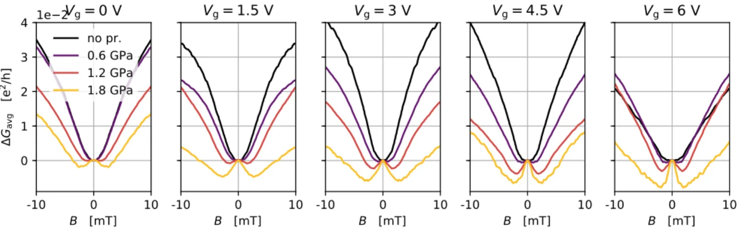
In Figure S2, we present detailed comparison of the magneto-conductance curves at different gate voltages. Each curve is made by an averaging of all the recorded curves within a ±1.5 V range around the value indicated in the panel title. It is visible that the growing tendency of the WAL peak is present at all gate voltages and therefore this is a robust result of the pressure change.
-10 0 10
B [mT]
0 1 2 3 4
G
avg[e
2/h ]
1e 2 V
g= 0 V
no pr.
0.6 GPa 1.2 GPa 1.8 GPa
-10 0 10
B [mT]
V
g= 1.5 V
-10 0 10
B [mT]
V
g= 3 V
-10 0 10
B [mT]
V
g= 4.5 V
-10 0 10
B [mT]
V
g= 6 V
FIG. S2. Comparison of magneto-conductance curves at different gate voltages. Each curve is made by an averaging of all the recorded curves within a ±1.5 V range around the value indicated in the panel title. The colors mark the same pressure on each plot. The WAL peak is more pronounced at all gate voltages as the pressure is increased, which suggests that the increasing pressure has an influence on the enhanced WAL feature independently on other, gate-dependent scattering mechanisms. Conductance correction above 5 mT includes a pronounced contribution of UCF which leads to irregular curve shapes. In addition, gate voltage dependence of the line shape is also clearly visible. The peak amplitude grows with the gate voltage, which is in agreement with Ref. [1] and can be explained with the change of other time scales along with the ones associated to SOC. This tendency is present at every pressure. Due to this dependence on gate voltage, one has to find a balance between reducing the effect of UCF sufficiently and not to average over a gate voltage range where the physical processes differ too much. After investigating the gate voltage measurements and magneto-conductance curves averaged over different gate voltage ranges, we found that the curves of 4 V±1.5 V give a good compromise. This is the setting we used for the fitting.
3 TEMPERATURE DEPENDENCE
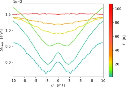
Here, we present in Figure S3 the temperature dependence of the symmetrized magneto-conductance curves at maximum pressure with averaging between 0 V and 2 V gate voltage. It is visible that the WAL peak disappears and the background is negligible above 30 K at low magnetic fields.
-10 -8 -5 -3 0 3 5 8 10
B [mT]
0.0 0.5 1.0 1.5
G
avg[e
2/h ]
1e 2
20 40 60 80 100
T [K ]
FIG. S3. Temperature dependence of the WAL signal at p = 1.8 GPa. The amplitude of the WAL peak decreases with increasing temperature due to the reduction ofτϕ. The curves are shifted by 0.003e2/hfor clarity.
FITTING METHOD
If the scattering times of the SOC (τasy, τsym) are comparable to the intervalley scattering time (τiv), both SOC and chirality influences the magneto-conductivity at the same B field scale, and a unified formula is needed to describe the weak localization behaviour. This can be derived from Ref. [2], as has been done in Ref. [3]:
∆σ(B) =−1 2
e2 πh
F
τB−1 τϕ−1
−F
τB−1 τϕ−1+ 2τasy−1
−2F τB−1 τϕ−1+τasy−1+τsym−1
−F
τB−1 τϕ−1+ 2τiv−1
−2F τB−1 τϕ−1+τiv−1+τia−1
+F
τB−1 τϕ−1+ 2τiv−1+ 2τasy−1
+ 2F τB−1
τϕ−1+τiv−1+τia−1+ 2τasy−1
+ 2F τB−1
τϕ−1+ 2τiv−1+τasy−1+τsym−1
+4F τB−1
τϕ−1+τiv−1+τia−1+τasy−1+τsym−1
,
(1)
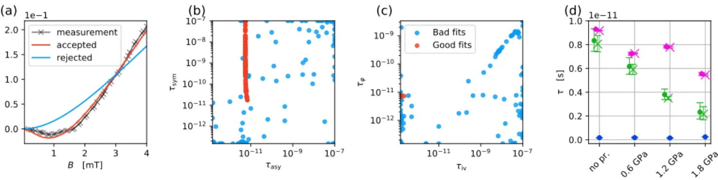
where τia−1 is a scattering rate due to the intravalley scattering due to soft potentials and to the trigonal warping, together. This 5-parameter formula simplifies to the 3-parameter formula used in the main text if τiv−1, τia−1 τϕ−1, τasy−1, τsym−1. Remarkably, this complete formula is invariant under the pairwise interchange of rates (τasy−1, τsym−1) and (τiv−1, τia−1), i.e. chirality and SOC contribute to the magneto-conductivity in the same manner. We note that we present this form of the expression instead of using the commonly used substitution ofτ*−1 =τiv−1+τia−1 to emphasize the symmetry of SOC and scattering parameters. This symmetry makes the interpretation of the fit variables ambiguous unless the value of at least one of the parameters can be determined via an independent measurement. We assume that the momentum relaxation timeτm, extracted from the gate voltage measurements for each pressure, corresponds to the intravalley scattering timeτia, which is shorter than any other time scale. Therefore, during curve fitting, the measured value ofτm is used as the value of the fixed parameterτia leaving only 4 parameters to optimize; and as a lower bound for all other time parameters for both the 3-parameter and the 5-parameter formulas.
Due to the complex shape of the fit formulas, one can expect multiple fit parameter sets that approximate a measured signal reasonably well. To assess the uncertainty associated to the fitting parameters of this origin, we introduce a fitting method called “grid fit” that is described in the following. During the curve fitting of a single magneto-conductivity curve, we do not search for the global best fit, but we look for all the sufficiently good fits in the parameter space. To this end, we create a grid of starting parameters in the 3D parameter space of (τϕ, τasy, τsym) for the 3-parameter formula, or the 4D parameter space (τϕ, τasy, τsym, τiv) of the 5-parameter formula (asτiais fixed), and we start a Levenberg-Marquardt fitting algorithm at each grid point. We accepted the fit if the reduced chi-squared statistic of the fit result was reasonably close to the best value observed in the whole grid. The start points’ grid extends for each time parameter from the actual value ofτmfor each pressure to an upper limit of 1·10−11s, which we consider as a reasonable upper limit forτϕat the measurement temperature and therefore for any other time scale that has a visible influence on the magneto-conductivity curves. Since we looked at parameter values extending over multiple order of magnitude, the distribution of the grid points for each parameter was log-uniform, i.e. the values of lnτi were equidistant fori∈ {ϕ,asy,sym}in the studied range.
All the accepted fits approximate the measurement data equally well for both formulas, with point-to-point dif- ferences of the curves 3 orders of magnitude smaller than the measurement values. In Figure S4b-c, a summary of the fit parameters is shown as an example for the grid fit of the 0.6 GPa curve using the 5-parameter formula. The result of each executed fit is represented by a pair of points on the two panels. The position of the points correspond to the fit values of the parameters marked on the axes, and the red color marks the accepted fits. Fits that were a result of the Levenberg-Marquardt algorithm started from a parameter grid point but got rejected due to their high reduced chi-squared statistic are marked by blue. For the parametersτϕ, τasy, τivthe accepted fit values are concen- trated on a small part of the studied range which suggests reliable fit values. However, similarly to the results using the 3-parameter formula, the value ofτsymcan vary across orders of magnitude without decreasing the fit goodness, meaning that the valley–Zeeman effect does not have any measurable effect on the weak localization behavior in this experiment. Therefore we conclude that the method can not extract reliable value forτsym.
For the other parameters, we consider all the accepted outcomes as physically valid values, since these parameter sets are equivalent in the curve shape. We attribute the geometric mean of the maximum and the minimum of the accepted values as the fit value of the parameter and the upper and lower error boundaries are the minimum and maximum of the accepted outcomes. The results are summarized in Figure S4d. The fit values of τϕ and τasy are
5
1 2 3 4
B [mT]
0.0 0.5 1.0 1.5 2.0 [e2/h]
(a)
1e 1measurement accepted rejected
10 11 10 9 10 7
asy
10 12 10 11 10 10 109 108 107
sym
(b)
10 11 10 9 10 7
iv
10 12 10 11 10 10 109
(c)
Bad fits Good fits
no pr. 0.6 GPa 1.2 GPa 1.8 GPa 0.0
0.2 0.4 0.6 0.8 1.0
[s]
1e 11
(d)
FIG. S4. (a) Example of accepted (red) and rejected (blue) fit results using the 3-parameter formula on the 0.6 GPa curve.
Fit results were accepted based on their reduced chi-squared statistic. (b-c) Summary plots of the fit parameters of the accepted fits to the 0.6 GPa measurement data curve using the complete formula, shown as an example. Every result of the Levenberg-Marquardt method is represented by a pair of dots at the fit value of all the 4 fit parameters. Red dots represent fits that approximate the measurement data reasonably well. Blue dots represent the rejected fit results. (d) Comparison of fit parameters using the formulas. The pink color corresponds toτϕ, the green one toτasy. The cross marker is the fit value using the 3-parameter formula, the dot using the 5-parameter formula. The errorbars represent the minimum and maximum values, the data point is the geometric mean value of the accepted fits. Using the 5-parameter formula, bothτϕandτasyobtain values very close to the results of the 3 parameters formula. The values forτivusing the 5-parameter formula are also plotted with blue. Its small values compared toτϕ andτasy validates the applicability of the 3-parameter formula. The data points are slightly shifted horizontally to avoid overlapping errorbars.
-20 -10 0 10 20
B [mT]
0.5 0.0 0.5 1.0
[e
2/h ] increasing pressure
FIG. S5. Simulated weak anti-localization curves using both the 3-parameter (solid line) and 5-parameter (dotted line) formulas. The curves presented in the main text correspond to the solid lines. The difference of the two curve set is only visible at high magnetic fields, the shape of the central peak is unaffected. Therefore, the two formulas assess the spin orbit times similarly, which supports the parameter fit values in Figure S4d.
very close for both formulas and show the decreasing trend discussed in the main text. The values ofτiv are indeed much smaller than the other time scales, which suggests that the influence of chirality is indeed negligible in our case and the 3-parameter formula is applicable. This is also demonstrated in Figure S5, where 5 pair of simulated curves of the same parameters are plotted using the 3-parameter and the 5-parameter formula. The 3-parameter curves are also shown in Figure 1b of the main text. The τasy and τsym parameters were calculated from the λR and λVZ
parameters, respectively. For the simulation of the pressure,λRwas changed from 300 µeV to 900 µeV in 5 equidistant steps, whereasλVZ was changed from 800 µeV to 2.0 meV in the same manner. The other parameters were fixed for all curves both for the calculation of the magneto-conductivity curves and of the SOC time parameters: τϕ= 1·10−11s, τiv = 1·10−13s, and τia = 1·10−13s. The difference between the 3-parameter and the 5-parameter curves is only visible at higher magnetic fields.
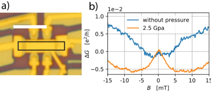
MEASUREMENTS ON ANOTHER DEVICE
Here, we present measurement results on device B. This heterostructure consists of the same layers as device A, and the measured two-terminal segment wasL = 5 µm long andW = 1 µm wide. For this device, a growing WAL peak is also present in the magneto-conductance curves with increasing pressure. However, due to gate instabilities and drifts, a proper comparison of the magneto-conductance curves was not possible.
a) b)
FIG. S6. Measurements of device B. (a) Optical micrograph of the device with the studied segment highlighted by black rectangle. L= 5 µm,W = 1 µm. 4 terminal voltage was measured on the electrodes of the lower side of the picture, but not used during the analysis discussed here. The electrodes on the upper side were left floating. (b) Two terminal magneto-conductance signal, averaged between +2 V and +4 V from the charge neutrality point. This device also exhibits an increasing WAL peak at higher pressures, but a proper comparison of the pressures was not possible due to gate instabilities.
∗ peter.makk@mail.bme.hu
† csonka@mono.eik.bme.hu
[1] F. V. Tikhonenko, D. W. Horsell, R. V. Gorbachev, and A. K. Savchenko, Weak Localization in Graphene FlakesPhys.
Rev. Lett., vol. 100, p. 056802, Feb. 2008.
[2] E. McCann and V. I. Fal’ko, z → −z Symmetry of Spin-Orbit Coupling and Weak Localization in GraphenePhys. Rev.
Lett., vol. 108, p. 166606, Apr. 2012.
[3] S. Zihlmann, A. W. Cummings, J. H. Garcia, M. Kedves, K. Watanabe, T. Taniguchi, C. Schönenberger, and P. Makk, Large spin relaxation anisotropy and valley-Zeeman spin-orbit coupling in WSe2/graphene/h-BN heterostructures Phys.
Rev. B, vol. 97, p. 075434, Feb. 2018.