sciences
Article
Refractive Index Variation of Magnetron-Sputtered a-Si 1 − x Ge x by “One-Sample Concept” Combinatory
Tivadar Lohner, Benjamin Kalas, Peter Petrik *, Zsolt Zolnai, Miklós Serényi and György Sáfrán Institute for Technical Physics and Materials Science, Centre for Energy Research, Hungarian Academy of Sciences, Konkoly-Thege Rd. 29-33, 1121 Budapest, Hungary; lohner.tivadar@energia.mta.hu (T.L.);
kalas.benjamin@energia.mta.hu (B.K.); zsolt.zolnai@energia.mta.hu (Z.Z.);
serenyi.miklos@energia.mta.hu (M.S.); safran.gyorgy@energia.mta.hu (G.S.)
* Correspondence: petrik.peter@energia.mta.hu; Tel.: +36-1-3922502
Received: 12 April 2018; Accepted: 10 May 2018; Published: 21 May 2018
Abstract:Gradient a-Si1−xGexlayers have been deposited by ”one-sample concept” combinatorial direct current (DC) magnetron sputtering onto one-inch-long Si slabs. Characterizations by electron microscopy, ion beam analysis and ellipsometry show that the layers are amorphous with a uniform thickness, small roughness and compositions fromx =0 tox=1 changing linearly with the lateral position. By focused-beam mapping ellipsometry, we show that the optical constants also vary linearly with the lateral position, implying that the optical constants are linear functions of the composition. Both the refractive index and the extinction coefficient can be varied in a broad range for a large spectral region. The precise control and the knowledge of layer properties as a function of composition is of primary importance in many applications from solar cells to sensors.
Keywords:SiGe; spectroscopic ellipsometry; optical properties
1. Introduction
SiGe thin film research is largely motivated by diverse applications in various semiconductor devices [1,2], such as solar cells, thin film transistors [3], Schottky diodes [4], temperature sensors [5], detectors and bolometers [6,7]. However, the effect of the full-scale composition on the properties of thin SiGe films has not been investigated thoroughly; in most of the reports, high film deposition rates have been chosen as a rule instead. The majority of these publications deal with a relatively low Ge concentration [8] and only these films have provided opto-electronic properties suitable for application in device structures. Beyond the special applications, the structure and electrical properties of SiGe alloys have been investigated [9], also for a-Si1−xGexfilms over the entire range of 0≤x≤1 [10].
The actuality of our work is given by the fact that mid-infrared (IR) photonic circuits (mid-IR PCs) have recently gained significance due to the huge number of applications projected over the 2–20µm wavelength range [6,11]. The Si-based technologies have shown a great potential for the implementation of new mid-IR PCs, following a real trend motivated by the large supply of devices already demonstrated at telecom wavelengths [12]. The implementations of SiGe-on-Si is particularly interesting since it allows the fine control of material properties such as the bandgap or the refractive index by balancing the Ge concentration in the alloy, while extending the operation range up to at least 8µm (wavelength of Si absorption onset)—with the possibility of further extending it up to 14µm (Ge transparency cutoff wavelength) for devices with low Si concentration [12,13]. Moreover, Ge presents higher nonlinear properties than Si, hence, preparing Ge-rich structures is a convenient choice to develop nonlinear optical devices in the mid-IR spectral range [14].
Besides chemical vapour deposition (CVD), numerous preparation methods have been used to elaborate this alloy to make a competitive material, however, physical vapor deposition including direct
Appl. Sci.2018,8, 826; doi:10.3390/app8050826 www.mdpi.com/journal/applsci
current (DC) magnetron sputtering method is not extensively used. Two parameters are of primary importance: the low temperature and the high rate of deposition. This technique has the advantages of simplicity, possibility of separating material components, and of relatively high deposition rates.
Materials libraries are deposited mostly by space resolved combinatory using DC magnetron sputtering from two to four targets arranged in a static set-up. The targets are arranged at certain distances from each other above a large substrate or a number of distinct substrates covering the exposed area. As a result of the static arrangements, composition spread alloy films are obtained in which the gradient is not constant and the concentration range is limited; usually, does not cover 0–100%
of the components [15–17]. In this study, we present the preparation of non-hydrogenated gradient SiGe films by DC magnetron sputtering over a surface length of 2 cm. This is a second stage in the development of a combinatorial method [18,19] utilizing the “one sample concept” demonstrated for transmission electron microscopy (TEM) characterizations in smaller samples like TEM grids [20].
The thin film samples have been deposited with different, gradually varying compositions in the whole range and at preparation conditions identical for Si and Ge.
Silicon-based SiGe thin films have been demonstrated for microelectronics, the electronic properties of which are well known. The optical properties of crystalline alloys have also been determined for certain compositions [21,22]. Our objective is to establish the relation between the refractive index and the composition of the layers deposited by the DC magnetron technique. In this article, we show that not only the strictly controlled preparation of a-Si1−xGex films is possible over the entire range of 0 ≤ x ≤ 1 using magnetron sputtering over a length of 2 cm, but the composition, and even more importantly the refractive index (n) and extinction coefficient (k) all show a linear dependence on the position in most of the wavelength range. Using optical measurements by ellipsometry, we demonstrate that our combinatorial setup is suitable for a comprehensive optical characterization of a-Si1−xGex films with accurate spatial and compositional control at a high resolution.
2. ’One-Sample’ Combinatory
The combinatorial a-Si1−xGexsamples with gradient composition ranging in 0 ≤ x ≤ 1 were deposited onto 25×10 mm2size Si slabs by DC magnetron sputtering. We followed the “one sample concept” combinatory in order to cover the entire composition range of a binary film within a single specimen. This is implemented by means of a scaled-up device originally constructed for the preparation of 3-mm diameter micro-combinatorial TEM samples [20]. The present arrangement (Figure1) moves a shutter with a 2×10 mm2slot in fine steps above the substrate while the power of the two magnetron sources is regulated in sync with the position of the slot.
Figure 1.Set-up used for the combinatorial deposition of the a-Si1−xGexlayer.
Using the above method, a combinatorial sample is deposited in form of a 10 mm wide and 25 mm long layer track including a gradient section of 20 mm in length. The gradient part is enclosed in between 2.5 mm long sections of exclusively Si and Ge. The scheme in Figure1depicts the experimental arrangement and the construction of the combinatorial specimen.
A Si-Ge combinatorial sample was deposited as follows: the vacuum system was evacuated to a base pressure of 5×10⁻⁶Pa. The substrate was mounted in the combinatorial device and it was load-locked into the chamber. Ar sputtering gas of partial pressure of 2.5×10⁻¹Pa was introduced.
The Si and Ge targets were cleaned, behind closed shutters, for five minutes applying 340 W and 100 W magnetron power, respectively. These values were selected by preliminary measurements as maximum (100%) of the regulated power of the individual sources, that provided, equally, 0.45 nm/s deposition rates. Subsequently, the slot’s movement of the combinatorial device was started, the shutter of the Si source was opened and Si was deposited at 100% power through the moving slot onto the substrate.
This provided the Si section of the combinatorial track. In due time, the power of the Ge source was set to zero and its shutter was opened. It was followed by the gradual increase of the power of the Ge source, simultaneously, with the decrease of the power of the Si source, so the binary, gradient section of the combinatorial sample was deposited. As the power of the Si source arrived to zero and, simultaneously, that of the Ge arrived to its maximum, the Si source was switched off and, finally, the Ge section of the sample was deposited at 100% power of the Ge source.
3. Distribution of Si and Ge Atomic Fractions
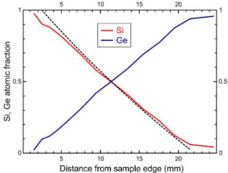
The atomic fractions of Si and Ge were measured by Rutherford backscattering spectrometry (RBS), as shown in Figure2. The RBS analysis was performed in a scattering chamber with a two-axis goniometer connected to the custom-made 5-MV EG-2R Van de Graaff accelerator of the Wigner RMI Institute of the Hungarian Academy of Sciences. The 2-MeV4He+analyzing ion beam was collimated with two sets of four-sector slits to the spot size of 0.5 mm×0.5 mm, while the beam divergence was kept below 0.06◦. The beam current was measured by a transmission Faraday cup [23]. Backscattered He+ions were detected using an ORTEC surface barrier detector (ORTEC, Illinois, USA). The energy resolution of the detection system was 20 keV. Spectra were recorded in Cornell geometry at scattering angle ofΘ=165◦for two different sample tilt angles of 7◦and 60◦. For quantitative compositional analysis, both axial and planar channeling of the He+projectiles in the single-crystalline Si substrate were avoided. The measured data were evaluated with the spectrum simulation code named RBX [24].
Figure 2.Atomic fraction as a function of position along the center line of the combinatorial sample measured by Rutherford backscattering spectrometry. The black dotted line shows the distribution of the atomic fraction based on the calibration using energy dispersive spectrometry (EDS) in a scanning electron microscope.
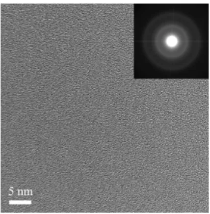
The crystalline quality of single crystalline samples can be qualified by RBS/channeling experiments if the sample is oriented along a major crystalline axis and the yield of the oriented spectrum is compared to the yield of the random, i.e., not oriented spectrum. In our case, oriented (channeling) RBS spectra were not measured, only random spectra were recorded. In the evaluation, we supposed random orientation of the SiGe layer. In this case, a quantitative analysis for the Si/Ge atomic fraction can be performed. On the other hand, selected area electron diffraction pattern represents an amorphous structure (see Figure3).
Figure 3. High resolution TEM image of a 10 nm thick self supporting combinatorial SiGe sample taken for the composition ofx=0.5.
The RBS spectra have been recorded from edge to edge in the center line of the sample. Figure2 reveals that the atomic fraction shows an exactly linear dependence on the position. The distribution is in a good agreement with the calibration based on electron microscopy measurement on a test sample as shown by the black dotted line in the figure.
4. Distribution of the Optical Properties
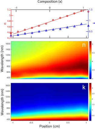
The 25 mm×10 mm combinatorial sample was scanned by a M-2000DI rotating compensator spectroscopic ellipsometer (Woollam Co. Inc., Lincoln, NE, USA). A focused spot has been moved parallel to the long edge along the center line of the wafer. The plane of incidence was parallel to the short edge. The angle of incidence was varied between 60◦and 70◦, and the corresponding size of the focused spot was 0.3 mm wide and 0.6–0.9 mm long. The measurement time was a few seconds for one spot and one angle of incidence. That provided high-resolution and high-accuracy of the data library with a reasonable acquisition time of the entire map (Figure4).
In order to determine the parameters of the deposited a-Si1−xGexfilms, an optical model was constructed to calculate the ellipsometric angles from the model, and to fit the parameters of the model to obtain a good match between the measured and fitted ellipsometry spectra. Since the a-Si1−xGex
film was deposited on a silicon wafer, the model uses a Si substrate assuming a vertically uniform structure, in which only a surface nanoroughness was taken into account by the usual model of mixing 50% layer material with 50% void. The dispersion of the layer was modeled using the Tauc–Lorentz (TL) approach [25]. In this parameterization, the dielectric function is described as a combination of a Lorentz oscillator with the three usual parameters (the broadening, the amplitude and the peak energy position) and an additional Tauc gap parameter. This approach allows that the total number of fitted parameters is kept at a reasonable value (thicknesses of the roughness layer and the film, and the TL parameters. The spectra measured at each position (each composition) have been fitted independently, by changing the above parameters to find the best match between the measured and calculated ellipsometry spectra. The spectra have been recorded at three angles of incidence providing six measured values at each wavelength, and a total of about 2000 measured values for each scanned position. Consequently, the fit was robust, avoiding local minima in the process, resulting in a smooth
map of the optical spectra, as shown by Figure4. Note the smooth changes of the spectra in Figure4in spite of the independent fit procedures at each position, which show the reliability of the fit procedure.
Figure 4.Spectra of the refractive index (n, color map on the middle graph) and the extinction coefficient (k, color map of the bottom graph) as a function of position along the center line of the wafer, calculated using the Tauc–Lorentz (TL) parameterization, as described in the text. Thenandkspectra fitted by the TL model individually can be identified along the vertical axis of the bottom and middle maps, the values of which are color coded at the right hand side of the graphs. The composition of a-Si1−xGex
changes fromx=0 tox=1 over the lateral positions from−1 to 1, as shown in the horizontal axis at the top. The zero position corresponds to the composition ofx=0.5. The top graph showsnandkat the wavelength of 849.7 nm.
The measuredΨand∆spectra fitted by the TL parameterization provide us not only with the thickness of the layer (≈100 nm) and the surface roughness (less than 3 nm) but also withnandk spectra at each spatial position of the sample. The maps in Figure4show those spectra as a function of the position along the center line of the wafer, with the zero position corresponding to the composition ofx=0.5. To check the crystallinity of the layer, High Resolution Transmission Electron Microscope (HRTEM) and selected area electron diffraction (SAED) investigations were carried out by a 300-kV JEOL 3010 HRTEM (Japan Electron Optics Laboratory, Tokyo, Japan) with 0.17 nm point resolution.
Both the granular image contrast and the diffuse rings of the inserted selected area electron diffraction pattern represent an amorphous structure (Figure3).
The most important feature of the optical properties is that bothnandkshow a linear dependence on the position in the whole measured photon energy range, as shown by the color stripes with straight edges corresponding to large changes of the optical properties as a function of the photon energy. This is remarkable, because together with the RBS results of Figure2that indicates a linear dependence of the composition on the position (also shown in Ref. [20]), the linear dependence ofnandkon the position proves that they also linearly depend on the composition (nSi1−xGex(x) = (1−x)×nSi+x×nGeand kSi1−xGex(x) = (1−x)×kSi+x×kGe, wherenSi = 4.33,nGe = 5.33,kSi = 0.46,kGe = 1.10 for the wavelength of 849.7 nm). Bothnandkspan a wide range depending on the composition, indicating
that these properties can well be controlled by properly adjustingxin the a-Si1−xGexcomposition.
It is also important to emphasize that this behavior holds for a broad range of wavelengths. Note that the refractive index can also be modified by hydrogenation, which will be the target of our next study.
In this work, we deal with non-hydrogenated amorphous Si and Ge (see also Ref. [26]).
5. Conclusions
It was shown that the "one-sample concept" combinatorial DC magnetron sputtering developed for transmission electron microscopy characterizations [20] can be up-scaled to a size of one inch, suitable for ellipsometry, with a linear spatial variation of the Si-Ge composition. The real and imaginary parts of the refractive index also show a linear dependence on both the lateral position and the composition in the investigated wavelength range of 350–1650 nm. Using the proposed concept of a:Si1−xGexDC magnetron combinatory, the refractive index and the extinction coefficient can be varied, on purpose, in a broad range at each wavelength.
Author Contributions:G.S. and M.S. prepared the samples. T.L., B.K. and Z.Z. made the measurements and the evaluations. P.P. and M.S. wrote the manuscript.
Acknowledgments: Support from the National Development Agency grant of OTKA K115852, M-ERA.NET WaterSafe, NVKP 16-1-2016-0014 and the Economic Development and Innovation Operative Programme GINOP 2.1.7-15 is greatly acknowledged.
Conflicts of Interest:The authors declare no conflict of interest. The founding sponsors had no role in the design of the study; in the collection, analyses, or interpretation of data; in the writing of the manuscript, and in the decision to publish the results.
References
1. Ferrieu, F. Refined model for spectroscopic ellipsometry analysis of SixGe1−x/Si strained heterostructures.
Appl. Phys. Lett.2000,76, 2023–2025.
2. Hoffmann, L.; Bech Nielsen, B.; Nylandsted Larsen, A.; Leary, P.; Jones, R.; Briddon, P.; Öberg, S.
Substitutional carbon in Si1−xGex. Phys. Rev. B 1999,60, 13573–13581. [CrossRef]
3. Engvall, J.; Nagesh, V.; Grimmeiss, H.; Schreiber, H.U.; Kasper, E. Electrical characterization of SiGe heterostructure bipolar transistors. Thin Solid Films1992,222, 154–156. [CrossRef]
4. Pfeiffer, U.; Mishra, C.; Rassel, R.; Pinkett, S.; Reynolds, S. Schottky barrier diode circuits in silicon for future millimeter-wave and terahertz applications.IEEE Trans. Microw. Theory Tech.2008,56, 364–371. [CrossRef]
5. Rogalski, A. Recent progress in infrared detector technologies. Infrared Phys. Technol. 2011,54, 136–154.
[CrossRef]
6. Sinobad, M.; Monat, C.; Luther-davies, B.; Ma, P.; Madden, S.; Moss, D.J.; Mitchell, A.; Allioux, D.;
Orobtchouk, R.; Boutami, S.; et al. Mid-infrared octave spanning supercontinuum generation to 85µm in silicon-germanium waveguides. Optica2018,5, 360. [CrossRef]
7. Rogalski, A. Heterostructure infrared photovoltaic detectors. Infrared Phys. Technol. 2000,41, 213–238.
[CrossRef]
8. Pickering, C.; Carline, R. Dielectric function spectra of strained and relaxed Si1−xGexalloys (x= 0–0.25).
J. Appl. Phys.1994,75, 4642–4647. [CrossRef]
9. Kosarev, A.; Torres, A.; Hernandez, Y.; Ambrosio, R.; Zuniga, C.; Felter, T.; Asomoza, R.; Kudriavtsev, Y.;
Silva-Gonzalez, R.; Gomez-Barojas, E.; et al. Silicon-germanium films deposited by low-frequency plasma-enhanced chemical vapor deposition: Effect of H2and Ar dilution.J. Mater. Res.2006,21, 88–104.
[CrossRef]
10. Liu, Y.; Dalal, V.L. Properties of amorphous silicon-germanium films and devices deposited at higher growth rates. Mater. Res. Soc. Symp.2002,715, 515–520. [CrossRef]
11. Soref, R. Mid-infrared photonics in silicon and germanium. Nat. Photonics2010,4, 495–497. [CrossRef]
12. Brun, M.; Labeye, P.; Grand, G.; Hartmann, J.M.; Boulila, F.; Carras, M.; Nicoletti, S. Low loss SiGe graded index waveguides for mid-IR applications.Opt. Express2014,22, 508–518. [CrossRef] [PubMed]
13. Ramirez, J.M.; Vakarin, V.; Frigerio, J.; Chaisakul, P.; Chrastina, D.; Le Roux, X.; Ballabio, A.; Vivien, L.;
Isella, G.; Marris-Morini, D. Ge-rich graded-index Si_1-xGex waveguides with broadband tight mode confinement and flat anomalous dispersion for nonlinear mid-infrared photonics. Opt. Express 2017, 25, 6561–6567. [CrossRef] [PubMed]
14. Carletti, L.; Sinobad, M.; Ma, P.; Yu, Y.; Allioux, D.; Orobtchouk, R.; Brun, M.; Ortiz, S.; Labeye, P.;
Hartmann, J.M.; et al. Nonlinear optical response of low loss silicon germanium waveguides in the mid-infrared.Opt. Express2015,23, 8261–8271. [CrossRef] [PubMed]
15. Grochla, D.; Siegel, A.; Hamann, S.; Buenconsejo, P.J.; Kieschnick, M.; Brunken, H.; König, D.; Ludwig, A.
Time- and space-resolved high-throughput characterization of stresses during sputtering and thermal processing of Al-Cr-N thin films.J. Phys. D2013,46, 084011. [CrossRef]
16. Kadletz, P.; Motemani, Y.; Iannotta, J.; Salomon, S.; Khare, C.; Grossmann, L.; Maier, H.; Ludwig, A.;
Schmahl, W. Crystallographic Structure Analysis of a Ti-Ta Thin Film Materials Library Fabricated by Combinatorial Magnetron Sputtering. ACS Comb. Sci.2018,20, 137–150. [CrossRef] [PubMed]
17. Mao, F.; Nyberg, T.; Thersleff, T.; Andersson, A.; Jansson, U. Combinatorial magnetron sputtering of AgFeO2 thin films with the delafossite structure. Mater. Des.2016,91, 132–142. [CrossRef]
18. Kovács, A.; Barna, P.B.; Lábár, J.L. The nucleation and growth of intermetallic Al-Pt phases in co-deposited thin films. Thin Solid Films2003,433, 78–81. [CrossRef]
19. Hung, L.S.; Nastase, M.; Gyulai, J.; Mayer, J.W. Ioninduced amorphous and crystalline phase formation in Al/Ni, Al/Pd, and Al/Pt thin films.Appl. Phys. Lett.1983,42, 672–674. [CrossRef]
20. Sáfrán, G. ‘One-sample concept’ micro-combinatory for high throughput TEM of binary films. Ultramicroscopy 2018,187, 50–55. [CrossRef] [PubMed]
21. Humlíˇcek, J.; Garriga, M.; Alonso, M.I.; Cardona, M. Optical spectra of SixGe1−xalloys. J. Appl. Phys.1989, 65, 2827–2832. [CrossRef]
22. Schmidt, J.; Eilert, M.; Peters, S.; Wietler, T.F. Characterization of thin SiGe layers on Si (001) by spectroscopic ellipsometry for Ge fractions from 0 to 100%. Appl. Surf. Sci.2017,421, 2827–2832. [CrossRef]
23. Pászti, F.; Manuaba, A.; Hajdu, C.; Melo, A.A.; Silva, M.F.D. Current measurement on MeV energy ion beams.Nucl. Instrum. Methods1990,47, 187–192. [CrossRef]
24. Kótai, E. Computer methods for analysis and simulation of RBS and ERDA spectra. Nucl. Instrum. Methods B 1994,85, 588–596. [CrossRef]
25. Jellison, G.E.; Modine, F. Parameterization of the optical functions of amorphous materials in the interband region. Appl. Phys. Lett.1996,69, 371–373. [CrossRef]
26. Collins, R.W.; Windischmann, H.; Cavese, J.M.; Gonzalez-Hernandez, J. Optical properties of dense thin-film Si and Ge prepared by ion-beam sputtering.J. Appl. Phys.1985,58, 954–957. [CrossRef]
c
2018 by the authors. Licensee MDPI, Basel, Switzerland. This article is an open access article distributed under the terms and conditions of the Creative Commons Attribution (CC BY) license (http://creativecommons.org/licenses/by/4.0/).