Correction of the Concentration Profile of the Epitaxially Grown GaAs Thin Film Layers, Measured by Electrolytic Capacitance-Voltage
Method
Antal Ürmös, Ákos Nemcsics
Óbuda University, Institute of Microelectronics and Technology, Tavaszmező utca 17, H-1084, Budapest, Hungary E-mails: urmos.antal @ phd.uni-obuda.hu and nemcsics.akos@kvk.uni-obuda.hu
Abstract— In this work we are dealing with the solution of a concentration profile measurement problem in the epitaxially grown III/V type compound semiconductor layers. The III/V based materials have specific electronic and optical properties, so they have large significance in the semiconductor device production. At these materials, the epitaxial growth is the fundamental technological step.
During this epitaxial process is possible to change the doping concentration in the grown layer. In most cases, the electrolytic capacitance-voltage (ECV) technique serves for the measurement of this concentration profile. This method combines the conventional capacitance-voltage (CV) measurement with the anodic oxidation, to avoid the electrical break-down at the junction. The disadvantage of this method is that the contact surface increases during the measurement, because of the dissolution of the material.
This surface growth - in certain layer structure - causes error in the measurement. In present work, we give a computational solution for this problem by our software, which we have developed in Matlab™. This algorithm calculates and summarizes the wall capacitance and subtract from the measured data, in each step. We demonstrate the operation of the program on different sample data series.
I. INTRODUCTION
The new applications of semiconductors (for instance microwave and optical communications) directed the researchers attention to the family of III/V compound semiconductors (e.g. GaAs, InP etc.). Many favorable properties (e.g.: direct band transition, higher charge carrier mobility) allows us to make such electronic devices, which we cannot prepare from silicon or we can produce only with lower parameters.
In the technology of III/V-based compound semiconductors, the epitaxial growth is one of the most important step. Usually, in the silicon-based device technology, the differently doped layers are made by process of diffusion. This method is not applicable in case of compound semiconductors, because of thermal decomposition. During the epitaxial growth is possible to change the doping concentration of the growing layer, so a proposed concentration profile can be created. However not only the dopant, but the components of the semiconductors are also changeable. Hereby, the heterostructures of these materials can be produced by this method as well.
In the different semiconductor technologies, the various qualifying measurements have very important role. These studies give us a chance to verify, for instance how we realized the required dopant distribution layer. For this goal, in most cases we apply the CV measurement. The disadvantage of this method is an electrical break-down of the junction, when the critical field intensity is reached.
This effect can be avoided by ECV measurement, which essence is, that the semiconductor is contacted with an electrolyte, what is operated like a quasi-Schottky diode [1]. The layer removal is achieved by anodic dissolution of the semiconductor. Nevertheless there is another problem, because the wall capacitance of the etched range falsifies the measured results.
In this article we are looking for the solution of this problem using our software, which we have developed in Matlab™. This algorithm calculates and summarizes the wall capacitance in each step and subtract from the measured data. We demonstrate the operation of the program on different sample data series. In this work, we show the simulation results on a dataset, which contains 8000 measured sample data.
II. DESCRIPTIONOFTHEMEASURINGTECHNIQUE Because of the technological feedback, we need to verify the epitaxially grown layer. One of the most important parameter is the concentration profile. By this property, we can satisfy, whether the realization of the required dopant distribution is successful or not.
The most widely used method to measure the dopant distribution is the CV measurement, because the depth distribution of the free charge carriers is dependent from the capacitance, which is strongly related to dopant profile. Unfortunately, the measurement depth is limited, because of the electrical break-down of the junction, when the critical electrical field intensity is reached. At first - in order to try to avoid this phenomenon – the researchers etched the layer after the measurement, and measured the CV characteristics again. The problem of this method, that the measured results are hardly and inaccurately matched to each other and this work is time-consuming.
In 1973, Ambridge and his colleagues suggested another method. The technique is that the semiconductor is contacted with an electrolyte, which operates as a quasi- Schottky diode. This examination method is the ECV measurement. Compared to other methods, there is an CINTI 2012 • 13th IEEE International Symposium on Computational Intelligence and Informatics • 20–22 November, 2012 • Budapest, Hungary
137 978-1-4673-5206-2/12/$31.00 ©2012 IEEE
advantage of this technique, that the m not limited by the maximum break-down Our experiments are realized b Semiconductor Profile Plotter (Fig. 1), by Polaron Ltd [2]. With this equipmen the III/V-based compound semico concentration profile.
Figure 1. Polaron PN 4100 Semicon The process of the measurement is take the semiconductor sample to an el (Fig. 2.a and 2.b) and apply DC bias vo etching/measurement cycle comes.
A Schottky junction is forme semiconductor and the electrolyte (for NaOH:EDTA).
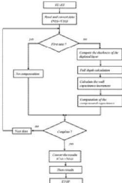
There are two different steps in this first is, that we measure the CV characte and a 30 Hz alternate-current (AC) sig on DC bias. The second is that we During the examination, these two s sequentially. The illumination initia etching, which is caused by the photocu is generated by holes and it is proportio of holes. It is worth to note, that the g photocurrent is realized via valence b carrier concentration at the inner e junction can be computed from CV pro flow chart of the measurement proces problem occurs, that the capacitance of is falsifies the measured data.
III. DISCUSSION The diameter of the contact surfac simulation is performed in 0.01 µm ste capacitance (C’) contains the board (C capacitances (Cm) together. The corre discrete steps - is based on the following the zero step, there is no wall capacit steps, first, we compute the width of and the current wall capacitance. So w capacitance increment. These wall cumulate in each step. This is the mantl subtract the mantle capacitance from th capacitance, so we calculate the concentration. The correction is more pr the finer resolution. In the Fig. 4, w corrected capacitance in blue.
maximum depth is n voltage.
by the PN4100 which is produced nt, we can measure onductor doping
nductor Profile Plotter.
the following: we lectrochemical cell oltage. After them, ed between the
instance Tiron or s experiment. The eristics, by a 3 kHz gnal, superimposed etch the material.
steps are repeated alizes the anodic urrent. This current onal to the number greater part of the band. The charge edge of Schottky ofile. In Fig. 3, the
s is shown. But a f etched range wall
ce is 3 mm. The eps. The measured C) and the mantle ection - made in g consideration: in tance. In the other
the depleted layer we receive the wall capacitances are le capacitance. We he actual measured e charge carrier
recisely, in case of we designated the
Figure 2. The photo of concentration measur so
Figure 3. The flow cha (s
f the measurement unit for the rement (a.) and its structure (b, ource: [1]).
art of the measurement process source: [2]).
A. Ürmös and Á. Nemcsics • Correction of the Concentration Profile of the Epitaxially Grown GaAs Thin Film Layers, Measured…
138
Figure 4. The measured (C’), the m corrected (C) capac The essence of the algorithm, that summarize the wall capacitance in each from measured data. In the Fig. 5, the program is shown.
The first step is to read data a capacitance distribution from the concentration distribution (1). The capacitance distribution of the doping distribution of the doping atom, q is t electron, ε0 is the vacuum permittivity (ε the εr is the relative permittivity (εr = 13 a V is the bias voltage, A is the area of t number of the current step:
The first compensated value is the measured value, because in this case th is zero.
In other cases, first we calculate the depleted layer (w(x)) (2). The Cmeasured(x) distribution of the doping atom, ε0
permittivity, εr is the relative permittivit the surface, x is the number of the curren
The next step is we compute the lcomplete(x) (3). The d is the thickness of the is the step size of the simulation), w(x) i
mantle (Cm) and the citance.
we compute and h step, and subtract e flowchart of this and calculate the e doping atom
Cmeasured(x) is the
atom, N(x) is the the charge of one ε0 = 8.9*10-12 F/m), 3 in case of GaAs), the surface, x is the
√ . (1) same as the first he wall capacitance e thickness of the ) is the capacitance
0 is the vacuum ty, A is the area of nt step:
. (2) e complete depth
e etched layer (this is the thickness of
Figure 5. The flow chart the depleted layer (x is the n calculated by (2):
After this, we calculate the w (Cwall(x)) (4). The ε0 is the vac relative permittivity, A is the a number of the current step:
In the next formula, w capacitance, which is the – a capacitance (Cmantle(x)) and the (5):
∑ After this, the mantle capaci from measured capacitance (Cm
The Ccorrected(x) is the result.
Finally, we calculate the c distribution (7). The Ncorrected(x) i of the doping atom, q is the ch the vacuum permittivity, the εr
a V is the bias voltage, A is the number of the current step:
t of the compensation algorithm.
number of the current step)
. (3) wall capacitance increment
cuum permittivity, εr is the area of the surface, x is the
. (4) we summarize the wall above mentioned – mantle
k is the running variable
∑ . (5) tance Cmantle(x) is subtracted
measured(x)) (6):
. (6)
compensated doping atom is the corrected distribution harge of one electron, ε0 is is the relative permittivity, area of the surface, x is the
√ . (7) CINTI 2012 • 13th IEEE International Symposium on Computational Intelligence and Informatics • 20–22 November, 2012 • Budapest, Hungary
139
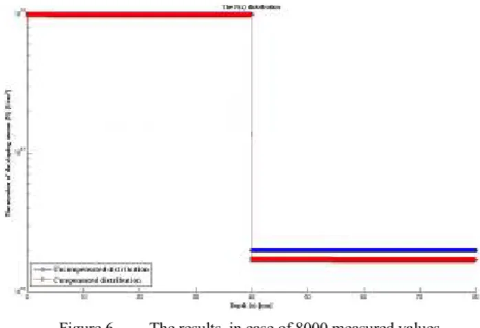
In the Fig. 6, we can follow the operation of the described algorithm, in a sample dataset, which contains 8000 measured value. In the horizontal axis we show the depth (in linear scale) and in the vertical axis we represent the charge carrier concentration (in logarithmic scale).
Figure 6. The results, in case of 8000 measured values.
REFERENCES
[1] Nemcsics Ákos, „Az epitaxiális GaAs rétegszerkezetek minősítése elektrolitos C-V méréssel,” Elektronikai Technológia, Mikro- technika, pp. 78-90, 1993.
[2] Polaron PN4100 Semiconductor Profile Plotter Instruction Manual, 1982.
A. Ürmös and Á. Nemcsics • Correction of the Concentration Profile of the Epitaxially Grown GaAs Thin Film Layers, Measured…
140